Innophase Talaria TWO INP3010 User manual

Talaria TWOTM EVB-A Evaluation Boards
(INP3010 / INP3011 / INP3012 / INP3013)
Extreme Low Power Wireless Platform
IEEE 802.11 b/g/n, BLE5
User Guide for Talaria TWOTM
Evaluation & Development Kit
Version 2.0
Copyright ©InnoPhase, Inc., 2021 All Rights Reserved
InnoPhase, Inc.
6815 Flanders Drive
San Diego, CA 92121
innophaseinc.com

Talaria TWOTM Evaluation & Development Kit
Version 2.0 1 ©InnoPhase, Inc. 2021
Contents
1Figures......................................................................................................................................3
2Tables.......................................................................................................................................3
3Terms & Definitions .................................................................................................................4
4Introduction .............................................................................................................................5
5INP301x Package Contents .....................................................................................................5
6Description of the board..........................................................................................................6
6.1 Block Diagram....................................................................................................................6
6.2 Jumpers on the board........................................................................................................8
6.3 Power Supply and Mode Switch........................................................................................9
6.4 IO Header (J1) ..................................................................................................................10
6.5 Shield Headers (JP1 to JP4)..............................................................................................11
6.6 On Board Sensors ............................................................................................................12
7Functional Description...........................................................................................................13
7.1 Stand-alone mode ...........................................................................................................13
7.1.1 Driver Installation for Windows OS..........................................................................14
7.2 Shield Mode.....................................................................................................................19
7.2.1 EVB-A as Wi-Fi Shield with STM32 Nucleo Board ....................................................19
8Power Measurement .............................................................................................................20
9Using Battery as Power Source..............................................................................................21
10 FCC/ISED Regulatory Notices ..............................................................................................22
10.1 Modification Statement...................................................................................................22
10.2 Interference Statement ...................................................................................................22
10.3 Radio Frequency Radiation Exposure Statement............................................................22
10.4 RF Exposure Statement for Module Integration .............................................................23
10.5 Labeling Requirements for the Host Device....................................................................24
10.5.1 INP1010 ....................................................................................................................25
10.5.2 INP1011 ....................................................................................................................25
10.5.3 INP1012 ....................................................................................................................26
10.5.4 INP1013 ....................................................................................................................26
11 Support................................................................................................................................27


Talaria TWOTM Evaluation & Development Kit
Version 2.0 3 ©InnoPhase, Inc. 2021
1Figures
Figure 1: INP301x EVB-A Board with INP101x module board installed ................................................................ 5
Figure 2: Block diagram of INP301x Evaluation Board.......................................................................................... 6
Figure 3: INP301x EVB-A control and connectivity points .................................................................................... 8
Figure 4: Power supply section ............................................................................................................................. 9
Figure 5: IO Header.............................................................................................................................................. 10
Figure 6: Arduino UNO shield compatible jumpers ............................................................................................ 11
Figure 7: On board sensors ................................................................................................................................. 12
Figure 8: Listing devices in Zadig......................................................................................................................... 14
Figure 9: Updating Talaria TWOTM USB driver to libusbK.................................................................................... 15
Figure 10: Device Manager.................................................................................................................................. 16
Figure 11: Update Devices................................................................................................................................... 17
Figure 12: Select the device driver...................................................................................................................... 18
Figure 13: INP3010 EVB-A as Wi-Fi Shield........................................................................................................... 19
Figure 14: Current measurement setup using Otti Arc....................................................................................... 20
Figure 15: J10 Battery connection....................................................................................................................... 21
Figure 16: Labelling requirement - INP1010 ....................................................................................................... 25
Figure 17: Labelling requirement - INP1011 ....................................................................................................... 25
Figure 18: Labelling requirement - INP1012 ....................................................................................................... 26
Figure 19: Labelling requirement - INP1012 ....................................................................................................... 26
2Tables
Table 1: Jumper Information................................................................................................................................. 8
Table 2: FTDI Layout ............................................................................................................................................ 13

Talaria TWOTM Evaluation & Development Kit
Version 2.0 4 ©InnoPhase, Inc. 2021
3Terms & Definitions
BLE Bluetooth Low Energy
DMM Digital Multimeter
DPDT Double Pole Double Throw
FTDI Future Technology Devices International
GPIO General Purpose Input/Output
IO Input Output
JTAG Joint Test Action Group
LED Light Emitting Diode
MPSEE Multi-Protocol Synchronous Serial Engine
SCL Serial Clock
SDA Serial Data
SPI Serial Peripheral Interface
SPDT Single Pole Double Throw
UART Universal Asynchronous Receiver-Transmitter
USB Universal Serial Bus

Talaria TWOTM Evaluation & Development Kit
Version 2.0 5 ©InnoPhase, Inc. 2021
4Introduction
INP301x Talaria TWOTM evaluation board is designed as an evaluation platform for the INP101x
modules. This user guide provides an overview of the evaluation board explaining its key features and
functions.
5INP301x Package Contents
The package contains:
1. INP3010*, INP3011**, INP3012 or INP3013 board
2. Micro USB cable
3. Antenna (INP3011 and INP3012 boards)
4. Battery box
Figure 1: INP301x EVB-A Board with INP101x module board installed
*INP3010: EVB boards having INP1010 module with PCB antenna
**INP3011: EVB boards having INP1011 module with U.FL antenna connector
Talaria TWOTM Evaluation & Development Kit
Version 2.0 6 ©InnoPhase, Inc. 2021
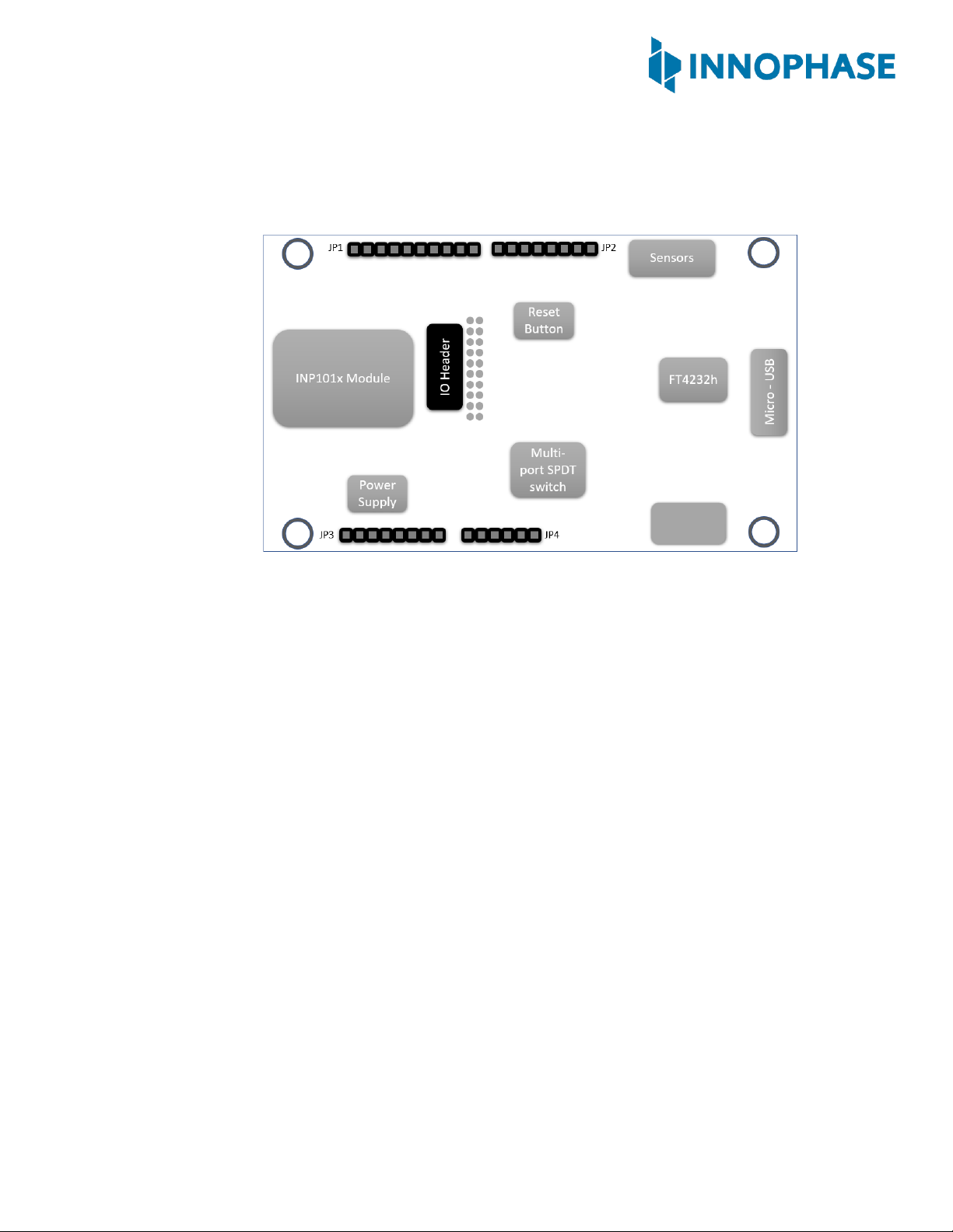
6Description of the board
6.1 Block Diagram
Figure 2: Block diagram of INP301x Evaluation Board
The block diagram of the INP301x Evaluation board is shown in Figure 2. The main component on
the board is the INP101x module. Key features of the evaluation board are:
1. Standalone mode vs. Shield mode: Using the mode switch U3, either standalone mode or
shield mode can be selected.
a. In standalone mode, the INP101x can be accessed via micro-USB cable for
programming and debugging. This mode is recommended for standalone
application development.
b. In shield mode, the INP101x module can be interfaced with any host CPU and can
provide serial to Wi-Fi capabilities.
2. A peripheral IO header (J1) is available using which all the IO’s of the INP101x module can
be accessed.
3. Power supply section: Based on the mode, the power for module is derived from either
USB or shield header. A battery header is available which can be used as power source as
well.
a. J4 at VM_3.3V for USB power
b. J4 at VBAT and battery connect to J10 for Battery power
Switch
(Standalone vs
Shield mode)

Talaria TWOTM Evaluation & Development Kit
Version 2.0 7 ©InnoPhase, Inc. 2021
4. On board sensors are available to develop sensor to cloud applications.
5. Switch:
a. Set U3 switch to V33_ARD for Shield mode
b. Set U3 switch to V_3.3V for Standalone mode

Talaria TWOTM Evaluation & Development Kit
Version 2.0 8 ©InnoPhase, Inc. 2021
6.2 Jumpers on the board
Figure 3: INP301x EVB-A control and connectivity points
Jumper
Mode and Operation
J1
IO header
J2
Used to enable Console logging in shield mode
J3
Connect LED D1 to GPIO14, for debug purposes
J4
Select power from USB or battery connector, also used for current
measurements
J7
Connect SCL to GPIO4
J8
Connect SDA to GPIO3
J9
Select IO voltage for FTDI IOs
J10
Battery terminal
J11
Enable the multi-port SPDT switch
JP1 to JP4
Arduino UNO shield compatible header (3.3V support only)
U3
Switch between Stand-alone mode and Arduino Shield Mode
Table 1: Jumper Information
Talaria TWOTM Evaluation & Development Kit
Version 2.0 9 ©InnoPhase, Inc. 2021
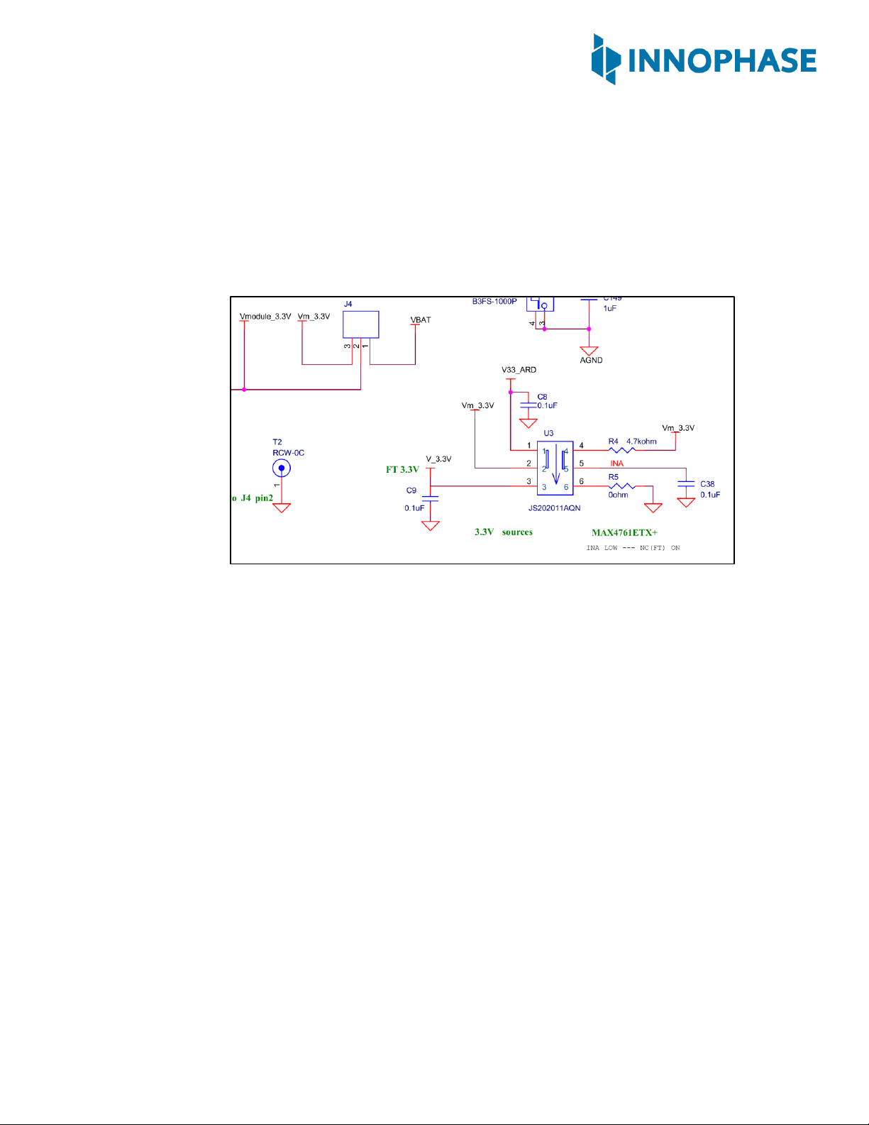
6.3 Power Supply and Mode Switch
The INP301x board is designed to supply power to the INP101x module in following ways:
1. In standalone mode, power is drawn from USB connector
2. In shield mode, power is drawn from shield connector
3. A battery header is also available to provide power to the module
Figure 4: Power supply section
The power supply section is shown in the Figure 4. The INP101x module requires 3.3V supply. The
DPDT switch (U3) selects between USB and Arduino header supply using the common net
Vm_3.3V. The jumper J4 is used to select between battery supply and Vm_3.3V. The same jumper
can be used for measuring current consumption of the module.

Talaria TWOTM Evaluation & Development Kit
Version 2.0 10 ©InnoPhase, Inc. 2021
6.4 IO Header (J1)
The J1 header brings out all the IOs from INP101x module. These IOs can be used for debug, and/or
any external interfacing needs. The pinout of this header is shown in Figure 5. To work with on
board sensor, pins 1 & 2 needs to be shorted.
Figure 5: IO Header
Talaria TWOTM Evaluation & Development Kit
Version 2.0 11 ©InnoPhase, Inc. 2021
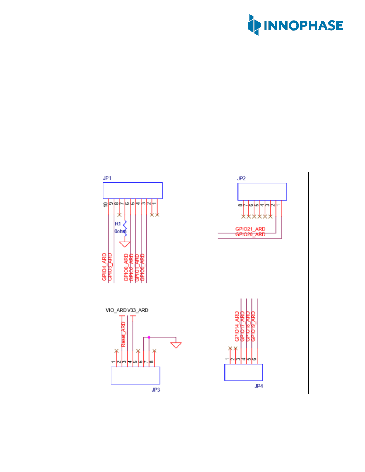
6.5 Shield Headers (JP1 to JP4)
Arduino UNO compatible headers are available in the INP301x board to interface with any
compatible host micro-controller.
The GPIOs assigned to shield headers are carefully chosen to achieve following capability:
1. INP101x’s SPI slave pins available on JP1
2. INP101x’s I2C master pins available on JP1
3. Remaining GPIOs are available on JP2 and JP4
Note that INP301x supports 2.5V IO as the default configuration. The shield header connections
are as shown in JP2 of Figure 6.
Figure 6: Arduino UNO shield compatible jumpers
Talaria TWOTM Evaluation & Development Kit
Version 2.0 12 ©InnoPhase, Inc. 2021
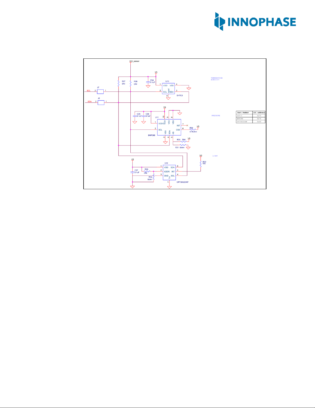
6.6 On Board Sensors
Figure 7: On board sensors
The INP301x board has following sensors available on board for quick prototyping/testing:
1. Temperature/Humidity (Sensirion SHTC3)
2. Pressure (Bosch BMP388)
3. Light (TI OPT3002)
To use the sensors, J7, J8, pins 1 & 2 of J1 should be connected. This enables power connection
to the sensors on board, I2C connection on GPIOs 3 & 4.
Talaria TWOTM Evaluation & Development Kit
Version 2.0 13 ©InnoPhase, Inc. 2021
7Functional Description
Following are the functional modes that can be achieved in the INP301x board:
1. Stand-alone mode (host-less)
2. Shield mode (hosted)
More details about each mode are available in subsequent sections. Switching between the modes is
handled by DPDT switch U3 for power, and multi-port SPDT switch U1 for the GPIOs.
7.1 Stand-alone mode
The stand-alone mode is intended for following use cases:
1. Host-less application development on INP101x modules
2. Programing access to INP101x modules
In stand-alone mode, the U3 switch is pushed towards pin 3, which disconnects power and IO
from shield headers and connects them to FTDI. The FTDI port layout is shown in Table 2.
FTDI Bus
Interface to Talaria TWOTM
A
JTAG
B
RESET
C
UART
D
CONSOLE (UART)
Table 2: FTDI Layout
The A & B bus of FTDI device supports MPSEE protocol, hence JTAG is assigned to A-bus. The
BDBUS7 is connected EN_CHIP of the INP101x module. The C & D bus of FTDI device used as
UARTs, with C-bus connected to peripheral UART of INP101x module and D-bus connected is
CONSOLE port (GPIO17) of INP101x module.
The JTAG on A-bus is used for debugging applications on the INP101x module. The UART on C-bus
is used for programming the INP101x module. The CONSOLE port is a unidirectional UART from
INP101x module that operates at high baud rate of 2457600, used for debug prints.
Talaria TWOTM Evaluation & Development Kit
Version 2.0 14 ©InnoPhase, Inc. 2021
7.1.1 Driver Installation for Windows OS
On Windows OS, libusbK driver needs to be installed to communicate and control the
Talaria TWOTM module via the FTDI device on the evaluation board. The tools/applications
provided by InnoPhase will use this driver. Install/uninstall instructions for this driver is given
subsequent sections.
7.1.1.1 Installation instructions for libusbK driver
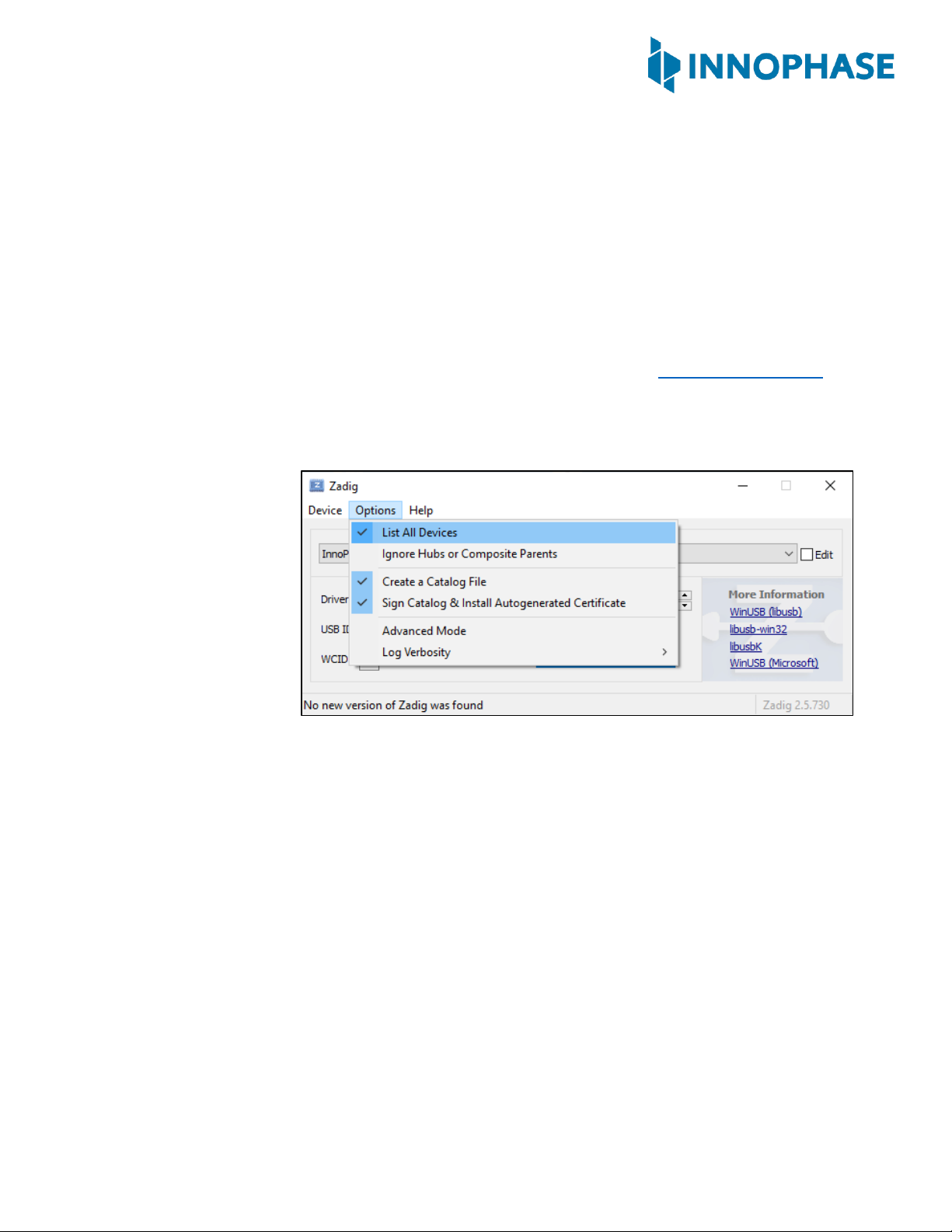
Download the free software Zadig, available here: - https://zadig.akeo.ie/. Connect
your Windows PC or Laptop to the evaluation board using the provided USB cable.
Now, open Zadig and click on Options. Select List All Devices and deselect
Ignore Hubs or Composite Parents as shown in Figure 8.
Figure 8: Listing devices in Zadig
Talaria TWOTM Evaluation & Development Kit
Version 2.0 15 ©InnoPhase, Inc. 2021
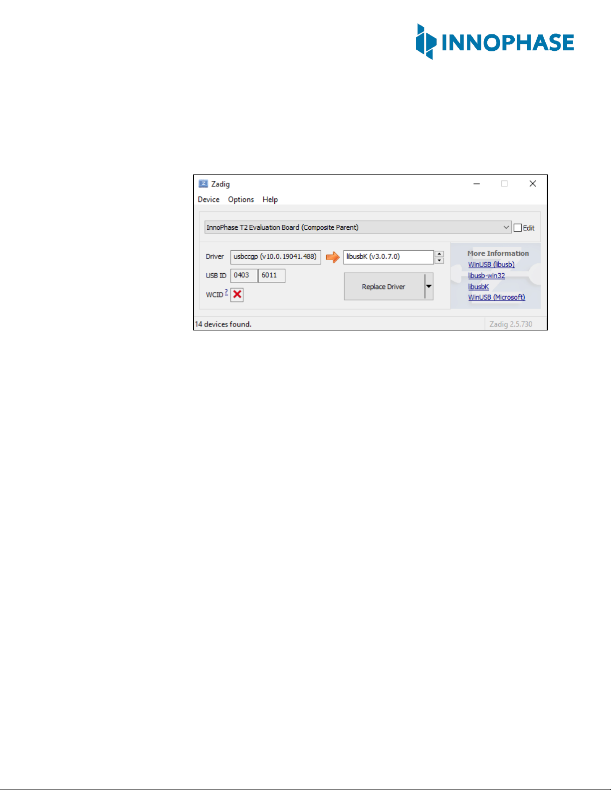
To establish communication with Talaria TWOTM module via the FTDI device on the
InnoPhase Evaluation Board, the Talaria TWOTM USB driver must be libusbK. In
case the current driver is not libusbK, use the drop-down menu to select
libusbK and click on Replace Driver which will update the drivers to
libusbK.
Figure 9: Updating Talaria TWOTM USB driver to libusbK
Talaria TWOTM Evaluation & Development Kit
Version 2.0 16 ©InnoPhase, Inc. 2021
7.1.1.2 Uninstall instructions for libusbK driver
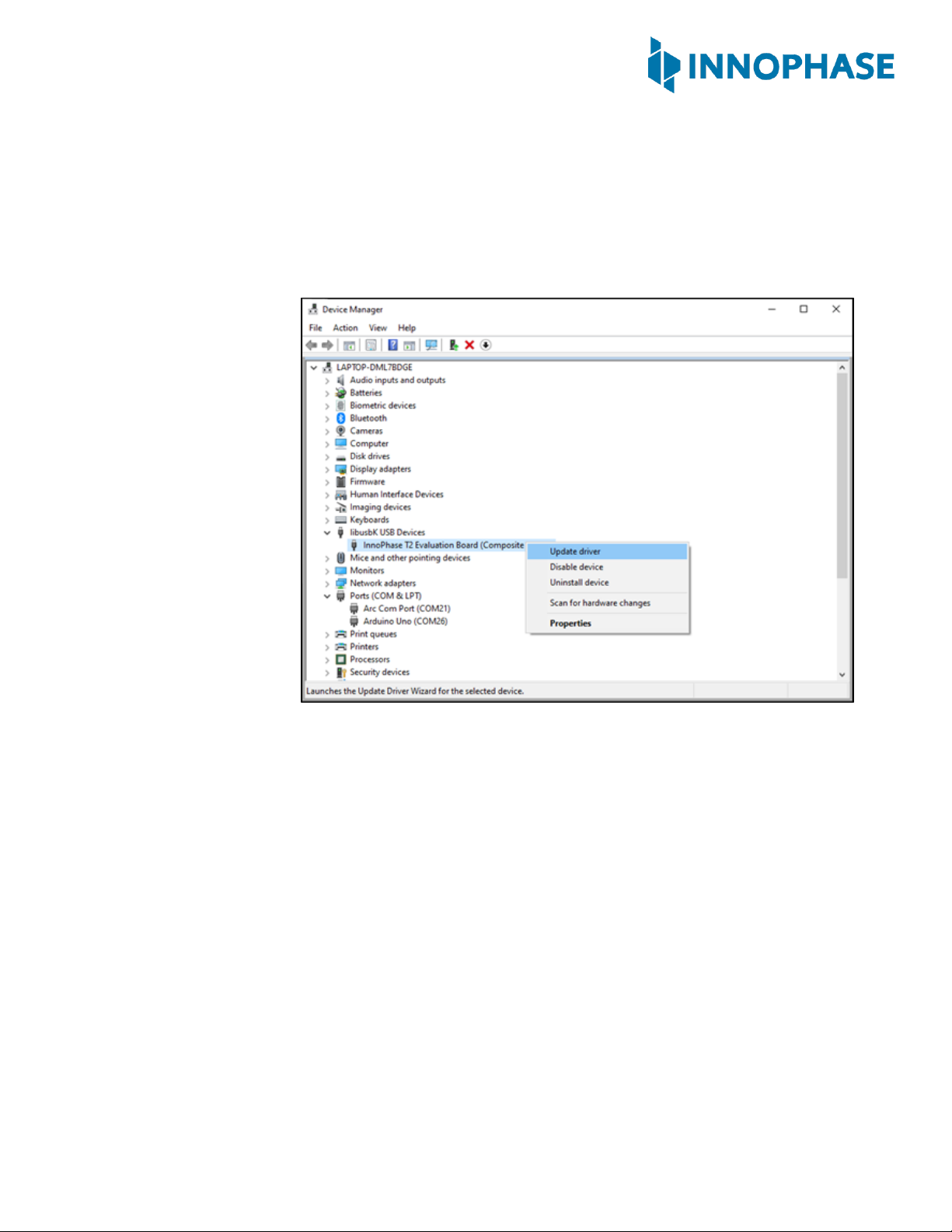
To uninstall libusbK and retrieve COM ports, follow the following steps:
1. Open Device Manager. Expand the libusbK USB Devices and right
click on the InnoPhase T2 Evaluation Board (Composite
Parent). Click on Update Driver as shown in Figure 10.
Figure 10: Device Manager

Talaria TWOTM Evaluation & Development Kit
Version 2.0 17 ©InnoPhase, Inc. 2021
2. On the new window, select Browse computer for drivers, click on Let me
pick from a list of available drivers on my computer
option and click on Next.
Figure 11: Update Devices
Talaria TWOTM Evaluation & Development Kit
Version 2.0 18 ©InnoPhase, Inc. 2021
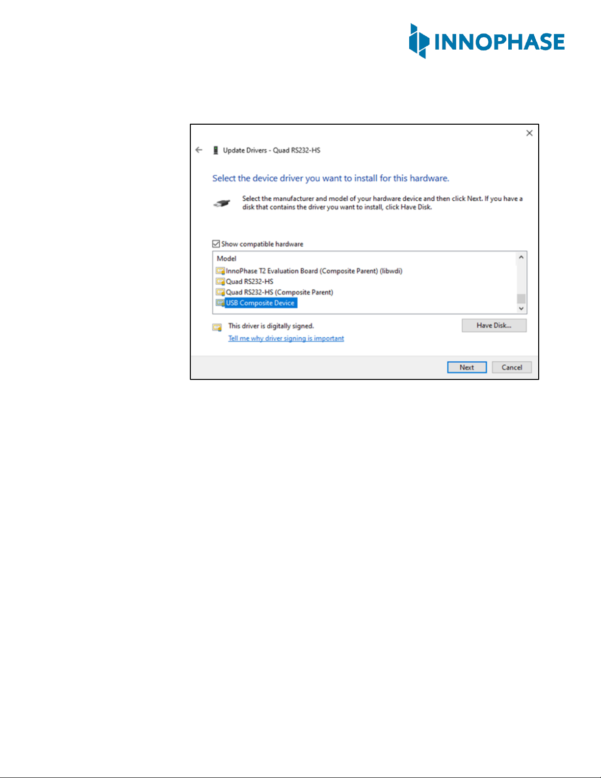
3. Select USB Composite Device and click Next to reinstall the COM
ports.
Figure 12: Select the device driver

Talaria TWOTM Evaluation & Development Kit
Version 2.0 19 ©InnoPhase, Inc. 2021
7.2 Shield Mode
This mode will make the EVB-A board to act as a Wi-Fi/BLE5 shield. To enable this mode, flip the
switch U3 towards V33_ARD. This also pulls up the INA pin of the multi-port SPDT device
MAX4761ETX, which then routes the GPIOs from the INP101x module to the shield headers JP1,
JP2, JP3 and JP4. In the shield mode a suitable firmware (such as Serial to Wi-Fi application
available in the SDK) should be pre-flashed in the INP101x.
7.2.1 EVB-A as Wi-Fi Shield with STM32 Nucleo Board
A comprehensive set of host application packages are available to download via the
InnoPhase website to demonstrate the use of EVB-A as a Wi-Fi/BLE5 shield board.
Figure 13: INP3010 EVB-A as Wi-Fi Shield
Other manuals for Talaria TWO INP3010
1
This manual suits for next models
3
Table of contents
Other Innophase Motherboard manuals

Popular Motherboard manuals by other brands

Intersil
Intersil ISL54302EVAL1Z user manual

ON Semiconductor
ON Semiconductor MT9J003I12STCVH-GEVB user manual

Silicon Laboratories
Silicon Laboratories Thunderboard EFM8UB3 user guide

AZZA-XFX
AZZA-XFX 845S-AV user manual

Supermicro
Supermicro C7B360-CB-M Quick reference guide

Gigabyte
Gigabyte GA-X99-UD7 WIFI user manual


