Innophase Talaria TWO INP3010 User manual

Copyright © | All Rights Reserved | Proprietary Information
InnoPhase IoT, Inc. | 6815 Flanders Drive | San Diego, CA 92121 | https://innophaseiot.com/ | sales@innophaseiot.com
Talaria TWO™ EVB-A Evaluation Boards
(INP3010/INP3011/INP3012/INP3013/INP3014/INP3015)
Ultra-Low Power Multi-Protocol Wireless Platform SoC
IEEE 802.11 b/g/n, BLE 5.0
User Guide for Talaria TWO Evaluation &
Development Kit
Release: 08-26-2022

Talaria TWO Evaluation & Development Kit
Version 5.0 Copyright © | All Rights Reserved | Proprietary 2
Revision History
Version
Date
Comments
1.0
07-04-2020
First version
1.1
09-14-2020
Updated for SDK 2.1.1 release
2.0
05-13-2021
Updated for SDK 2.2 release
Updated block diagram to reflect v1.3 board and jumper settings
2.1
07-09-2021
Updated labels for INP1012/1013
2.2
07-30-2021
Updated Antenna details for INP1010/11/12/13
2.3
08-06-2021
Updated with additional Antenna information for INP10x modules
2.4
08-16-2021
Updated Antenna specifications table for INP10x modules
3.0
10-22-2021
Updated Antenna specifications for INP1014 & INP1015 modules
3.1
10-27-2021
Updated labels for INP1014/15 modules
4.0
12-13-2021
Updated Antenna requirements for INP1015 module
4.1
01-06-2022
Updated labels for INP1014 and 1015 modules
4.2
01-20-2022
Removed Zadig installation requirement for using libusbk drivers
5.0
08-26-2022
Updated with antenna specifications for INP1014 and INP1015

Talaria TWO Evaluation & Development Kit
Version 5.0 Copyright © | All Rights Reserved | Proprietary 3
Contents
Figures..............................................................................................................................................................4
Tables ...............................................................................................................................................................4
Terms & Definitions...........................................................................................................................................5
Introduction........................................................................................................................................................6
INP301x Package Contents...............................................................................................................................6
Description of the Board....................................................................................................................................7
Block Diagram................................................................................................................................................7
Jumpers on the Board....................................................................................................................................8
Power Supply and Mode Switch.....................................................................................................................9
IO Header (J1).............................................................................................................................................10
Shield Headers (JP1 to JP4)........................................................................................................................11
On Board Sensors .......................................................................................................................................12
Functional Description.....................................................................................................................................13
Stand-alone Mode........................................................................................................................................13
Shield Mode.................................................................................................................................................14
EVB-A as Wi-Fi Shield with STM32 Nucleo Board....................................................................................14
Power Measurement .......................................................................................................................................15
Using Battery as Power Source.......................................................................................................................16
Antenna...........................................................................................................................................................17
INP1010.......................................................................................................................................................17
INP1011/INP1012/INP1015 .........................................................................................................................17
INP1013.......................................................................................................................................................18
INP1014.......................................................................................................................................................18
FCC/ISED Regulatory Notices.........................................................................................................................19
Modification Statement.................................................................................................................................19
Interference Statement.................................................................................................................................19
Radio Frequency Radiation Exposure Statement.........................................................................................19
RF Exposure Statement for Module Integration............................................................................................19
Support............................................................................................................................................................20
Disclaimers......................................................................................................................................................21

Talaria TWO Evaluation & Development Kit
Version 5.0 Copyright © | All Rights Reserved | Proprietary 4
Figures
Figure 1: INP301x EVB-A Board with INP101x module board installed .............................................................6
Figure 2: Block diagram of INP301x Evaluation Board ......................................................................................7
Figure 3: INP301x EVB-A control and connectivity points..................................................................................8
Figure 4: Power supply section..........................................................................................................................9
Figure 5: IO Header.........................................................................................................................................10
Figure 6: Arduino UNO shield compatible jumpers ..........................................................................................11
Figure 7: On board sensors.............................................................................................................................12
Figure 8: INP3010 EVB-A as Wi-Fi Shield.......................................................................................................14
Figure 9: Current measurement setup using Otti Arc.......................................................................................15
Figure 10: J10 Battery connection ...................................................................................................................16
Tables
Table 1: Jumper Information..............................................................................................................................8
Table 2: FTDI Layout.......................................................................................................................................13
Table 3: Module ID with Antenna details..........................................................................................................17
Table 4: INP1010 - Antenna specifications......................................................................................................17
Table 5: INP1011/012/015 - Antenna specifications ........................................................................................17
Table 6: INP1013 - Antenna specifications......................................................................................................18
Table 7: INP1014 Antenna specifications........................................................................................................18

Talaria TWO Evaluation & Development Kit
Version 5.0 Copyright © | All Rights Reserved | Proprietary 5
Terms & Definitions
BLE Bluetooth Low Energy
DMM Digital Multimeter
DPDT Double Pole Double Throw
FTDI Future Technology Devices International
GPIO General Purpose Input/Output
IO Input Output
JTAG Joint Test Action Group
LED Light Emitting Diode
MPSEE Multi-Protocol Synchronous Serial Engine
SCL Serial Clock
SDA Serial Data
SPI Serial Peripheral Interface
SPDT Single Pole Double Throw
UART Universal Asynchronous Receiver-Transmitter
USB Universal Serial Bus
Talaria TWO Evaluation & Development Kit
Version 5.0 Copyright © | All Rights Reserved | Proprietary 6
Introduction
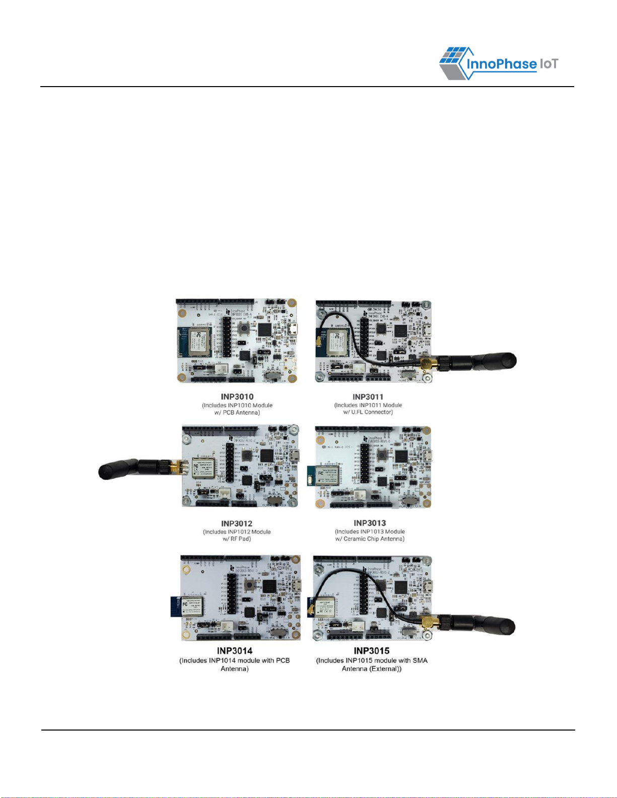
INP301x Talaria TWO evaluation board is designed as an evaluation platform for the INP101x modules. This
user guide provides an overview of the evaluation board explaining its key features and functions.
INP301x Package Contents
The package contains:
1. INP3010*, INP3014*, INP3011**, INP3015**, INP3012 or INP3013 board
2. Micro USB cable
3. Antenna (INP3011 and INP3012 boards)
4. Battery box
Figure 1: INP301x EVB-A Board with INP101x module board installed
Talaria TWO Evaluation & Development Kit
Version 5.0 Copyright © | All Rights Reserved | Proprietary 7
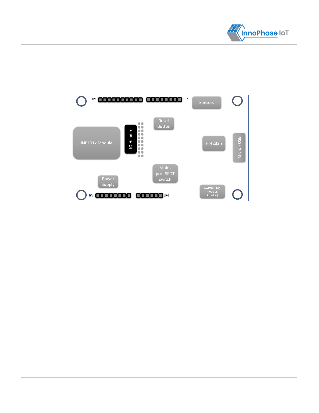
Description of the Board
Block Diagram
Figure 2: Block diagram of INP301x Evaluation Board
The block diagram of the INP301x Evaluation board is shown in Figure 2. The main component on the board is
the INP101x module. Key features of the evaluation board are:
1. Standalone mode vs. Shield mode: Using the mode switch U3, either standalone mode or shield mode
can be selected.
a. In standalone mode, the INP101x can be accessed via micro-USB cable for programming and
debugging. This mode is recommended for standalone application development.
b. In shield mode, the INP101x module can be interfaced with any host CPU and can provide serial
to Wi-Fi capabilities.
2. A peripheral IO header (J1) is available using which all the IO’s of the INP101x module can be accessed.
3. Power supply section: Based on the mode, the power for module is derived from either USB or shield
header. A battery header is available which can be used as power source as well.
a. J4 at VM_3.3V for USB power
b. J4 at VBAT and battery connect to J10 for Battery power
4. On board sensors are available to develop sensor to cloud applications.
5. Switch:
a. Set U3 switch to V33_ARD for Shield mode
b. Set U3 switch to V_3.3V for Standalone mode

Talaria TWO Evaluation & Development Kit
Version 5.0 Copyright © | All Rights Reserved | Proprietary 8
Jumpers on the Board
Figure 3: INP301x EVB-A control and connectivity points
Jumper
Mode and Operation
J1
IO header
J2
Used to enable Console logging in shield mode
J3
Connect LED D1 to GPIO14, for debug purposes
J4
Select power from USB or battery connector, also used for current measurements
J7
Connect SCL to GPIO4
J8
Connect SDA to GPIO3
J9
Select IO voltage for FTDI IOs
J10
Battery terminal
J11
Enable the multi-port SPDT switch
JP1 to JP4
Arduino UNO shield compatible header (3.3V support only)
U3
Switch between Stand-alone mode and Arduino Shield Mode
Table 1: Jumper Information
Talaria TWO Evaluation & Development Kit
Version 5.0 Copyright © | All Rights Reserved | Proprietary 9
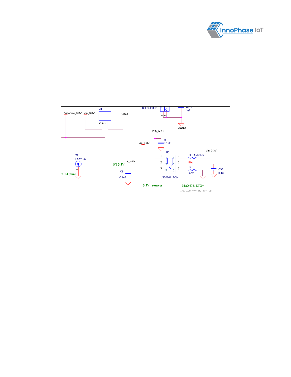
Power Supply and Mode Switch
The INP301x board is designed to supply power to the INP101x module in following ways:
1. In standalone mode, power is drawn from USB connector
2. In shield mode, power is drawn from shield connector
3. A battery header is also available to provide power to the module
Figure 4: Power supply section
The power supply section is shown in Figure 4. The INP101x module requires 3.3V supply. The DPDT switch
(U3) selects between USB and Arduino header supply using the common net Vm_3.3V. The jumper J4 is used
to select between battery supply and Vm_3.3V. The same jumper can be used for measuring current
consumption of the module.
Talaria TWO Evaluation & Development Kit
Version 5.0 Copyright © | All Rights Reserved | Proprietary 10
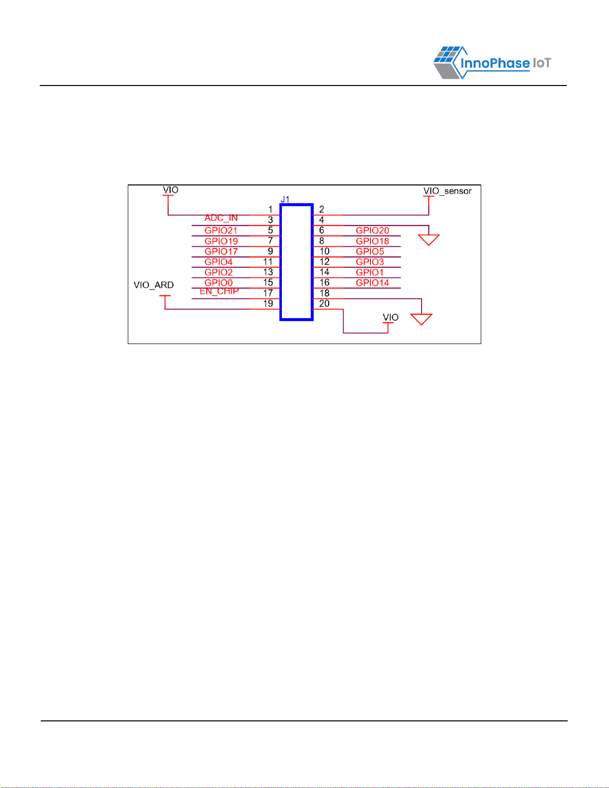
IO Header (J1)
The J1 header bringsout all the IOs from INP101x module. TheseIOs can be used for debug, and/or any external
interfacing needs. Thepinout of this header is shown in Figure 5. To work with on board sensor, pins 1 & 2 needs
to be shorted.
Figure 5: IO Header
Talaria TWO Evaluation & Development Kit
Version 5.0 Copyright © | All Rights Reserved | Proprietary 11
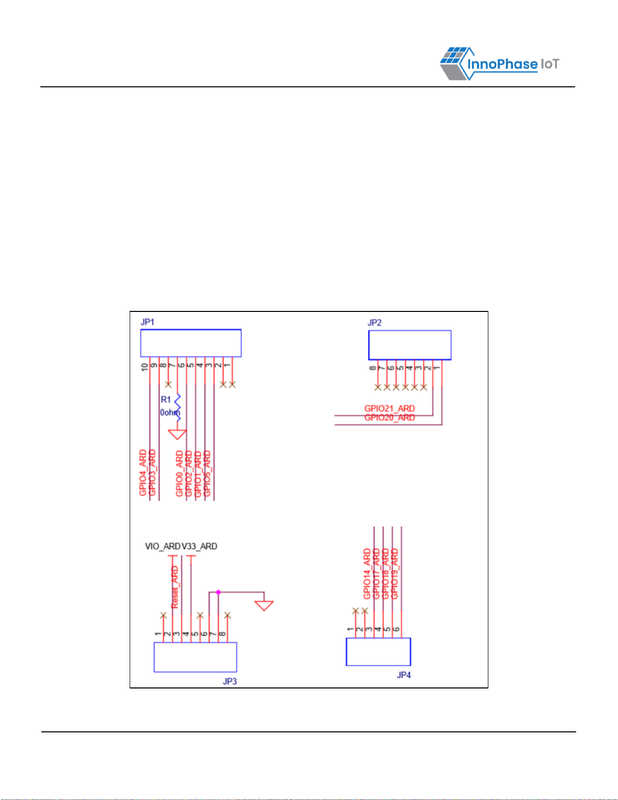
Shield Headers (JP1 to JP4)
Arduino UNO compatible headers are available in the INP301x board to interface with any compatible host
micro-controller.
The GPIOs assigned to shield headers are carefully chosen to achieve following capability:
1. INP101x’s SPI slave pins available on JP1
2. INP101x’s I2C master pins available on JP1
3. Remaining GPIOs are available on JP2 and JP4
Note that INP301x supports 2.5V IO as the default configuration. The shield header connections are as shown
in JP2 of Figure 6.
Figure 6: Arduino UNO shield compatible jumpers
Talaria TWO Evaluation & Development Kit
Version 5.0 Copyright © | All Rights Reserved | Proprietary 12
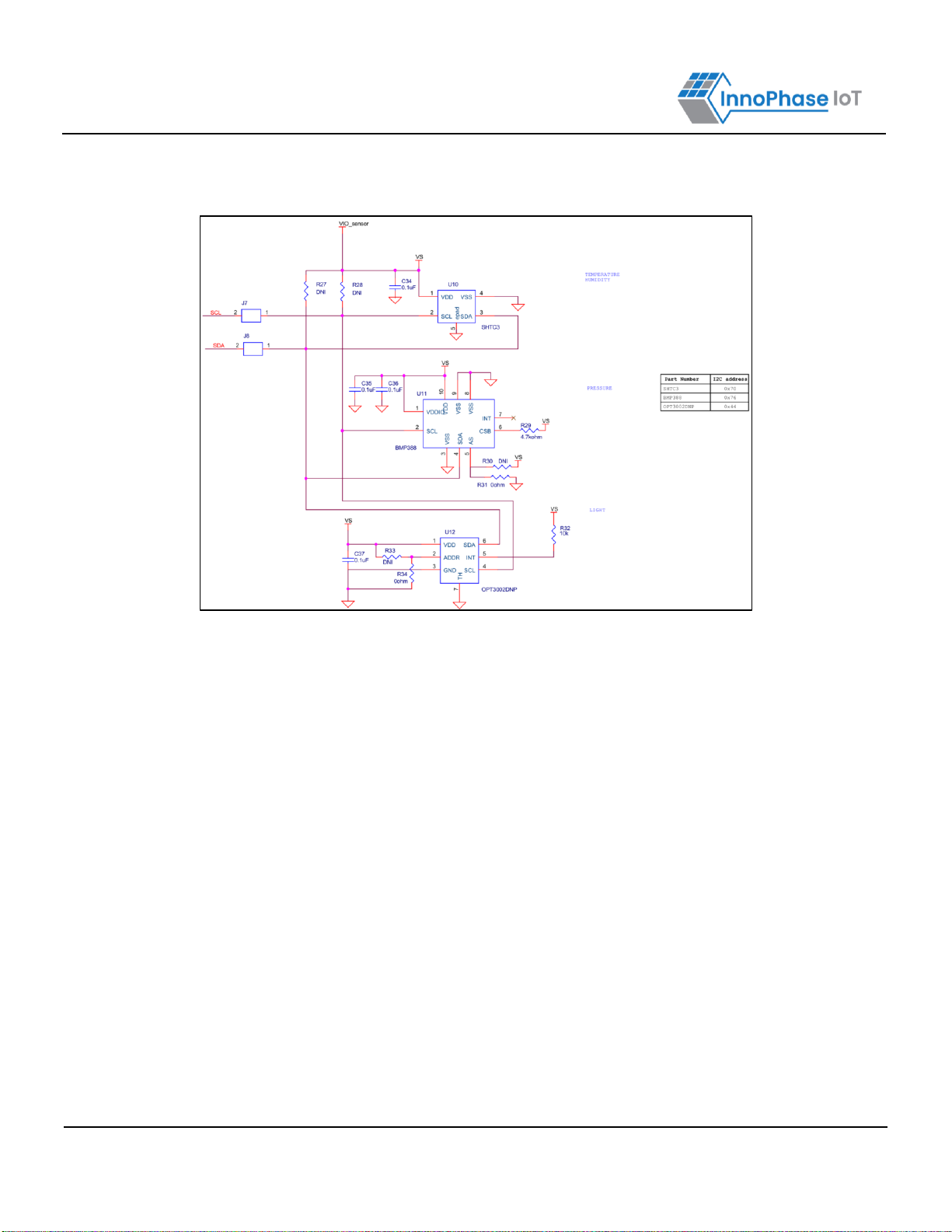
On Board Sensors
Figure 7: On board sensors
The INP301x board has following sensors available on board for quick prototyping/testing:
1. Temperature/Humidity (Sensirion SHTC3)
2. Pressure (Bosch BMP388)
3. Light (TI OPT3002)
To use the sensors, J7, J8, pins 1 & 2 of J1 should be connected. This enables power connection to the
sensors on board, I2C connection on GPIOs 3 & 4.

Talaria TWO Evaluation & Development Kit
Version 5.0 Copyright © | All Rights Reserved | Proprietary 13
Functional Description
Following are the functional modes that can be achieved in the INP301x board:
1. Stand-alone mode (host-less)
2. Shield mode (hosted)
More details about each mode are available in subsequent sections. Switching between the modes is handled
by DPDT switch U3 for power, and multi-port SPDT switch U1 for the GPIOs.
Stand-alone Mode
The stand-alone mode is intended for following use cases:
1. Host-less application development on INP101x modules
2. Programing access to INP101x modules
In stand-alone mode, the U3 switch is pushed towards pin 3, which disconnects power and IO from shield
headers and connects them to FTDI. The FTDI port layout is shown in Table 2.
FTDI Bus
Interface to Talaria TWO
A
JTAG
B
RESET
C
UART
D
CONSOLE (UART)
Table 2: FTDI Layout
The A & B bus of FTDI device supports MPSEE protocol, hence JTAG is assigned to A-bus. The BDBUS7 is
connected EN_CHIP of the INP101x module. The C & D bus of FTDI device used as UARTs, with C-bus
connected to peripheral UART of INP101x module and D-bus connected is CONSOLE port (GPIO17) of INP101x
module.
The JTAG on A-bus is used for debugging applications on the INP101x module. The UART on C-bus is used for
programming the INP101x module. The CONSOLE port is a unidirectional UART from INP101x module that
operates at high baud rate of 2457600, used for debug prints.
Talaria TWO Evaluation & Development Kit
Version 5.0 Copyright © | All Rights Reserved | Proprietary 14
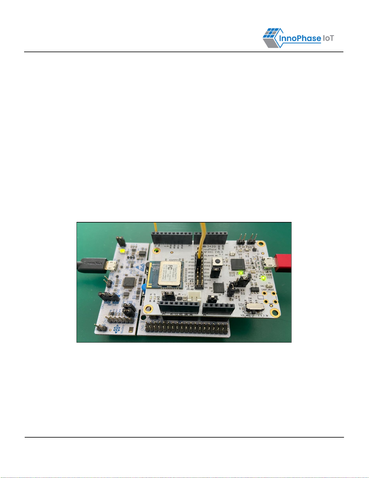
Shield Mode
This mode will make the EVB-A board to act as a Wi-Fi/BLE5 shield. To enable this mode, flip the switch U3
towards V33_ARD. This also pulls up the INA pinof the multi-port SPDT device MAX4761ETX, which then routes
the GPIOs from the INP101x module to the shield headers JP1, JP2, JP3 and JP4. In the shield mode a suitable
firmware (such as Serial to Wi-Fi application available in the SDK) should be pre-flashed in the INP101x.
EVB-A as Wi-Fi Shield with STM32 Nucleo Board
A comprehensive set of host application packages are available to download via the InnoPhase website to
demonstrate the use of EVB-A as a Wi-Fi/BLE5 shield board.
Mount the Talaria TWO EVB on the STM32 board on Arduino connector. Connect GPIO4 of Talaria TWO (J1
Connector) to Pin2 of CN6 connector. Talaria TWO uses this GPIO4 pin tointerrupt ST when Talaria TWO wants
to send data/notification to ST.
Figure 8: INP3010 EVB-A as Wi-Fi Shield
Talaria TWO Evaluation & Development Kit
Version 5.0 Copyright © | All Rights Reserved | Proprietary 15
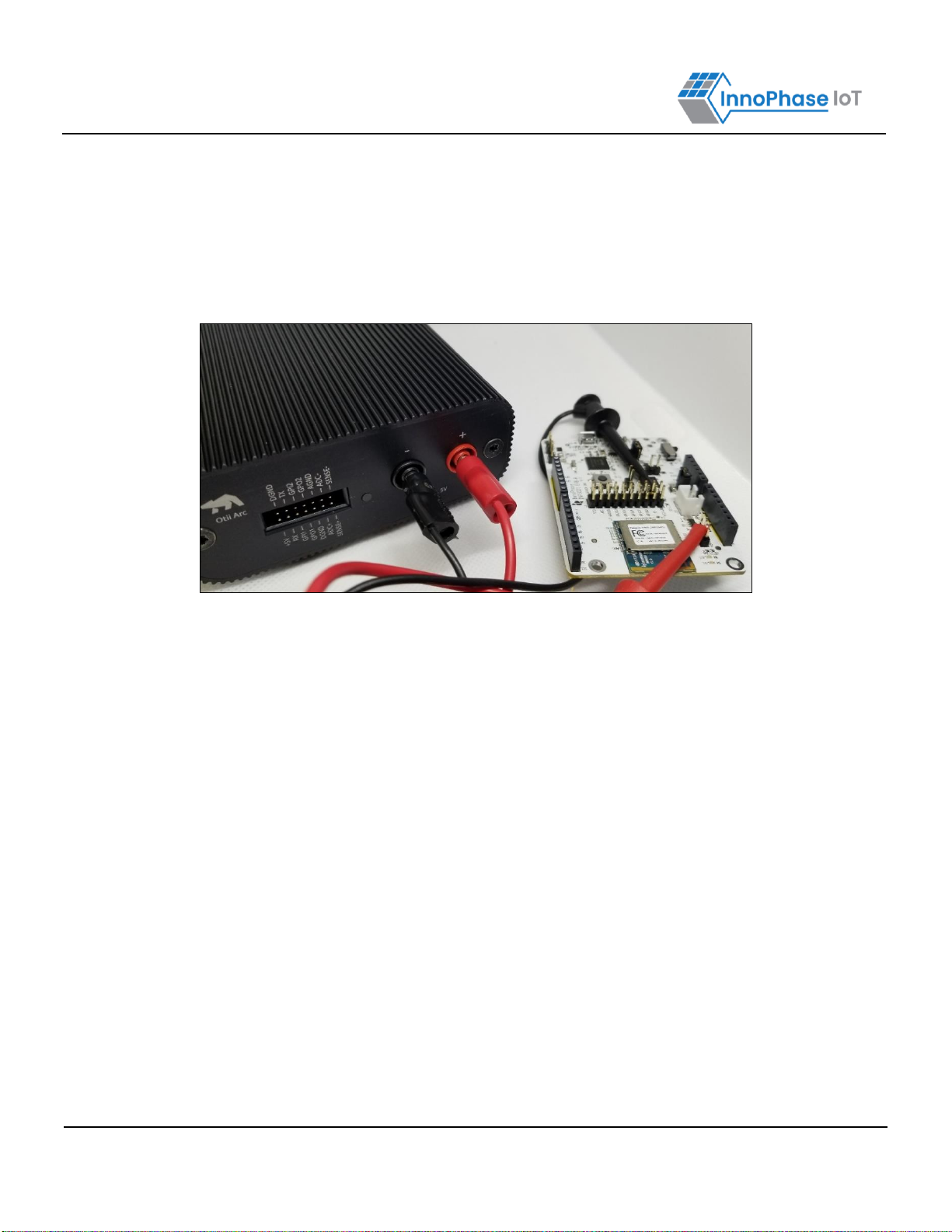
Power Measurement
The power consumption of the INP101x module is measured by either connecting a DMM on the jumper J4 or
supplying power directly on J4 using specialty power supplies like Otti Arc from Qiotech. Figure 9 shows the
connection setup to measure current consumption using Otti Arc.
Figure 9: Current measurement setup using Otti Arc
Talaria TWO Evaluation & Development Kit
Version 5.0 Copyright © | All Rights Reserved | Proprietary 16
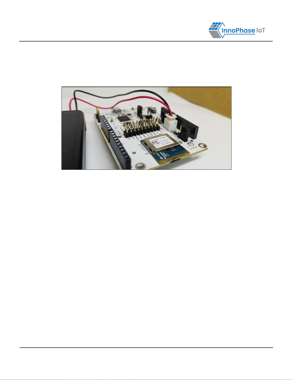
Using Battery as Power Source
Header J4 will switch between VBat and Vm_3.3V. Figure 10 shows VBat connection.
Figure 10: J10 Battery connection
Note: When using a battery as a power source there will be an additional current draw from LED (D7 or D12
depending on board version). If attempting to measure an accurate module current draw from the battery
connection, the LED series resistor must be removed to disconnect the LED.
Talaria TWO Evaluation & Development Kit
Version 5.0 Copyright © | All Rights Reserved | Proprietary 17
Antenna
The antennas integrated with INP2045 are listed in Table 3 have been approved for FCC/ISED, EU(RED) and
TELEC.
Module ID
Antenna Type
Model Number
Antenna
Manufacturer
Max Peak Antenna
Gain (dBi)
INP1010
PCB Antenna
INP1010 PCB TRACE
InnoPhase
0.9
INP1011
SMA Antenna (External
Antenna)
W24-ASMA-M
Inventek
2.15
INP1012
SMA Antenna (External
Antenna)
W24-ASMA-M
Inventek
2.15
INP1013
SMD Chip Antenna
2450AT42B100
Johanson
0
INP1014
PCB Antenna
1014 PCB Trace
InnoPhase
5.33
INP1015
SMA Antenna (External
Antenna)
W24-ASMA-M
Inventek
2.15
Table 3: Module ID with Antenna details
INP1010
Talaria TWO INP1010 module has a proprietary integrated/printed antenna. It is a Double-sided Inverted F
(IFA) antenna and has been implemented as printed PCB elements.
By design and verification, Antenna does not require any additional matching component if the module is used
as standalone product. This INP1010 PCB antenna integrated with INP2045 has been approved for
FCC/ISED, EU(RED) and TELEC.
Module ID
Antenna Type
Model Number
Max Peak Antenna Gain (dBi)
INP1010
PCB Antenna
INP1010 PCB TRACE
0.9
Table 4: INP1010 - Antenna specifications
INP1011/INP1012/INP1015
Talaria TWO INP1011/INP1012/INP1015 module has been certified with External SMA antenna W24-ASMA-
M which has been approved for FCC/ISED, EU(RED) and TELEC.
Module ID
Antenna Type
Model Number
Max Peak Antenna Gain (dBi)
INP1011/012/015
SMA Antenna (External
Antenna)
W24-ASMA-M
2.15
Table 5: INP1011/012/015 - Antenna specifications

Talaria TWO Evaluation & Development Kit
Version 5.0 Copyright © | All Rights Reserved | Proprietary 18
INP1013
Talaria TWO INP1013 module has been certified with SMD chip antenna 2450AT42B100 which has been
approved for FCC/ISED and TELEC.
Module ID
Antenna Type
Model Number
Max Peak Antenna Gain (dBi)
INP1013
SMD chip antenna
2450AT42B100
0
Table 6: INP1013 - Antenna specifications
INP1014
Talaria TWO INP1014 module has a proprietary integrated/printed PCB antenna. By design and verification,
antenna does not require any additional matching components if the module is used as a stand-alone product.
INP1014 PCB antenna integrated with INP2045 has been approved for FCC/ISED and TELEC.
Module ID
Antenna Type
Model Number
Max Peak Antenna Gain (dBi)
INP1014
PCB Antenna
1014 PCB Trace
5.33
Table 7: INP1014 Antenna specifications

Talaria TWO Evaluation & Development Kit
Version 5.0 Copyright © | All Rights Reserved | Proprietary 19
FCC/ISED Regulatory Notices
Modification Statement
Changes or modifications made to this equipment not expressly approved by InnoPhase IoT, Inc. may void the
FCC authorization to operate this equipment.
Interference Statement
This device complies with Part 15 of the FCC Rules and with Industry Canada license-exempt RSS
standard(s). Operation is subject to the following two conditions:
1. this device may not cause harmful interference, and
2. this device must accept any interference received, including interference that may cause undesired
operation
Le présent appareil est conforme aux CNR d'Industrie Canada applicables aux appareils radio exempts de
licence. L'exploitation est autorisée aux deux conditions suivantes:
1. l'appareil ne doit pas produire de brouillage, et
2. l'appareil doit accepter tout brouillage radioélectrique subi, même si le brouillage est susceptible d'en
compromettre le fonctionnement
Radio Frequency Radiation Exposure Statement
This device complies with FCC/IC radiation exposure limits set forth for an uncontrolled environment.
The device should be installed and operated with minimum distance of 20 CM between the device/antenna and
all persons. This device must not be co-located or operating in conjunction with any other antenna or transmitter
without further RF Exposure evaluation.
RF Exposure Statement for Module Integration
Talaria TWO modules listed above have been granted modular approval for mobile applications. Host products
integrators may use the module in their final products with the same antenna without additional FCC certification
if they meet the following conditions. Otherwise. additional FCC approvals must be obtained.
1. The host product with the module installed must be evaluated for simultaneous transmission
requirements
2. The user manual for the host product must clearly indicate the operating requirements and conditions
that must be observed to ensure compliance with current FCC IC RF exposure guidelines.

Talaria TWO Evaluation & Development Kit
Version 5.0 Copyright © | All Rights Reserved | Proprietary 20
Support
1. Sales Support: Contact an InnoPhase sales representative via email –sales@innophaseiot.com
2. Technical Support:
a. Visit: https://innophaseiot.com/contact/
b. Also Visit: https://innophaseiot.com/talaria-two-modules/
c. Contact: support@innophaseiot.com
InnoPhase is working diligently to provide customers outstanding support to all customers.
Other manuals for Talaria TWO INP3010
1
This manual suits for next models
5
Table of contents
Other Innophase Motherboard manuals

Popular Motherboard manuals by other brands


Geniatech
Geniatech DB8 manual

Quantum Design
Quantum Design ZillioX 6 manual

Silicon Laboratories
Silicon Laboratories Si84xxISO user manual

International Rectifier
International Rectifier IRDC3847-P1V2 user guide

Microchip Technology
Microchip Technology MCP19117 user guide

GIGAIPC
GIGAIPC ATX-Q670A user manual


