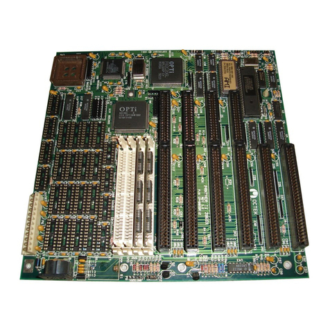
Octek Hippo COM User manual

HIPPO COM

The material in this manual is for information only and is subject to change without notice.
REVISION: 1.1
IBM, IBM PC/XT/AT, PC-DOS, MS-DOS, OS/2, INTEL, AMI ARE THE
TRADEMARKS OR REGISTERED TRADEMARKS OF THEIR RESPECTIVE
OWNERS.

RADIO FREQUENCY INTERFERENCE STATEMENT
This equipment generates and uses radio frequency energy and if not
installed and used properly, that is, in strict accordance with the
manufacturer's instructions, may cause interference with radio and
television reception.
If this equipment does cause interference to radio or TV reception, which
can be determined by turning the equipment off and on, the user is
encouraged to try to correct the interference by one or more of the
following measures:
* Reorient the receiving antenna.
* Relocate the computer away from the receiver.
* Move the computer away from the receiver.
*Plug the computer into a different outlet so that computer and receiver
are on different branch circuits.
*Ensure that card slot covers are in place when no card is installed.
*Ensure that card mounting screws, attachment connector screws, and
ground wires are tightly secured.
*If peripherals are used with this system, it is suggested to use shielded,
grounded cables, with in-line filters if necessary.
If necessary, the user should consult the dealer service representative for
additional suggestions.
The manufacturer is not responsible for any radio or TV interference
caused by unauthorized modifications to this equipment. It is the
responsibility of the user to correct such interference.

Note
1.Electronic components are sensitive to dust and dirt. Do inspect and
clean the computer system regularly.
2.Turn off the power whenever you install or remove any connector,
memory module and add-on card. Before turning on the
power, make sure that all the connectors, memory modules and
add-on cards are secured.
3.After power is on, wait for a minute. The system BIOS are going
through a self-test during this period and nothing is shown on
the screen. After the self-test, the system BIOS will initialize the
display adaptor and show messages.
4.The SIMM sockets are fragile device. Do not force the SIMM modules
into the sockets. It may break the locking latches.

Preface
The manual provides information about the installation and
maintenance of HIPPO COM motherboard. In-depth explanations of
the functions of this motherboard are provided. In the appendix, the
system BIOS setup is explained.
The content in this manual is only for reference and is intended
to provide the basic information for the general users. There are also
technical information for hardware and software engineers.
In this manual, there are 4 chapters. Chapter 1 contains a brief
introduction and specification of HIPPO COM motherboard. In the
Chapter 2, the functions of HIPPO COM are explained. It also
outlines many advanced features of the CPU and the system architecture.
Chapter 3 explains the installation of coprocessor, DRAM modules and
jumpers. Technical information is provided in the Chapter 4.
System BIOS is described in the attached BIOS Manuaw

Table of Content
Chapter 1 INTRODUCTION
Chapter 2 GENERAL FEATURES
Specification 2-1
Chapter 3 CONFIGURING THE SYSTEM
Installing RAM Modules 3-1
Configuration of Memory 3-2
DRAM Configuration 3-3
Control of System Speed 3-4
System Board Jumper Setting 3-5
System Board Connectors 3-9
Chapter 4 TECHNICAL INFORMATION
Memory Mapping 4-1
I/O Address Map 4-2
System Timers 4-4
System Interrupts 4-6
Direct Memory Access (DMA) 4-7
Real Time Clock and CMOS RAM 4-8
CMOS RAM Address Map 4-9
Real Time Clock Information 4-10
System Expansion Bus 4-11

Appendix A OPERATION AND MAINTENANCE
Static Electricity A-1
Keeping The System Cool A-1
Cleaning The `Golden Finger' A-2
Cleaning The Motherboard A-2
Appendix B SUMMERY OF JUMPER SETTING
Appendix C SYSTEM BOARD LAYOUT


_________________________________________________________________________
1
-
1
Chapter 1
Introduction
___________________________________________________________
HIPPO COM is designed to be a powerful platform for
sophisticated software available now and in the future. It contains the
most powerful microprocessor 80486 which combines CPU, numeric
coprocessor and internal cache memory on a single chip. HIPPO COM
fully takes advantage of the power of 80486 and provides high
performance, reliability and compatibility to the user.
Fast A20 gate and fast reset generation are incorporated to
improve the performance of advanced operation system and expanded
memory managers.
Compatibility and reliability are important issues. I/O channel
is compatible to standard AT bus and any peripheral may be used.

INTRODUCTION
__________________________________________________________________________
_________________________________________________________________________
1
-
2
THE PAGE IS INTENTIONALLY LEFT BLANK

_________________________________________________________________________
2
-
1
Chapter 2
General Features
___________________________________________________________
SPECIFICATION
Processor :
Intel 80486DX, 80486DX2, 80486SX or 80487SX CPU
Speed :
Turbo/normal speed
I/O Slot :
Compatible to standard AT bus
Four 16-bit slots
Memory :
Shadow RAM for system and video BIOS
Page mode and hidden refresh
Flexible configuration
SIMM sockets for 256KB, 1MB or 4MB modules

GENERAL FEATURES
_________________________________________________________________________
_________________________________________________________________________
2
-
2
Cache :
8KB four way set associative internal cache
System Support Functions :
- 8-Channel DMA (Direct Memory Access)
- 16-level interrupt
- 3 programmable timers
- CMOS RAM for system configuration
- Real time clock with battery back-up
- Fast A20 gate and fast reset
Other Features :
- External battery connector

GENERAL FEATURES
_________________________________________________________________________
_________________________________________________________________________
2
-
3
PROCESSOR
The power of HIPPO COM comes from 80486. 80486 is the
state-of-art microprocessor which merges many innovative features on a
single chip for advanced applications and operation systems. Fabricating
with the 1um process, this CPU consists of more than one million
transistors. With such high density, this CPU incorporates as many as
new features to make itself the most powerful microprocessor.
80486 is a 32-bit microprocessor with 32-bit external data bus
and 32-bit external address bus. It not only contain a central processing
unit, but also integrates a numeric processor and a four-way set associate
cache memory. It is fully binary compatible with 80386 and 80387. All
existing software for PC XT/AT can be used on HIPPO COM. However,
due to the new internal architecture, the performance of 80486 is two to
four times of 80386.
Cache memory can improve the overall performance of a
computer system. Nevertheless, if the cache memory is separated from
CPU, CPU still needs to fetch code and data through external bus. That
means the data transfer rate should not be too fast so that the external
devices are able to keep pace with the CPU. In 80486, the cache
controller and cache memory are integrated into the chip. Most of the
operations can be carried out inside the CPU, which reduces the bus
operations on external data and address bus and thus speeds up the
internal execution.

GENERAL FEATURES
_________________________________________________________________________
_________________________________________________________________________
2
-
4

GENERAL FEATURES
_________________________________________________________________________
_________________________________________________________________________
2
-
5

GENERAL FEATURES
_________________________________________________________________________
_________________________________________________________________________
2
-
6
The cache memory is a 8K bytes, 16 bytes line size, four-way
set associative configuration. The hit rate of this configuration is much
better than 32K bytes two-way set associative external cache because a
four-way set associative architecture provides better performance in a
multitasking and multi-processor environment.
Bus snooping feature keeps the cache memory consistent with
the main memory. When an external processor overwrites the content in
the main memory, the corresponding data in the internal cache memory
will be invalidated and will be fetched from main memory when CPU
reads this data.
If a read miss occurs, the CPU will initiate a burst mode read
operation. In burst mode read operation, CPU performs four successive
read operations each of which takes only one cycle. Total 128 bits data
are fetched into the CPU's internal cache. Since burst mode read
operation is very fast, the traffic of the CPU bus is greatly reduced and
the bus is available to other bus masters, such as DMA controller.
Reading 128 bits data into CPU will take some times. In order
to reduce the delay, the internal cache controller works parallel with
CPU. It fetches the data needed by CPU for the present operation and
the CPU read cycle is terminated. Then the other data are read into the
internal cache memory while CPU is doing something else. This
arrangement permits the CPU to run at zero wait state.

GENERAL FEATURES
_________________________________________________________________________
_________________________________________________________________________
2
-
7
By eliminating the access to external bus, operations with the
internal cache can be completed in a single cycle. 80386 at least needs
two cycles for an operation. To further increase the rate of data transfer
inside the CPU, the internal bus of the cache memory is increased to 128
bits, which is four times of the external bus. Since, in most of the time,
the CPU is using the internal cache, the large bus size substantially
improves the overall performance.
When the CPU writes data to the main memory, the data is first
stored in a write buffer. There are four write buffers. When the
external bus is idle, data will be sent to the main memory. If all buffers
are filled, it can start write operation in burst mode. Since the internal
cache is updated immediately, the CPU need not suspend its operation
and there is no need to wait for the external device to update the main
memory.
Many often-used instructions are executed in a clock cycle and
some instructions are modified to take fewer cycles than in 80386. On
the contrary, 80386 may take two to three more cycles for the same
instruction. The CPU contains an advanced instruction pipeline structure
and a 32-byte code queue to speed up the execution.
80486 includes all the functions of 80386 and is able to support
sophisticated software and operation systems which are widely employed
now. It is able to operate in real mode, protected mode and virtual 8086
mode.

GENERAL FEATURES
_________________________________________________________________________
_________________________________________________________________________
2
-
8
Internal memory management unit provides a flexible
addressing scheme for the next generation operation system.
Multitasking, concurrent operation and manipulating huge data base can
be accomplished with excellent performance. Paging mechanism is
employed to allow powerful operating system to implement virtual
memory. Each segment is divided into several pages which are 4K bytes
per page. Page mechanism is transparent to software and allows
software to address 64 terabytes. Furthermore, the 64KB segment
boundary which is an barrier of 8088 and 80286 is removed and the
segment length can be increased up to 4GB.
The demand for sophisticated, number-crunching scientific and
business applications has rapidly increased in recent years. In the past,
microprocessor features an integer Arithmetic Logic Unit which only
handles simple integer operations such as addition and multiplication.
Floating-point operations which are actually utilized by applications must
be accomplished through software routines.
To meet the demand of floating-point calculation, a numeric
coprocessor is necessary. However, an external coprocessor has been
found to be the bottleneck of data transfer. 80486 integrates the
coprocessor on chip and thus the data transfer to external bus is
eliminated. The on-chip coprocessor is compatible with 80387. It
works parallel with other units in the CPU, which results in a better
performance of numeric process.

GENERAL FEATURES
_________________________________________________________________________
_________________________________________________________________________
2
-
9
MEMORY SYSTEM
Two banks of DRAMs can be installed on board. So 8 SIMM
modules may be installed on your system and the maximum memory size
is up to 64MB. 256KB, 1MB, 4MB & 16MB DRAM SIMM modules
are supported. The DRAM should be fast-page mode DRAM with
staggered refresh capability.
The memory system provides a flexible memory configuration.
Several combinations of DRAM types are allowed. The DRAM type
and the memory size are automatically detected by the system BIOS.
So, you may easily change the configuration of the system.
The memory controller system supports fast
page mode. The memory is divided into pages with equal size.
Successive memory accesses within the same page need not require wait
state. Furthermore, a burst line fill mode is implemented. In case of a
read miss of cache memory, 16 bytes data will be fetched from main
memory to cache memory. Using page mode operation will speed up the
line fill operation.To enhance the system performance, shadow RAM
mode is supported. In shadow RAM mode, system BIOS and video
BIOS contained in low speed memory such as EPROM and ROM are
copied into DRAM. Improvement is significant because access to
DRAM is mush faster than ROM.

GENERAL FEATURES
_________________________________________________________________________
_________________________________________________________________________
2
-
10
The memory refresh logic is redesigned to improve the system
performance and power consumption. In the original PC/AT design, the
memory refresh operation will suspend the CPU operation because it has
to access the main memory. In a high speed system like HIPPO COM,
the CPU indeed can process a large amount of operations in the memory
refresh period.
By implementing hidden refresh method, the refresh operations
for expansion card on the AT bus and for the main memory are separated.
To be compatible, the refresh operation for AT bus will not be changed.
But the refresh operation for main memory will be carried out
individually and will be done when there is no access to main memory.
Furthermore, the frequency of the main memory refresh operation may be
set to 'normal' or 'slow'. All types of DRAM can be used in `normal'
mode. When 'slow' mode is selected, the availability of main memory is
increased but the refresh period of DRAM should be longer. Since the
refresh period of DRAM from different manufacturers may vary, consult
your dealer for detail.
Table of contents
Other Octek Motherboard manuals

Octek
Octek RHINO 5 User manual

Octek
Octek RHINO VAP133-ACP User manual

Octek
Octek HIPPO PRO 486 User manual

Octek
Octek HIPPO DCA 2 User manual

Octek
Octek P4X266A-A4E User manual

Octek
Octek Panther II User manual

Octek
Octek Hippo-SX User manual

Octek
Octek HAWK 486 User manual

Octek
Octek Panther-II 386SX User manual

Octek
Octek FOX-II User manual