Intellec Series II Operating and maintenance manual

INTELLEC®
SERIES
II
MICROCOMPUTER
DEVELOPMENTSYSTEM
HARDWARE
REFERENCEMANUAL
ManualOrder
No.
9800556-02
Rev.
B
Copyright
©
1978,1980
IntelCorporation
J
Intel
Corporation,
3065
BowersAvenue,SantaClara,California
95051
L
_
Additional
copies
of
thismanual
or
other
Intel
literature
maybe
obtained
from:
Literature
Department
Intel
Corporation
3065BowersAvenue
Santa
Clara,
CA
95051
The
information
in
thisdocument
is
subject
to
change
without
notice.
Intel
Corporationmakes
no
warranty
ofany
kind
with
regard
to
this
material,
including,
butnot
limited
to,the
impliedwarranties
of
merchantability
and
fitness
fora
particularpurpose.
Intel
Corporation
assumes
no
responsibility
forany
errorsthat
may
appear
in
thisdocument.
Intel
Corporationmakes
no
commitment
to
update
norto
keepcurrent
the
informationcontained
in
this
document.
Intel
Corporationassumes
no
responsibility
fortheuseofany
circuitryotherthan
circuitry
embodied
in
an
Intel
product.
No
othercircuitpatentlicenses
are
implied.
Intel
softwareproducts
are
copyrighted
byand
shallremain
the
property
of
Intel
Corporation.Use,
duplication
or
disclosure
is
subject
to
restrictionsstated
in
Intel'ssoftwarelicense,
oras
defined
in
ASPR
7-104.9(a)(9).
No
part
of
thisdocument
maybe
copied
or
reproduced
inany
form
orbyany
means
without
the
prior
written
consent
of
IntelCorporation.
The
following
are
trademarks
of
Intel
Corporation
andmaybe
usedonly
to
identify
Intel
products:
BXP
Intellec
Multibus
i
iSBCMultimodule
ICE
iSBX
PROMPT
iCS
LibraryManager
Promware
Insite
MCSRMX
Intel
Megachassis
DPI
Intelevision
Micromap
^Scope
andthe
combination
of
ICE,iCS,
iSBC,
iSBX,
MCS,
orRMXanda
numerical
suffix.
11
A1016/783/1K
DD

PREFACE
Thismanualdescribes
hardware
and
softwareelements
ofthe
IntellecSeries
II
MicrocomputerDevelopmentSystems
as
necessary
to
delineateinternal
processes
and
dataflow.
The
information
is
intended
to
supporthardwaretroubleshooting
andto
provide
a
basis
for
understanding
the
development
system's
resources.
Informationwithin
thesix
chapters
of
thismanual
isas
follows:
r
•
General
Information—Descriptions
ofthe
threebasicmodels(Model220,
225
and
230)
and
optionalhardware
and
softwarefeatures.
An
overview
ofthe
functional
organization
anda
review
ofthe
primaryintersystemcommunica-
tions
path
(theMultibusinterface).
•
Integrated
Processor
Board
(IPB)—A
technicaldescription
ofthe
circuit
elementscomprising
the
8080-based
data
processing
and
controlcenter
ofthe
Intellec
Series
II
developmentsystem.
•
Integrated
Processor
Card
(IPC)—A
technicaldescription
ofthe
circuit
elementscomprising
the
8085-based
data
processing
and
controlcenter
ofthe
Intellec
Series
II
developmentsystem.
•
Input/Output
Controller
(IOC)—A
technicaldescription
ofthe
circuit
elements
thatestablish
an
intelligent
interfacebetween
the
IPB
or
IPC
andthe
integral
CRTand
diskettedrive.
•
Parallel
Input-Output
(PIO)
Subsystem—A
technicaldescription
ofthe
circuit
elements
thatestablish
an
intelligent
interfacebetween
theIPBorIPCandthe
standardIntellecSeries
II
developmentsystemperipherals(papertape
reader/punch,printer
and
PROM
programmer).
•
Keyboard
Assembly—A
technicaldescription
ofthe
circuit
elementsthatdetect
and
decode
keystrokes
and
keystrokecombinationsenteredfrom
the
keyboard.
Informationwithinthismanualdescribes
LSIandTTL
chipsonly
tothe
extent
necessary
to
supporttroubleshooting
tothe
circuit
board
level.Furtherdetails
on
the
chips
are
provided
by
chipmanufacturerliteratureincluding
the
following
Intel
manuals:
•In
tel
Component
Data
Ca
talogue
•
MCS-80/85
Family
User's
Manual,
OrderNumber121506
Although
the
informationherein
is
intended
to
supporthardwaremaintenance,
the
manual
does
not
containmaintenanceprocedures
or
guidelines.Maintenance
information
is
provided
inthe
following
manuals:
•
Intellec
Series
II
Microcomputer
Development
System
Schematic
Drawings,
Order
Number
9800554
•
Intellec
Series
II
Microcomputer
Development
Systems
Models
220,
221,
222
and
Models
230, 231,
232
Service
Information,
Order
Number
9800878
•
Intellec
Series
II
Microcomputer
Development
Systems
Models 225, 226,
227
Service
Information,
Order
Number
121569
Intellec
Series
IIis
compatiblewith
a
variety
of
optionalperipheraldevices
and
circuit
boards.
Technicaldetails
onthe
IntellecSeries
II
developmentsysteminter-
face
with
any
suchdevice
or
board
are
provided
inthe
associatedtechnicalmanual.
Non-standarddevices
and
boards,
whichrequiremodification
ofthe
IntellecSeries
II
developmentsystemhardware
or
software,void
the
developmentsystemwarranty
111
unless
priorwrittenapproval
is
obtained
from
IntelCorporation.Guidelines
forthe
use
of
non-standard
devices
and
modifications
to
meet
unique
user
needs
are
pro-
vided
inthe
following
manual:
Intellec
Series
II
Microcomputer Development System Hardware
Interface
Manual,
OrderNumber9800555
-
Other
manualsthatsupport
useofthe
Intellec
Series
II
development
systems
are:
•
/5/S-//
User's
Guide,
OrderNumber9800306
•
Intellec Series
II
Model 22X/23X Installation
Manual,
Order
Number
9800559
•
Intellec Series
II
Microcomputer Development Sytem Monitor
Listings,
Order
Number
9800605
,
.
_
IV

CONTENTS
CHAPTER
1
PAGE
GENERAL
INFORMATION
DevelopmentSystemModels
1-1
FunctionalOrganization
1-2
Multibus
Architecture
1-3
Options
1-4
ExpansionChassis
1-6
Universal
PROMProgrammer
1-6
In-Circuit
Emulators
1-6
High-Level
Languages
1-6
IPC
Upgrade
Kit1-6
Disk
Drives
1-6
Specifications
1-7
CHAPTER
2
INTEGRATED
PROCESSOR
BOARD
MasterProcessorSubsystem
2-1
MasterProcessor
and
ClockGenerator
2-1
SystemController
2-3
Bus
Controller
2-3
Bus
Acquisition
2-3
Bus
Release
2-4
Bus
Override
2-4
Bus
ControlCycle
2-4
Bus
PriorityResolutionLogic
2-5
IPB
MemorySubsystem
2-5
IPBROM
2-5
IPBRAM2-7
External
ROMandRAM2-8
IPB
Input-OutputSubsystem
2-8
Interrupt
RequestCircuits2-12
External
(PIO/IOC)
I/O
Control
Circuits2-13
Internal
I/O
ControlCircuits2-13
CHAPTER
3
INTEGRATED
PROCESSOR
CARD
Master
Processor
Subsystem
3-1
MasterProcessor
3-1
Bus
Controller
3-4
Bus
Acquisition
3-4
Bus
Release
3-4
Bus
Override
3-5
Bus
ControlCycle
3-5
Bus
PriorityResolutionLogic
3-6
PAGE
Memory
Subsystem
3-6
IPCROM3-6
IPCRAM3-8
IPC
Input-OutputSubsystem3-10
External
(PIO/IOC)
I/O
Transfers3-10
Internal
I/O
Transfers3-12
Interrupt
RequestCircuits3-13
CHAPTER
4
INPUT-OUTPUT
CONTROLLER
IOC
ProcessorSubsystem
4-2
IOC
Processor
and
ClockGenerator
4-2
Reset
Logic
4-3
DMA
Controller
4-4
IOC
MemorySubsystem
4-6
IOCROM4-7
IOCRAM4-7
IOC
Input-OutputSubsystem
4-8
IOC
Port
Decode
Logic
4-8
Miscellaneous
Input/OutputCircuits4-10
IOC
IntervalTimer4-10
DataByte
Buffer
4-10
Keyboard
InputCircuits
4-11
CRT
ControlCircuits
4-11
Diskette
ControlCircuits
.
4-15
CHAPTER
5
PARALLEL
INPUT-OUTPUT
SUBSYSTEM
PIO
Processor
5-2
PIO-IPB/IPC
Interface
5-2
PeripheralDeviceInterface
5-2
CHAPTER
6
KEYBOARD
ASSEMBLY
Principles
of
Operation
6-1
KeyboardElectronics
6-2

TABLES
_
TABLE
1-1
1-2
1-3
1-4
1-5
TITLE
PAGE
2-1
Multibus
Interface
Pin
Assignments
1-4
Multibus
Interface
SignalDescriptions
1-5
Drive
OptionApplicability
1-7
Intellec
Series
II
Microcomputer
DevelopmentSystemSpecifications
1-7
SystemChassis
and
OptionalExpansion
ChassisPowerSupplyCurrent
Capabilities
1-9
Bus
RequestMachineCycles
2-3
TABLE
TITLE
PAGE
2-2
ROM
EnableLatchDecoding
2-7
2-3
Port
Address/ControlSignalList2-15
3-1
Control
Port
Decoding
3-8
3-2
RAM
ControlLogicOperation
3-9
3-3
I/O
Port
AddressDecoding
3-11
4-1
Port
AddressFunctions
4-9
5-1
AddressDecoding
for
PeripheralDevice
ControlSignals
5-3
5-2
DeviceStatusByteFormat
5-4
.
ILLUSTRATIONS
FIGURE
TITLE
1-1
1-2
1-3
2-1
2-2
2-3
2-4
2-5
2-6
2-7
2-8
2-9
3-1
3-2
Models
220and225
Model
230
Intellec
Series
II
Microcomputer
DevelopmentSystemBlockDiagram
.
IPB
SimplifiedBlockDiagram
Master
Processor
SubsystemBlock
Diagram
Bus
AcquisitionTiming
Bus
Control
CycleTiming
IPB
MemorySubsystemBlockDiagram
RAM
RefreshCycleTiming
RAM
ReadCycleTiming
RAM
WriteCycleTiming
IPB
I/O
SubsystemBlockDiagram
IPC
Simplified
BlockDiagram
Master
Processor
SubsystemBlock
Diagram
PAGE
1-1
1-1
1-2
2-2
2-2
2-4
2-5
2-6
2-8
2-9
2-10
2-11
3-2
3-3
FIGURE
TITLE
PAGE
3-3
3-4
3-5
3-6
3-7
4-1
4-2
4-3
4-4
4-5
4-6
4-7
4-8
5-1
Bus
AcquisitionTiming
3-4
Bus
ControlCycleTiming
3-5
IPC
MemorySubsystemBlockDiagram
....
3-7
RAM
AccessCycle
3-9
IPCI/O
SubsystemBlockDiagram3-10
IOC
Simplified
BlockDiagram
4-1
IOC
ProcessorSubsystemBlockDiagram
...
4-3
IOC
MemorySubsystemBlockDiagram
....
4-6
IOCRAM
Timing
4-7
IOCI/O
SubsystemBlockDiagram
4-9
CharacterDisplayMatrix4-12
Dot
PatternTiming4-13
CRT
SweepTiming4-14
PIO
BlockDiagram
5-1
_
VI
CHAPTER
1
GENERAL
INFORMATION
The
IntellecSeries
II
MicrocomputerDevelopment
Systems
are
bus-oriented,multiprocessorsystems
thatemployROM-based
as
well
as
diskette-based
software.
Each
development
systemwithin
the
series
provides
bothparallel
and
serial
I/O
interfaces
to
support
a
variety
of
externalperipherals.Bothhard-
ware
and
softwareoptions
are
available
to
tailor
the
Intellec
Series
II
developmentsystem
to
meet
the
needs
of
usersengaged
inthe
design
and
implementa-
tion
of
microcomputer-basedsystemsthatcontain
Intel
LSI
products.
These
optionsenhanceuser-
programgeneration
and
simplify
softwaredebugging
and
user-hardwaretroubleshooting.
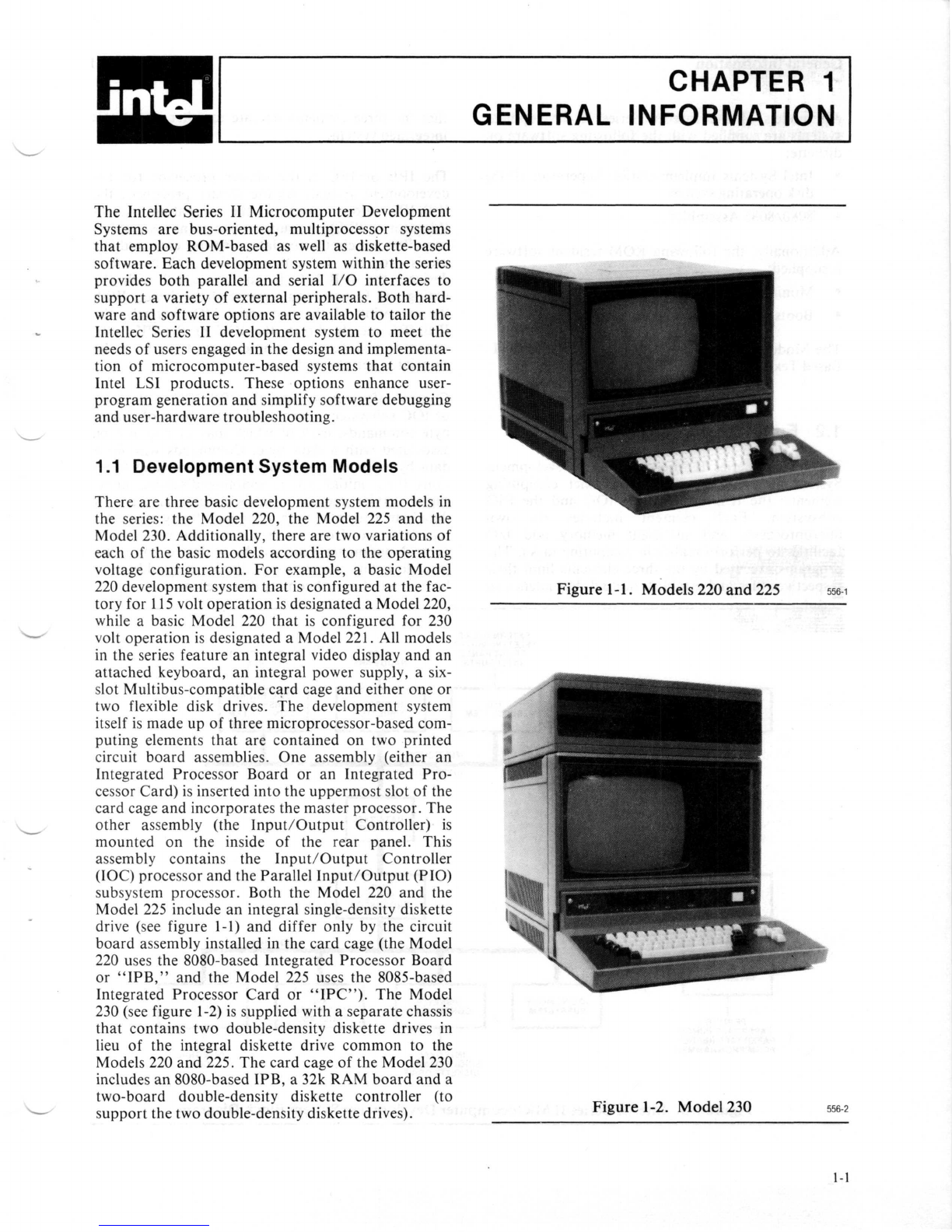
1.1
DevelopmentSystemModels
There
are
threebasicdevelopmentsystemmodels
in
the
series:
the
Model
220,
the
Model
225andthe
Model
230.
Additionally,there
aretwo
variations
of
each
ofthe
basic
models
according
tothe
operating
voltage
configuration.
For
example,
a
basicModel
220
developmentsystemthat
is
configured
atthe
fac-
tory
for
115
voltoperation
is
designated
a
Model220,
while
a
basicModel
220
that
is
configured
for230
volt
operation
is
designated
a
Model
221.
All
models
in
the
series
feature
an
integralvideodisplay
andan
attachedkeyboard,
an
integralpowersupply,
a
six-
slot
Multibus-compatiblecardcage
and
either
oneor
two
flexible
diskdrives.
The
developmentsystem
itself
is
made
upof
threemicroprocessor-basedcom-
puting
elementsthat
are
contained
ontwo
printed
circuit
board
assemblies.
One
assembly(either
an
Integrated
ProcessorBoard
oran
Integrated
Pro-
cessor
Card)
is
insertedinto
the
uppermostslot
ofthe
cardcage
and
incorporates
the
masterprocessor.
The
other
assembly
(the
Input/OutputController)
is
mounted
onthe
inside
ofthe
rearpanel.This
assembly
contains
the
Input/OutputController
(IOC)processor
andthe
ParallelInput/Output
(PIO)
subsystem
processor.Both
the
Model
220andthe
Model
225
include
an
integralsingle-densitydiskette
drive
(see
figure
1-1)
and
differ
only
bythe
circuit
boardassemblyinstalled
inthe
cardcage(theModel
220
uses
the
8080-based
Integrated
Processor
Board
or
"IPB,"
andthe
Model
225
uses
the
8085-based
Integrated
Processor
Card
or
"IPC").
The
Model
230
(see
figure
1-2)
is
supplied
with
a
separatechassis
thatcontains
two
double-densitydiskettedrives
in
lieu
ofthe
integraldiskettedrivecommon
tothe
Models
220and
225.
The
cardcage
ofthe
Model
230
includes
an
8080-based
IPB,
a 32kRAM
board
anda
two-boarddouble-densitydiskettecontroller
(to
support
thetwo
double-densitydiskettedrives).
Figure
1-1.
Models
220and225
556-1
Figure
1-2.
Model
230
556-2
1-1

General
Information
Intellec
Series
II
All
models
ofthe
IntellecSeries
II
development
systems
are
suppliedwith
the
followingsoftware
on
diskette:
•
IntelSystemsImplementationSupervisor(ISIS)
disk
operatingsystem
•
8080/8085
Assembler
Additionally,
the
followingROM-residentsoftware
is
supplied:
•
Monitorprogram
•
Bootstrap/Diagnosticprogram
The
Models
225and230
alsoincludeIntel'sCRT-
BasedTextEditor(CREDIT)
on
diskette.
that
the
threeelementsoperatetogether
asa
single
integratedsystem.
The
IPB
or
IPC
isthe
masterprocessor
forthe
developmentsystem.
Asthe
masterprocessor,
the
IPB/IPC
aloneexecutes
the
operatingsystem
(Monitor
or
ISIS),
the
supportprograms(assembler,
compilers,in-circuitemulatordrivers,etc.)
andthe
user'sprogram.
In
communicatingwithmost
I/O
devices,
the
IPB/IPC
isnot
concernedwith
the
timing
and
formatrequirements
ofthe
device.With
the
exception
ofthetwo
serial
I/O
channels,
the
IPB/IPC
merelydirects
theIOCorthe
PIO
sub-
system
to
transfer
oneor
morebytes
toor
from
the
associatedperipheraldevice.
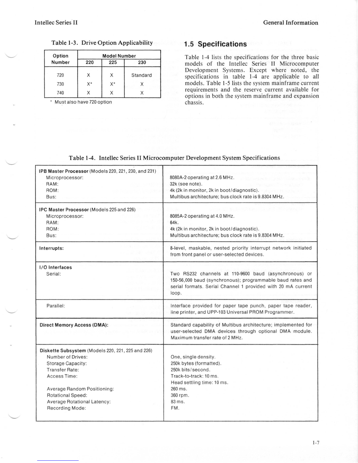
1.2
FunctionalOrganization
The
IntellecSeries
II
MicrocomputerDevelopment
System
is
made
upof
threedistinctcomputing
elements:
theIPBor
IPC,
theIOCandthePIO
subsystem.
Eachelementincludes
itsown
microprocessor
and
sufficient
memory
andI/O
facilities
to
performreal-timecomputingtasks.
The
programsexecuted
bythe
threeelementslimittheir
respective
roles
and
establishmutualdependence
so
Controlinformationfrom
the
IPB/IPC
tothePIO
orIOC
subsystem
is
provided
inthe
form
of
single-
byte
commands,each
of
which
mayormaynotbe
associatedwith
a
data
byte.Commandswithout
a
databyte
are
used
to
controloperations
and
func-
tions
(i.e.,initialization,enabling/disablinginter-
rupts,
servicerequestacknowledgementsetc.).
A
databyteassociatedwith
a
command
maybetheac-
tual
data
toor
from
the
device,
a
statusreturn,
ora
controlparameterrequired
bya
devicecontroller
prior
toa
data
transfer(e.g.,
the
startingaddress
or
byte
count
ofa
forthcomingdiskettetransfer).
.
I
PIO
SLAVE
PROCESSOR
1
PIO
BUS
PERIPHERAL
INTERFACE
EXTERNALCRT,
TELETYPEWRITER,
FRONT
PANEL
INTERRUPTSUSER
HARDWAREDOUBLE-DENSITY
DRIVES
MASTERMEMORY
PROCESSOR
SUBSYSTEM
I/O
SUBSYSTEM
32K
OR
64K
RAM
SUBSYSTEM
(IPB
OR
IPC)
4KROM
INCI
•
EMUL
1
1
MULTIBUS™
INTERFACE
PIO
DATA
BYTE
'
BUFFER
RCUIT
.ATOR
I
IOC
DATABYTE
BUFFER
TWO
BOARD
DISKETTE
CONTROLLER
(MODEL
230)
1
PRINTER
PAPERTAPE
PUNCH
PAPER
TAPE
READER
PROMPROGRAMMER
I
IOC
SLAVE
PROCESSOR
I
IOC
MEMORY
SUBSYSTEM
I
1
IOC
BUS
DISKETTE
CONTROLLER
1
KEYBOARD
AND
KEYBOARD
PROCESSOR
1
CRT
CONTROLLER
INTEGRAL
SINGLE-DENSITY
DISKETTEDRIVE
INTEGRAL
CRT
Figure
1-3.
Intellec
Series
II
Microcomputer
Development
System
Block
Diagram
556-3
_
^
1-2

IntellecSeries
II
General
Information
TheIOCand
PIO
subsystem
are
generallyinactive
except
whenresponding
toa
commandfrom
the
IPB/IPC.
Any
validcommandfrom
the
IPB/IPC
is
acceptedwithoutreservation(provided
any
previous
command
has
beencompleted)
andis
immediately
processed.Duringcommandexecution,both
the
IOCandPIO
subsystemrevisetheirrespectivedata
byte
buffer
(DBB)flags
to
indicateacceptance
ofthe
command,acceptance
ofany
associated
data
byte
or
the
completion
of
commandprocessing.
The
operatingsystem(Monitor
or
ISIS)polls
theDBB
flags
to
determine
the
status
of
commandexecution
by
theIOCorPIO
subsystem.Notethat
the
only
byte
returned
tothe
IPB/IPC
asa
statusbyte
isthe
DBB
flag
byte.
All
other
statusinformationfrom
the
IOCorthePIO
subsystem
is
returned
asa
databyte
that
is
recognized
as
statusonly
by
software.
The
same
is
true
for
commands;
the
onlytruecommand
is
a
directive
totheIOCorPIO
subsystem.Parameters
sent
to
devicecontrollers
are
output
as
data
bytes
and
are
recognized
as
parametersonly
bytheIOCorPIO
subsystem
software.
Few
interrupts
are
implemented
bythe
IntellecSeries
II
developmentsystemhardware;interruptsthat
are
implemented
are
normally
not
enabled
bythe
system
software
(Monitor
or
ISIS).
The
IPB/IPC
does,
however,
makegeneral
useof
servicerequeststhat
appear
as
bits
within
statusbytesreturnedfrom
the
IOC
orPIO
subsystem.
The
servicerequests
are
often
calledinterruptssincetheyinform
the
master
processorthat
a
taskinitiated
bya
command
has
beencompleted.However,
itis
important
to
remember
thatservicerequests
are
returnedwhen
the
master
processorpolls
theIOCorPIO
subsystem
to
determine
its
status;trueinterrupts
are
initiated
by
hardwarewithoutpolling.
It
isnot
necessary
forthe
masterprocessor
to
continually
poll
theIOCandPIOto
detect
the
occurrence
of
mosthardwareeventssincethese
events
are
generallyinitiated
by
commandsfrom
the
IPB/IPC.
In
otherwords,pollingaftereach
command
is
adequate
for
mostdevices.However
the
keyboard
oftheIOC(ora
keyboardassociatedwith
either
serial
I/O
channel)
isan
exception
in
that
key
entries
arenot
dependent
on
IPB/IPC
commands.
Anotherexception
isany
operator-controlleddevice
connected
tothe
PROMprogrammerconnector
of
the
PIO
subsystem.
The
master
processor
periodi-
cally
pollsboth
theIOCandthePIOto
accessstatus
bytescontainingservicerequests.
a
two-boarddiskettedrivecontroller
anda 32kRAM
board
are
alsoinsertedinto
the
cardcage.
The
backplane
board
ofthe
cardcage
is
designed
for
compatibilitywith
the
IntelMultibusarchitecture.
Thisarchitecture
is
represented
bya
collection
of86
lines
thatprovides
a
communicationspathamong
all
bus-compatible
boardsinstalled
inthe
cardcage.
All
Intel
singleboardcomputers
and
associatedmemory,
peripheral
devices
and
peripheraldevicecontrollers
adhere
tothe
Multibusarchitecture.
The
Multibusarchitecturepermits
any
master
processorinstalled
inthe
backplane
to
assume
full
control
ofthe
bus.
In
assumingcontrol
ofthe
bus,
each
bus
master
has
access
tothe
resources
ofany
other
bus
master.
In
terms
ofthe
IntellecSeries
II
development
system,another
bus
master
canadd
resources
and
featuresunavailable
inthe
standard
system.
In
terms
of
another
bus
master,
the
develop-
ment
system'sresources
are
available
tothebus
master
anddonot
have
tobe
duplicated.
The
available
developmentsystemresourcesinclude
allof
the
IPB/IPC
RAM,MonitorROM,
the
entire
IOC
with
its
subordinate
CRTand
integraldiskettedrive,
andthe
entire
PIO
subsystemwith
its
subordinate
papertapereader/punch,lineprinter
and
PROM
programmerperipherals.
Tousethe
resources
ofthe
development
system,
thebus
mastermust
usethe
memory
andI/O
port
addressesassigned
bythe
Intellec
Series
II
developmentsystem
as
described
in
this
manual.
Afew
facilities
ofthe
developmentsystemthat
are
implemented
on
both
theIPBandthe
IPC
are
inaccessible
to
another
bus
master.
Onthe
IPB,these
facilities
include
thebusand
systemcontrollers,
the
control
port
(portFF),
both
serial
I/O
channels,
the
interval
timer
and
bothinterruptcontrollers.
Onthe
IPC,only
thebus
controller,controlport
andthe
systm
interruptcontroller
are
inaccessible
to
another
bus
master.
Table
1-1
defines
the
Multibusinterface
pin
assignments,
and
table
1-2
describes
the
individual
signals.
1.3
Multibus
Architecture
As
previouslystated,either
anIPBorIPC
assembly
is
insertedinto
thetop
slot
ofthe
development
system's
cardcageand,
inthe
case
ofthe
Model230,
1.4
Options
Numerous
options
are
available
forthe
IntellecSeries
II
MicrocomputerDevelopmentSystems
to
expand
a
system'sresources
and
functions.Severaloptions
are
alsoavailable
to
"upgrade'
an
existingmodel
toa
modelwithincreasedresources.(For
a
completelist
of
availableoptions,refer
tothe
Intel
Systems
Data
Catalogue.)
1-3

General
Information
Intellec
Series
II
Table
1-1.
MultibusInterface
Pin
Assignments
Board
Component
Side
Pin
1
3
5
7
9
11
13
15
17
19
21
23
25
27
29
31
33
35
37
39
41
43
45
47
49
51
53
55
57
59
61
63
65
67
69
71
73
75
77
79
81
83
85
Mnemonic
GND
+
5
+5
+12
-5
GND
BCLK/
BPRN/
BUSY/
MRDC/
IORC/
XACK/
AACK/
BHEN/
CBRQ/**
CCLK/
INTA/*
INT6/
INT4/
INT2/
INTO/
ADRE/
ADRC/
ADRA/
ADR8/
ADR6/
ADR4/
ADR2/
ADRO/
DATE/
DATC/
DATA/
DAT8/
DAT6/
DAT4/
DAT2/
DATO/
GND
-10
-12
+
5
+
5
GND
Description
Signalground
+
5VDC
+
5VDC
+
12VDC
-5VDC
Signalground
Bus
Clock
Bus
Priority
In
Bus
Busy
MemoryReadCommand
I/O
ReadCommand
Transfer
Acknowledge
Advanced
Acknowledge
Byte
HighEnable
Common
Bus
Request
ConstantClock
InterruptAcknowledge
InterruptRequests
Address
Lines
•
.
Data
Lines
Signalground
-10VDC
-12VDC
+
5VDC
+
5VDC
Signalground
Board
Circuit
Side
Pin
2
4
6
8
10
12
14
16
18
20
22
24
26
28
30
32
34
36
38
40
42
44
46
48
50
52
54
56
58
60
62
64
66
68
70
72
74
76
78
80
82
84
86
Mnemonic
GND
+
5
+5
4-12
-5
GND
INIT/
BPRO/*
BREQ/
MWTC/
IOWC/
INH1/
INH2/
ADR10/
ADR11/
ADR12/
ADR13/
INT7/
INT5/
INT3/
INT1/
ADRF/
ADRD/
ADRB/
ADR9/
ADR7/
ADR5/
ADR3/
ADR1/
DATF/
DATD/
DATB/
DAT9/
DAT7/
DAT5/
DAT3/
DAT1/
GND
-10
-12
+
5
+5
GND
Description
Signalground
+
5VDC
+
5VDC
+
12VDC
-5VDC
Signalground
Initialize
Bus
Priority
Out
Bus
Request
MemoryWriteCommand
I/O
WriteCommand
Inhibit
(disable)
RAM
Inhibit
(disable)
ROM
Address
Extension
Lines
InterruptRequests
AddressLines
DataLines
Signalground
-10VDC
-12VDC
+
5VDC
+
5VDC
Signalground
*
Not
implemented
on
IPB/IPC
**
Onlyimplemented
on
IPC
•
1-4

IntellecSeries
II
GeneralInformation
Table1-2.Multibus
Interface
SignalDescriptions
Signal
Mnemonic
Functional
Description
AACK/
ADRO/-ADRF/
ADR10/-ADR13/
BCLK/
BHEN/
BPRN/
BPRO/
BREQ/
BUSY/
CBRQ/
CCLK/
DATO/-DATF/
INH1/
INH2/
INIT/
Advanced
Acknowledge.
A
memoryacknowledge
signal
that
is
generated
in
advance
ofthe
normaltransferacknowledge
(XACK/)
signal
to
allow
a bus
master
to
shorten
its
memoryaccess
timing.
Address.
These
16
lines
are
used
to
specify
the
address
ofthe
memorylocation
or
I/O
port
tobe
accesedwithin
a 64k
range.
ADRF/
isthe
leastsignificantbit.
Extended
Address.
Thesefourlines
are
appended
tothe
16-bitaddress
to
increase
the
addressingrange
to1
megabyte.
The
IPB/IPC
monitorstheseinputs
to
deter-
mine
ifthe
address
onthebus
corresponds
toits
memorysegment
(0-64k).
ADR10/
isthe
leastsignificant
bitofthe
extendedaddress.
Bus
Clock.
An
asynchronousclocksignalused
to
synchronize
bus
contention
resolvingcircuitsamong
bus
masters.
The
BLCK/signalfrom
the
IPB/IPC
hasa
minimumperiod
of100ns
with
a
35%-65%
(minimum)dutycycle.
Byte
High Enable.
A
signalthatindicates
the
presence
ofa
databyte
onthe
DAT8/-DATF/
datalines.Thissignal
is
supportedonly
bythe
memory
onthe
IPC.
Bus
Priority
In.A bus
contention
resolving
signal
that
indicates
toa bus
masterthat
no
higher-priority
bus
master
is
requesting
the
bus.
The
IPB/IPCincorporates
the
bus
resolutionlogic
and
provides
an
individual
BPRN/
signal
to
eachcard-cage
slot.
BPRN/
is
synchronized
by
BCLK/.
Bus
Priority Out.
A bus
contentionresolvingsignal
foruse
withserial(daisychain)
bus
priorityresolutionschemes
(BPRO/
is
passed
tothe
BPRN/
input
ofthe
next
lower-priority
bus
master).
BPRO/
isnot
supported
bythe
IPB/IPC.
Bus
Request.
A bus
contentionresolvingsignal
foruse
withparallel-priority
resolutionschemes.
A bus
masteruses
BREQ/
to
indicatethat
it
requires
the
bus.
The
IPB/IPCmonitors
the
individual
BREQ/
inputs
and
outputs
BPRN/
tothe
highest-priority
bus
masterrequesting
the
bus.
BREQ
is
synchronized
by
BCLK/.
Bus
Busy.
A
common
bus
contentionresolvingsignal
to
indicatesthat
thebusisin
use.When
a bus
mastergainsaccess
the
bus,
it
uses
BUSY/
to
prevent
any
other
bus
masterfromacquiring
the
bus.
BUSY/
is
synchronized
by
BCLK/.
Common
Bus
Request.
A bus
contentionresolvingsignal
to
allow
bus
requests
by
lower-priority
bus
masters
to
override
bus
requests
by
high-priority
bus
masters.
CBRQ/
is
synchronized
by
BCLK/
andis
supportedonly
bythe
IPC.
Constant Clock.
An
asynchronousclocksignalavailable
for
general
useby
modules
onthe
bus.
Onthe
IPB/IPC,
CCLK/
is
synchronouswith
BCLK/
andhasthe
same
period
and
dutycycle.
Data.
These
16
bidirectionallinestransferdata
toor
from
the
addressedmemory
location
orI/O
port.
DATO/
isthe
least-significantbit.
The
IPB/IPC,
asa bus
master,
has
a
8-bitwidedatapath
and
onlyuses
DATO/-DAT7/.
TheIPC
memory
canuseall
16
data
lines
(DATO/-DATF/).
Inhibit
RAM. Prevents
RAM
devicesfromresponding
tothe
memoryaddress
onthe
address
lines.
INH1
/
effectivelyallows
ROM
devices
to
override
RAM
deviceswhen
ROM
andRAMare
assigned
the
sameaddressspace.
INH1/
may
also
be
used
to
allow
memorymapped
I/O
devices
to
overrideRAM.
Inhibit
ROM. Prevents
ROM
devicesfromresponding
tothe
memoryaddress
onthe
addresslines.
INH2/
effectively
allowsstart-up
software
such
as
ROM-based
bootstrapprograms
to
overrideanother
ROM
devicewhen
thetwo
ROMs
are
assigned
the
sameaddressspace.
INH2/
may
also
be
used
to
allowmemory
mapped
I/O
devices
to
overrideROM.
Initialize.
Thissignalresets
the
entiresystem
toa
knowninternalstate.
INIT/
is
activated
bythe
frontpanel
RESET
switch.Whenactivated
by
another
bus
master,
INIT/
will
not
initialize
the
IPB/IPC.
1-5

General
InformationIntellec
Series
II
Table
1-2.
Multibus
Interface
SignalDescriptions
(Cont'd.)
Signal
Mnemonic
Functional
Description
INTO/-INT7/
INTA/
Interrupt.
A setof
eight,multilevelinterruptrequestlinesaccepted
bythe
parallel
interruptresolvinglogic
ofthe
IPB/IPC
(INTO/
isthe
highest-
priorityinterrupt).
In
response
toan
interrupt,
the
IPB/IPCexecutes
an
interruptacknowledgesequence
to
call
the
associateduserinterrupt
service
routine.
Interrupt
Acknowledge.
A
signalgenerated
bya
masterprocessor
in
response
toan
interrupt.Since
the
IPB/IPCincorporates
the
interrupt
resolutionlogic,
the
INTA/
signal
is
usedinternally
andisnot
output
on
the
bus.
IORC/
IOWC/
MRDC/
I/O
Read
Command.
Thissignalindicatesthat
the
address
of
port
has
beenplaced
onthe
addresslines
and
that
the
port
isto
requesteddatabyte
onthe
datalines.
an
input
place
the
MWTC/
XACK/
I/O
Write
Command.
Thissignalindicatesthat
the
address
ofan
output
port
has
beenplaced
onthe
addresslines
and
that
the
databyte
onthe
data
lines
istobe
accepted
bythe
port.
Memory
Read
Command.
Indicatesthat
the
address
ofa
memorylocation
has
been
placed
onthe
addresslines
and
that
the
requesteddatabyte
isto
be
placed
onthe
datalines.
Memory
Write
Command.
Indicatesthat
the
address
ofa
memory
location
has
beenplaced
onthe
addresslines
and
that
the
databyte
tobe
written
into
the
addressedlocation
has
beenplaced
onthe
datalines.
Transfer
Acknowledge.
Thissignal
is
the
responsefrommemory
oran
I/O
portthatindicatesthat
the
specifiedread/writeoperation
has
been
completed.That
is,
data
has
beenplaced
on,or
acceptedfrom,
the
data
lines.
_
1.4.1Expansion
Chassis
A
four-slot
expansionchassis
is
available
to
increase
the
cardcagecapacity
ofany
model
from
six
slots
to
ten
slots.
The
expansionchassis
is
mountedbelow
the
system
chassis
and
includes
the
required
bus
interface
cables
anditsown
internal
powersupply.
1.4.2
Universal
PROM
Programmer
The
Intel
Universal
PROMProgrammer
(UPP-103)
allows
a
user
to
program
and
verify
anyofthe
standard
Intel
PROMs
and
EPROMs.
The
PROM
programme^
interfaces
directly
tothe
UPP
connector
onthe
rearpanel
ofthe
systemchassis
and
includes
the
required
interface
cable
anditsown
internal
power
supply.
The
PROMprogrammer
is
supplied
with
two,user-selectedpersonalitymodules
anda
diskette
thatcontains
the
Universal
PROMMapper
(UPM)
controlprogram.
1.4.3
In-Circuit
Emulators
A
number
of
in-circuit
emulators
and
microcomputer
development
systemssupportpackages
are
available
to
support
Intel
microcomputer
and
microprocessor
family
devices.
In-circuit
emulators
simplify
hard-
ware
troubleshooting
and
program
debugging
ina
user's
system
by
emulating
the
system'smicro-
computer
or
microprocessor
in
realtime.
In-circuit
emulators
are
available
forthe
MCS-48
family
microcomputers
andthe
8080,8085
and
8086
family
microprocessors.
1.4.4
High-Level
Languages
Several
high-levellanguages
are
available
(on
diskette)
forthe
IntellecSeries
II
development
systems
including
a
PL/Mcompiler,
a
FORTRAN
compiler,
PASCALcompiler
anda
BASIC
interpreter.
1.4.5
IPC
Upgrade
Kit
TheIPC
upgrade
kit
replaces
the
8080-based
IPB
assembly
ina
Model
220or
Model
230
with
an
8085-
based
IPC
assembly
as
supplied
with
the
Model225.
1.4.6DiskDrives
Three
disk
drive
options
are
available
to
increase
the
on-line
storagecapacity
ofany
development
system.
A
complete
double-density
diskette
drive
system
as
well
asa
dual
double-density
drive
chassis
are
available.
Both
of
theseoptions
add1
megabyte
of
on-line
storage
toan
existing
system.
The720
Option
consists
ofa
two-board
flexible
disk
drive
controller
set
anda
dual
drive
chassis,
while
the730
Option
includes
only
the
dual
drive
chassis.
The
Option
740
is
a
complete
hard-disk
subsystem
(two-boardhard
disk
drive
controller
setand
drive)
thatprovides
an
additional
7.3
megabytes
of
storage.Table
1-3
defines
the
drive
option
applicability
forthe
three
development
systemmodels.
_
_
_
1-6
IntellecSeries
II
GeneralInformation
Table
1-3.Drive
Option
Applicability
Option
Number
720
730
740
Model
Number
220
X
X*
X
225
X
X*
X
230
Standard
X
X
*
Must
alsohave
720
option
1.5
Specifications
Table
1-4
lists
the
specifications
forthe
three
basic
models
ofthe
Intellec
Series
II
Microcomputer
Development
Systems.
Except
where
noted,
the
specifications
in
table
1-4are
applicable
toall
models.
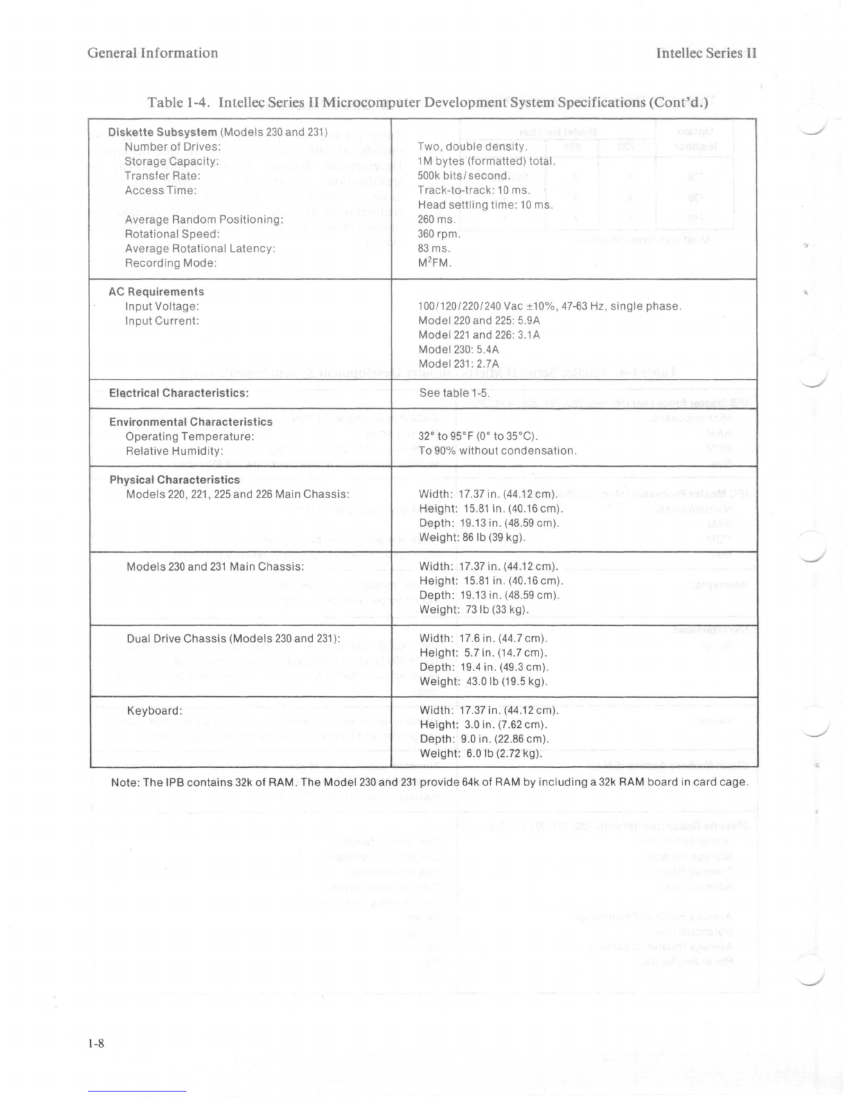
Table
1-5
lists
the
system
mainframe
current
requirements
andthe
reserve
current
available
for
options
in
both
the
system
mainframe
and
expansion
chassis.
Table
1-4.
IntellecSeries
II
MicrocomputerDevelopmentSystemSpecifications
IPB
Master
Processor(Models220,
221,
230,
and
231)
Microprocessor:
RAM:
ROM:
Bus:
8080A-2
operating
at2.6
MHz.
32k
(seenote).
4k
(2kin
monitor,
2kin
boot/diagnostic).
Multibusarchitecture;
bus
clockrate
is
9.8304
MHz,
IPC
Master
Processor(Models
225and
226)
Microprocessor:
RAM:
ROM:
Bus:
8085A-2
operating
at4.0
MHz.
64k.
4k
(2kin
monitor,
2kin
boot/diagnostic).
Multibusarchitecture;
bus
clockrate
is
9.8304
MHz.
Interrupts:
8-level,
maskable,nestedpriorityinterruptnetworkinitiated
from
frontpanel
or
user-selecteddevices.
I/O
Interfaces
Serial:
Two
RS232
channels
at
110-9600
baud(asynchronous)
or
150-56,000
baud(synchronous);programmablebaudrates
and
serialformats.SerialChannel
1
providedwith
20
mA
current
loop.
Parallel:
Interfaceprovided
for
papertapepunch,papertapereader,
line
printer,
and
UPP-103
UniversalPROMProgrammer.
Direct
Memory
Access
(DMA):
Standardcapability
of
Multibusarchitecture;implemented
for
user-selected
DMA
devicesthroughoptional
DMA
module.
Maximum
transferrate
of2
MHz.
Diskette
Subsystem(Models220,
221,
225and
226)
Number
of
Drives:
StorageCapacity:
Transfer
Rate:
Access
Time:
Average
Random
Positioning:
Rotational
Speed:
Average
Rotational
Latency:
Recording
Mode:
One,singledensity.
250k
bytes(formatted).
250k
bits/second.
Track-to-track:
10
ms.
Headsettlingtime:
10ms.
260ms.
360
rpm.
83ms.
FM.
1-7
GeneralInformation
Intellec
Series
II
Table1-4.IntellecSeries
II
MicrocomputerDevelopmentSystemSpecifications(Cont'd.)
DisketteSubsystem(Models
230and
231)
Number
of
Drives:
StorageCapacity:
Transfer
Rate:
Access
Time:
Average
RandomPositioning:
RotationalSpeed:
Average
RotationalLatency:
RecordingMode:
AC
Requirements
InputVoltage:
InputCurrent:
Electrical
Characteristics:
Environmental
Characteristics
OperatingTemperature:
Relative
Humidity:
Physical
Characteristics
Models220,
221,
225and226
MainChassis:
Models
230and231
MainChassis:
Dual
DriveChassis(Models
230and
231):
Keyboard:
Two,
doubledensity.
1M
bytes(formatted)
total.
500k
bits/second.
Track-to-track:
10ms.
Headsettlingtime:
10ms.
260ms.
360
rpm.
83ms.
M2FM.
100/120/220/240
Vac
±10%,47-63
Hz,
single
phase.
Model
220
and
225:
5.9A
Model
221
and
226:
3.1
A
Model
230:5.4A
Model
231:
2.7A
See
table1-5.
32°to950F(0°to350C).
To
90%
without
condensation
Width:
17.37
in.
(44.12
cm).
Height:
15.81
in.
(40.16cm).
Depth:
19.13
in.
(48.59
cm).
Weight:
86
Ib
(39
kg).
Width:
17.37
in.
(44.12
cm).
Height:
15.81
in.
(40.16cm),
Depth:
19.13
in.
(48.59
cm).
Weight:
73
Ib
(33
kg).
Width:
17.6
in.
(44.7
cm).
Height:
5.7in.
(14.7cm).
Depth:
19.4
in.
(49.3cm).
Weight:43.0
Ib
(19.5kg).
Width:17.37
in.
(44.12
cm).
Height:
3.0
in.
(7.62cm).
Depth:
9.0in.
(22.86cm).
Weight:
6.0Ib
(2.72
kg).
_
Note:
The
IPB
contains
32kof
RAM.
The
Model
230and231
provide
64kofRAMby
including
a 32kRAM
board
in
cardcage.
_
1-8
IntellecSeries
II
GeneralInformation
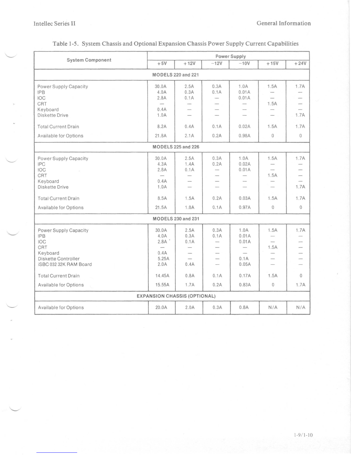
Table
1-5.
SystemChassis
and
OptionalExpansionChassisPowerSupplyCurrentCapabilities
System
Component
Power
Supply
+5V
+12V
-12V-10V
-I-
15V
+
24V
MODELS
220and221
PowerSupplyCapacity
IPB
IOC
CRT
Keyboard
Diskette
Drive
TotalCurrentDrain
Available
for
Options
30.0A
4.0A
2.8A
—
0.4A
1.0A
8.2A
21
.8A
2.5A
0.3A
0.1A
—
—
—
0.4A
2.1A
0.3A
0.1A
—
—
—
—
0.1A
0.2A
1.0A
0.01A
0.01A
—
—
—
0.02A
0.98A
1.5A
—
—
1.5A
—
—
1.5A
0
1.7A
—
—
—
—
1.7A
1.7A
0
MODELS
225and226
PowerSupplyCapacity
IPC
IOC
CRT
Keyboard
DisketteDrive
TotalCurrentDrain
Available
for
Options
30.0A
4.3A
2.8A
—
0.4A
1.0A
8.5A
21.
5A
2.5A
1.4A
0.1A
—
—
—
1.5A
1.0A
0.3A
0.2A
—
—
—
—
0.2A
0.1A
1.0A
0.02A
0.01A
—
—
—
0.03A
0.97A
1.5A
—
—
1.5A
—
—
1.5A
0
1.7A
—
—
—
—
1.7A
1.7A
0
MODELS
230and231
Power
SupplyCapacity
IPB
IOC
CRT
Keyboard
DisketteController
iSBC
03232KRAM
Board
TotalCurrentDrain
Available
for
Options
30.0A
4.0A
2.8A
'
—
0.4A
5.25A
2.0A
14.45A
15.55A
2.5A
0.3A
0.1A
—
—
—
0.4A
0.8A
1.7A
0.3A
0.1A
—
—
—
—
—
0.1A
0.2A
1.0A
0.01A
0.01A
—
—
0.1A
0.05A
0.17A
0.83A
1.5A
—
—
1.5A
—
—
—
1.5A
0
1.7A
—
—
—
—
—
—
0
1.7A
EXPANSION
CHASSIS(OPTIONAL)
Available
for
Options
20.
OA
2.0A0.3A0.8A
N/A
N/A
1-9/1-10

-
_
-
CHAPTER
2
INTEGRATED
PROCESSOR
BOARD
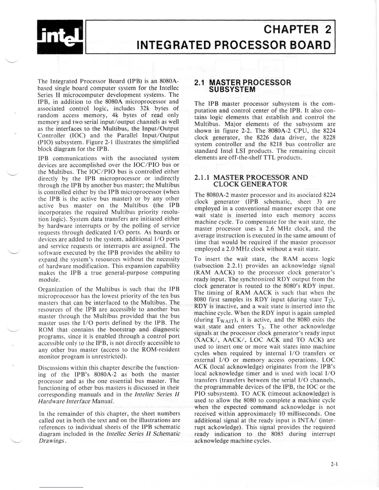
The
Integrated
Processor
Board
(IPB)
isan
8080A-
basedsingle
board
computersystem
forthe
Intellec
Series
II
microcomputerdevelopmentsystems.
The
IPB,
in
addition
tothe
8080A
microprocessor
and
associatedcontrollogic,includes
32k
bytes
of
randomaccessmemory,
4k
bytes
of
readonly
memory
andtwo
serialinput/outputchannels
as
well
asthe
interfaces
tothe
Multibus,
the
Input/Output
Controller(IOC)
andthe
ParallelInput/Output
(PIO)
subsystem.Figure
2-1
illustrates
the
simplified
blockdiagram
forthe
IPB.
IPB
communicationswith
the
associatedsystem
devices
are
accomplishedover
the
IOC/PIO
busor
the
Multibus.
The
IOC/PIO
busis
controlledeither
directly
bytheIPB
microprocessor
or
indirectly
through
theIPBby
another
bus
master;
the
Multibus
is
controlledeither
bytheIPB
microprocessor(when
the
IPBisthe
active
bus
master)
orbyany
other
active
bus
master
onthe
Multibus(the
IPB
incorporates
the
requiredMultibuspriorityresolu-
tionlogic).System
data
transfers
are
initiatedeither
by
hardwareinterrupts
orbythe
polling
of
service
requeststhroughdedicated
I/O
ports.
As
boards
or
devices
are
added
tothe
system,additional
I/O
ports
and
servicerequests
or
interrupts
are
assigned.
The
software
executed
bytheIPB
provides
the
ability
to
expand
the
system'sresourceswithout
the
necessity
of
hardwaremodification.Thisexpansioncapability
makes
theIPBa
truegeneral-purposecomputing
module.
Organization
ofthe
Multibus
is
suchthat
theIPB
microprocessor
hasthe
lowestpriority
ofthetenbus
mastersthat
canbe
interfaced
tothe
Multibus.
The
resources
oftheIPBare
accessible
to
another
bus
masterthrough
the
Multibusprovidedthat
thebus
masteruses
theI/O
ports
defined
bythe
IPB.
The
ROM
thatcontains
the
bootstrap
and
diagnostic
programs,since
itis
enabledthrough
a
controlport
accessibleonly
tothe
IPB,
isnot
directlyaccessible
to
any
other
bus
master(access
tothe
ROM-resident
monitorprogram
is
unrestricted).
2.1
MASTER
PROCESSOR
SUBSYSTEM
Discussions
within
thischapterdescribe
the
function-
ing
ofthe
IPB's
8080A-2
as
both
the
master
processor
andastheone
essential
bus
master.
The
functioning
of
other
bus
masters
is
discussed
in
their
correspondingmanuals
andinthe
Intellec
Series
II
Hardware Interface
Manual.
In
the
remainder
of
thischapter,
the
sheetnumbers
called
outin
both
the
text
andonthe
illustrations
are
references
to
individualsheets
oftheIPB
schematic
diagramincluded
inthe
Intellec
Series
II
Schematic
Drawings.
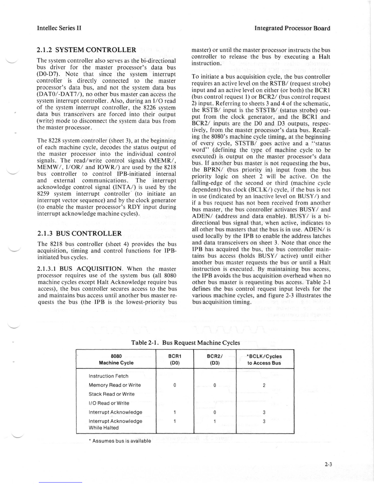
TheIPB
master
processor
subsystem
isthe
com-
putation
and
controlcenter
ofthe
IPB.
It
alsocon-
tainslogicelementsthatestablish
and
control
the
Multibus.
Majorelements
ofthe
subsystem
are
shown
in
figure
2-2.
The
8080A-2
CPU,
the
8224
clock
generator,
the
8226
data
driver,
the
8228
system
controller
andthe
8218
bus
controller
are
standardIntel
LSI
products.
The
remainingcircuit
elements
are
off-the-shelf
TTL
products.
2.1.1
MASTER
PROCESSOR
AND
CLOCK
GENERATOR
The
8080A-2masterprocessor
andits
asociated8224
clock
generator(IPBschematic,sheet
3)are
employed
ina
conventionalmannerexceptthat
one
wait
state
is
insertedintoeachmemoryaccess
machine
cycle.
To
compensate
forthe
waitstate,
the
master
processor
uses
a 2.6MHz
clock,
andthe
averageinstruction
is
executed
inthe
sameamount
of
timethatwould
be
required
ifthe
masterprocessor
employed
a 2.0MHz
clockwithout
a
waitstate.
To
insert
the
waitstate,
theRAM
accesslogic
(subsection2.2.1)provides
an
acknowledgesignal
(RAM
AACK)
tothe
processorclockgenerator's
readyinput.
The
synchronized
RDY
outputfrom
the
clock
generator
is
routed
tothe
8080's
RDY
input.
The
timing
ofRAM
AACK
is
suchthatwhen
the
8080
first
samples
itsRDY
input(duringstateT2),
RDY
is
inactive,
anda
waitstate
is
insertedinto
the
machine
cycle.When
theRDY
input
is
againsampled
(during
TWAIT)»
itis
active,
andthe
8080exits
the
wait
state
and
enters
T3.The
otheracknowledge
signals
atthe
processorclockgenerator'sready
input
(XACK/,
AACK/,
LOCACKandTO
ACK)
are
used
to
insert
oneor
morewaitstatesintomachine
cycles
whenrequired
by
internal
I/O
transfers
or
external
I/Oor
memoryaccessoperations.
LOC
ACK
(localacknowledge)originates
from
the
IPB's
localacknowledgetimer
andis
used
with
local
I/O
transfers
(transfersbetween
the
serial
I/O
channels,
the
programmabledevices
ofthe
IPB,
theIOCorthe
PIO
subsystem).
TOACK
(timeoutacknowledge)
is
used
to
allow
the
8080
to
complete
a
machinecycle
when
the
expectedcommandacknowledge
isnot
receivedwithinapproximately
10
milliseconds.
One
additionalsignal
atthe
readyinput
is
INTA/
(inter-
ruptackowledge).Thissignalprovides
the
required
readyindication
tothe
8085duringinterrupt
acknowledge
machinecycles.
2-1

Integrated
ProcessorBoard
Intellec
Series
II
RAMACK
SYS
CLOCK
GENERATORBCLK
MULTIBUS1"
XACK
CPU
CLOCK
GENERATOR
CLK
TOACK
LOCACK
BUS
CONTROLLER
MEM
RD/WRTCONTROL
MRDC.MWTC
I/O
RD/WRTCONTROL
IORC.IOWC
AOORESS/DATA
ENABLE
ADEN
READY
MASTER
PROCESSOR
DO-7
DBIN
WR
SYSTEM
BUS
CONTROL
AO-15
SYSTEM
CONTROLLER
DO-7
LOCACK
INTA
INTERRUPT
MULTIBUS
INTERRUPT
SWITCHES
INTERRUPTREQ
INT
DEBOUNCE
INTERRUPTS
INTERRUPT
CONTROLLERS
PIO
&
IOC
IPIO.ICRT
DATA/CMD/STAT
REALTIME
CLK
INT
RTC
CMD/STAT
ENABLE
SELI1.2
DATAREADY
INT
CMD/STAT
BUS
DRIVERS
RAM
ACCESS
REFRESH
CONTROL
RAM
S
SELCPU
LOCALACK
TIMER
"SEL
LOCAL
I/O
I/O
PORT
ADDRESS
DECODER
ENABLE
SELWR
ROMENB
SELCPU
SELPIO
SELCRT
ENABLE
EXTERNAL
LINE
DRIVERS
ROM
ACCESS
CONTROL
BOOT/
DIAGNOSTIC
ROM
MONITOR
ROM
DATO-7
DATA
LINES
CMD/STAT
RTC
BAUD
RATE
AND
REALTIME
COUNTERS
CHANO
EXTCLK
CHAN
1
EXTCLK
CURRENT
LOOP
DRIVERS
CHANO
DATA
SERIAL
I/O
CHANNEL
CON-
TROLLERS
CHANO-
CONTROL
CHAN
1
DATA
&
CONTROL
Figure
2-1.
IPB
Simplified
Block
Diagram
SERIAL
I/O
CHANNELS
556-4
RESET
SWITCH
RESET
READY
AACK
XACK
RAMACK
TOACK
LOG
ACK
INTA
BUS
OTHER
REQUEST
BUS
MASTERS
BREO19
23
4 MHz
XTAL
HDh
8224
PROCESSOR
CLOCK
GENERATOR
iNir
SYSTEM
INITIALIZE
RESET
PROCESSOR
CLOCK
2.6MHz
01.02
READY
ROY
STSTB
74148
74138
BUS
PRIORITY
RESOLUTION
LOGIC
SYNC
I/O
SUB-
SYSTEM
INT
ADDRESS
AO
15
ADDRESS
8080A
2
MASTER
PROCESSOR
BUSCONTROL
REQUEST
BCR1
(DO
BCR2(D3
CPU
BUS
CONTROL
DBIN
WR
8228
SYSTEM
CONTROLLER
3
^
DAI
^^0^
INTERRUPT
ACK
INTA
j
SYS
BUS
CONTROL
MEMR
MEMW
I/O
SUB
SYSTEM
ADDRESS
DRIVER
3
t
k
1
T
8226
DATA
DRIVER
3
t
1
BUSCONNECT
TRANSFER
START
REQUEST
I/OW
XSTR
REQUEST
STROBE
RSTB
BPRNO
8218
BUS
CONTROLLER
MRDC
MWTC
IORC
IOWC
BUSY
BUS
COMMANDS
10ms
BUS
TIMEOUT
2
XFER
NOT
COMPLETE
TOACK
MEMORY
SUBSYSTEM'
START
UPAND
RESET
BUS
ACCESS
OVERRIDE
OVRD
BUS
MASTER
SELECT
BRPN18
NOTE:
The
number
inthe
lower
right-hand
corner
of
each
block
identifies
the
sheet
number
oftheIPB
schematic.
Figure
2-2.MasterProcessorSubsystem
Block
Diagram
•
SYSTEM
INTERRUPT
CONTROLLER
556-5
_
-
2-2
Intellec
Series
II
Integrated
Processor
Board
2.1.2
SYSTEM
CONTROLLER
The
systemcontrolleralsoserves
asthe
bi-directional
bus
driver
forthe
master
processor's
data
bus
(DO-D7).
Note
that
since
the
systeminterrupt
controller
is
directlyconnected
tothe
master
processor's
data
bus,
andnotthe
systemdata
bus
(DATO/-DAT7/),
no
other
bus
master
can
access
the
systeminterruptcontroller.Also,during
anI/O
read
of
the
systeminterruptcontroller,
the
8226system
data
bus
transceivers
are
forcedintotheiroutput
(write)
mode
to
disconnect
the
system
data
bus
from
the
master
processor.
The
8228systemcontroller(sheet
3),atthe
beginning
of
eachmachinecycle,decodes
the
statusoutput
of
the
master
processor
into
the
individualcontrol
signals.
The
read/write
controlsignals(MEMR/,
MEMW/,
I/OR/
and
IOWR/)
are
used
bythe
8218
bus
controller
to
control
IPB-initiated
internal
and
externalcommunications.
The
interrupt
acknowledgecontrolsignal
(INTA/)
is
used
bythe
8259systeminterrupt
controller
(to
initiate
an
interrupt
vectorsequence)
andbythe
clockgenerator
(to
enable
the
master
processor's
RDY
inputduring
interruptacknowledgemachinecycles).
2.1.3
BUS
CONTROLLER
The
8218
bus
controller(sheet
4)
provides
thebus
acquisition,timing
and
controlfunctions
for
IPB-
initiated
bus
cycles.
2.1.3.1
BUS
ACQUISITION.
When
the
master
processorrequires
useofthe
system
bus
(all
8080
machinecyclesexcept
Halt
Acknowledgerequire
bus
access),
thebus
controllersecuresaccess
tothebus
and
maintains
bus
accessuntilanother
bus
master
re-
quests
thebus
(the
IPB
isthe
lowest-priority
bus
master)
or
until
the
masterprocessorinstructs
thebus
controller
to
release
thebusby
executing
a
Halt
••
instruction.
To
initiate
a bus
acquisitioncycle,
thebus
controller
requires
an
activelevel
onthe
RSTB/
(requeststrobe)
input
andan
activelevel
on
either
(or
both)
the
BCR1
(bus
controlrequest
1)or
BCR2/
(buscontrolrequest
2)
input.
Referring
to
sheets
3 and4 ofthe
schematic,
the
RSTB/
input
isthe
STSTB/
(statusstrobe)out-
put
from
the
clock
generator,
andthe
BCR1
and
BCR2/
inputs
aretheDOandD3
outputs,respec-
tively,
from
the
masterprocessor'sdatabus.Recall-
ing
the
8080's
machinecycletiming,
atthe
beginning
of
everycycle,
STSTB/
goes
active
anda
''status
word"
(defining
the
type
of
machinecycle
tobe
executed)
is
output
onthe
masterprocessor'sdata
bus.
If
another
bus
master
isnot
requesting
the
bus,
the
BPRN/(buspriority
in)
inputfrom
thebus
priority
logic
on
sheet
2
will
be
active.
Onthe
falling-edge
ofthe
second
or
third(machinecycle
dependent)
bus
clock(BCLK/)cycle,
ifthebusisnot
in
use
(indicated
byan
inactivelevel
on
BUSY/)
and
if
a bus
request
hasnot
beenreceived
from
another
bus
master,
thebus
controlleractivates
BUSY/
and
ADEN/
(address
and
data
enable).
BUSY/
isa bi-
directional
bus
signalthat,whenactive,indicates
to
all
other
bus
mastersthat
thebusisin
use.
ADEN/
is
used
locally
bytheIPBto
enable
the
addresslatches
and
data
transceivers
on
sheet
3.
Notethatonce
the
IPB
has
acquired
the
bus,
thebus
controllermain-
tains
bus
access(holds
BUSY/
active)
until
either
another
bus
masterrequests
thebusor
until
a
Halt
instruction
is
executed.
By
maintaining
bus
access,
the
IPB
avoids
thebus
acquisitionoverheadwhen
no
other
bus
master
is
requesting
bus
access.
Table
2-1
defines
thebus
controlrequestinput
levels
forthe
various
machinecycles,
and
figure
2-3
illustrates
the
bus
acquisitiontiming.
Table
2-1.
Bus
Request
Machine
Cycles
8080
Machine
Cycle
BCR1
(DO)
BCR2/
(D3)
*BCLK/Cycles
to
Access
Bus
Instruction
Fetch
Memory
Read
or
Write
Stack
Read
or
Write
I/O
Read
or
Write
Interrupt
Acknowledge
Interrupt
Acknowledge
While
Halted
1
1
3
3
*
Assumes
busis
available
2-3

Integrated
Processor
Board
Intellec
Series
II
If
thebusisinuse(if
BUSY/
is
low)
orifa bus
request
is
pending
(if
BPRN/
is
high),
thebus
controllerdelays
the
generation
of
BUSY/
and
ADEN/
until
one
BCLK/cycle
after
both
thebus
becomesavailable
andno
requests
are
pending.
2.1.3.2
BUS
RELEASE.
Once
the
masterpro-
cessor
has
acquired
the
bus,
it
surrenders
thebus
only
when
another
bus
masterrequests
thebusor
when
the
masterprocessorexecutes
a
HaltAcknowledge
machinecycle.Whenanother
bus
masterrequests
the
bus,
thebus
controllercompletes
its
current
bus
controlcycle
and
releases
thebus
(inactivates
BUSY/)
onthe
next
bus
clockcycle.When
a
Halt
Acknowledgemachinecycle
is
executed,
thebus
con-
troller
releases
thebusonthe
third
bus
clockcycle.
2.1.3.3
BUS
OVERRIDE.
Thebus
controller
has
an
OVRD(override)inputthat,whenactive,allows
the
masterprocessor
to
maintain
bus
accessbetween
bus
cycles
by
preventing
the
recognition
ofa bus
requestfromanother
bus
master.
The
OVRDinput
is
taken
from
bit6 oftheROM
enablelatch
andisset
or
resetthrough
the
IPB's
control
port.
Referring
to
the
schematic,OVRD
is
automaticallyactivated
when
the
system
is
initialized
to
prevent
any
other
bus
master
from
accessing
thebus
during
the
master
processor'sinitialization/start-upprocedure
(follow-
ing
initialization,
the
Monitorprograminactivates
OVRD).Duringsystemoperations,when
the
master
processormustmaintain
bus
access
fora
criticalcode
section(e.g.,whenperforming
a
test
andset
opera-
tion),
the
programwould
first
activateOVRD
through
the
control
port.
2.1.3.4
BUS
CONTROL
CYCLE.
Thebus
con-
trollerrequiresboth
the
receipt
ofa
transferstart
request(XSTR)
andthe
acquisition
ofthebus
(BUSY/
and
ADEN/
active)before
itcan
begin
a bus
controlcycle.
The
XSTRinput
tothebus
controller
is
the
SYNCoutputfrom
the
masterprocessor.Since
during
any
machinecycle,SYNCbecomesactive
before
STSTB/
goesactive(thesignalthatstarts
the
bus
acquisitioncycle),
ifthebus
controllerdoes
not
haveaccess
tothebus
when
a
machinecyclebegins,
thebus
controlcycle
is
initiatedwhen
thebusis
acquired(when
BUSY/
and
ADEN/
go
active).
Conversely,
ifthebus
controlleralready
hasthe
bus,
the
controlcycle
is
initiated
by
XSTR.
On
receipt
ofthe
decodedcommandoutputs
from
the
8228systemcontroller,
thebus
controller
activatesANYR(anyrequest).Additionally,
ifa
readoperation
is
indicated
(IORR/
or
MRDR/
active),
thebus
controlleractivatesRDD.ANYR
is
externally
connected
tothebus
controller'sXCP/
(transfer
complete)input,while
RDDis
used
to
control
the
direction
ofthe
system
data
bus
transceivers.
Thebus
controlleruses
an
internaldelay
timer
to
establish
the
addressset-up
and
data
hold
times
forthebus
cycle.When
thebus
controlcycle
is
initiated,
the
delaytimer
is
triggered.Following
an
approximate100nsdelay(determined
bytheRC
time
constant
attheDLYADJ
input),
the
corresponding
outputcommandgoesactive.When
the
transfer
operation
is
complete,
the
commandoutput
from
the
8228returns
toan
inactivelevel.
Atthebus
con-
troller,
the
loss
ofthe
commandinputcausesANYR
andthe
correspondingcommandoutput
to
return
to
an
inactivelevel.
The
negativetransition
of
ANYR,
atthe
XCP/
input,triggers
the
internaldelay.
Following
the
hold-timedelay(approximately
100ns),
the
XCY/(transfercycle)outputreturns
to
an
inactive
level
(indicatingthat
thebus
cycle
is
complete).Figure
2-4
illustrates
thebus
controlcycle
timing.
BCLK/
BCR1
(DO)
RSTB/
(STSTB/)
XSTR
/
(SYNC)
_y
BPRO/'
BREQ/
BUSY/.
ADEN/
BCLK/
RSTB/
(STSTB/)
BUSY/.
ADEN/
XSTR
(SYNC)
BPRO/
BREQ/
'ASSUMES
BUSIS
AVAILABLE
3-CYCLE
ACCESS
•ASSUMES
BUSIS
AVAILABLE
2-CYCLE
ACCESS
.
>_
Figure
2-3.
Bus
Acquisition
Timing
556-6
2-4
Table of contents


 Series manual")

