International Rectifier Photosmart 335 User manual
IRF1104
PRELIMINARY HEXFET®Power MOSFET
Fifth Generation HEXFETs from International Rectifier utilize advanced
processingtechniquestoachieveextremelylow on-resistancepersiliconarea.
This benefit, combined with the fast switching speed and ruggedized device
design that HEXFET Power MOSFETs are well known for, provides the
designerwithanextremelyefficientandreliabledeviceforuseinawidevariety
of applications.
The TO-220 package is universally preferred for all commercial-industrial
applications at power dissipation levels to approximately 50 watts. The low
thermal resistance and low package cost of the TO-220 contribute to its wide
acceptance throughout the industry.
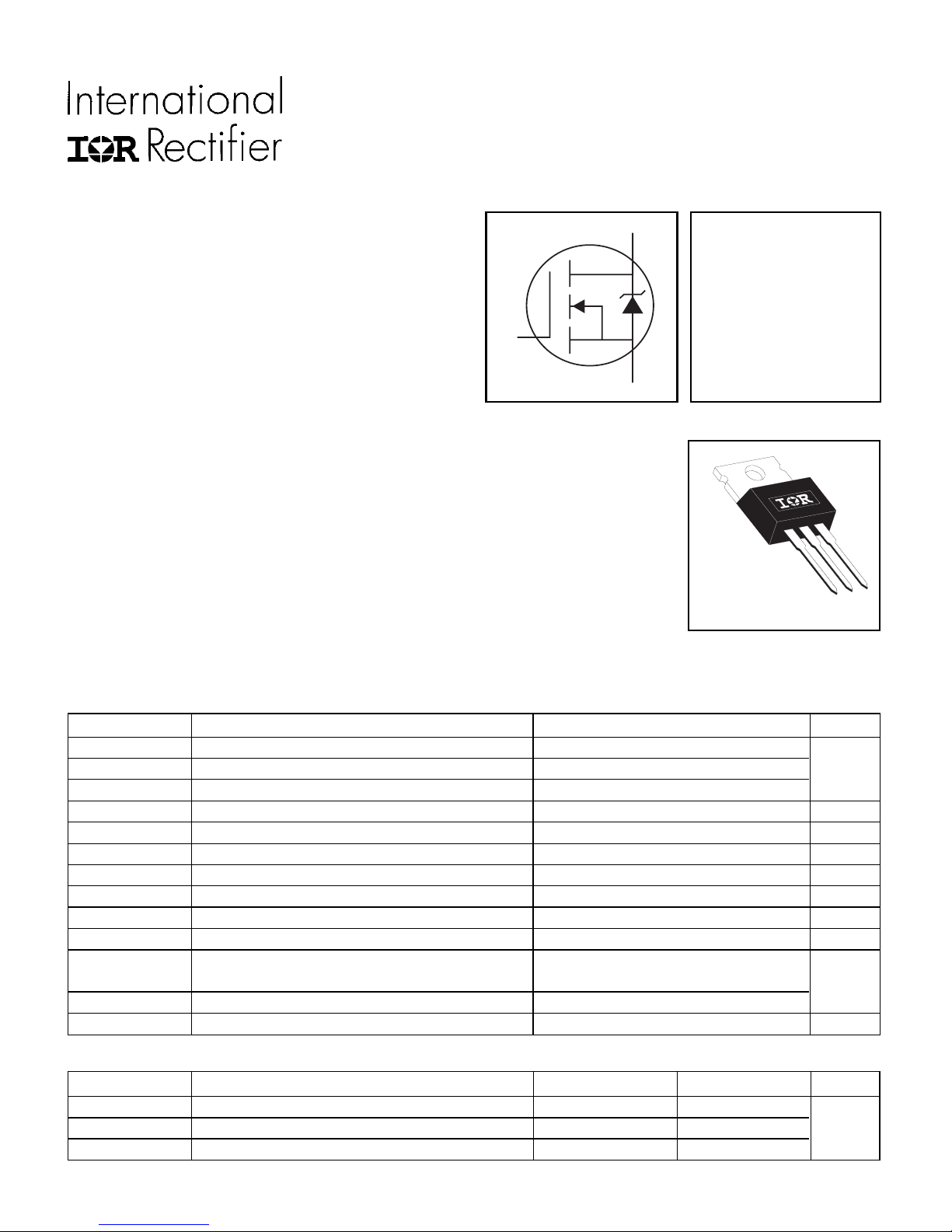
S
D
G
Parameter Max. Units
ID@ TC= 25°C ContinuousDrain Current, VGS @10V 100
ID@ TC= 100°C ContinuousDrain Current,VGS @ 10V 71 A
IDM PulsedDrain Current400
PD @TC= 25°C PowerDissipation 170 W
LinearDeratingFactor 1.11 W/°C
VGS Gate-to-SourceVoltage ± 20 V
EAS SinglePulseAvalancheEnergy350 mJ
IAR AvalancheCurrent60 A
EAR RepetitiveAvalancheEnergy17 mJ
dv/dt Peak Diode Recovery dv/dt 5.0 V/ns
TJOperatingJunctionand -55 to + 175
TSTG Storage Temperature Range
Soldering Temperature, for 10 seconds 300 (1.6mm from case ) °C
Mounting torque, 6-32 or M3 srew 10 lbf•in (1.1N•m)
Absolute Maximum Ratings
Parameter Typ. Max. Units
RθJC Junction-to-Case ––– 0.90
RθCS Case-to-Sink, Flat, Greased Surface 0.50 ––– °C/W
RθJA Junction-to-Ambient ––– 62
Thermal Resistance
VDSS = 40V
RDS(on) = 0.009Ω
ID= 100A
TO-220AB
lAdvanced Process Technology
lUltra Low On-Resistance
lDynamic dv/dt Rating
l175°C Operating Temperature
lFast Switching
lFully Avalanche Rated
Description
4/24/98
www.irf.com 1
PD- 9.1724A
IRF1104
2 www.irf.com
Parameter Min. Typ. Max. Units Conditions
V(BR)DSS Drain-to-Source Breakdown Voltage 40 ––– ––– V VGS = 0V, ID= 250µA
∆V(BR)DSS/∆TJBreakdownVoltageTemp.Coefficient ––– 0.038 ––– V/°C Reference to 25°C, ID= 1mA
RDS(on) StaticDrain-to-SourceOn-Resistance ––– ––– 0.009 ΩVGS = 10V, ID= 60A
VGS(th) Gate Threshold Voltage 2.0 ––– 4.0 V VDS = VGS, ID= 250µA
gfs ForwardTransconductance 37 ––– ––– S VDS = 25V, ID= 60A
––– ––– 25 µA VDS = 40V, VGS = 0V
––– ––– 250 VDS = 32V, VGS = 0V, TJ= 150°C
Gate-to-Source Forward Leakage ––– ––– 100 VGS = 20V
Gate-to-Source Reverse Leakage ––– ––– -100 nA VGS = -20V
QgTotalGateCharge ––– ––– 93 ID= 60A
Qgs Gate-to-SourceCharge ––– ––– 29 nC VDS = 32V
Qgd Gate-to-Drain("Miller")Charge ––– ––– 30 VGS = 10V, See Fig. 6 and 13
td(on) Turn-On Delay Time ––– 15 ––– VDD = 20V
trRiseTime ––– 114 ––– ID= 60A
td(off) Turn-OffDelayTime ––– 28 ––– RG= 3.6Ω
tfFallTime ––– 19 ––– RD= 0.33Ω, See Fig. 10
Between lead,
––– ––– 6mm (0.25in.)
from package
and center of die contact
Ciss Input Capacitance ––– 2900 ––– VGS = 0V
Coss Output Capacitance ––– 1100 ––– pF VDS = 25V
Crss Reverse Transfer Capacitance ––– 250 ––– ƒ = 1.0MHz, See Fig. 5
nH
Electrical Characteristics @ TJ= 25°C (unless otherwise specified)
LDInternal Drain Inductance
LSInternal Source Inductance ––– –––
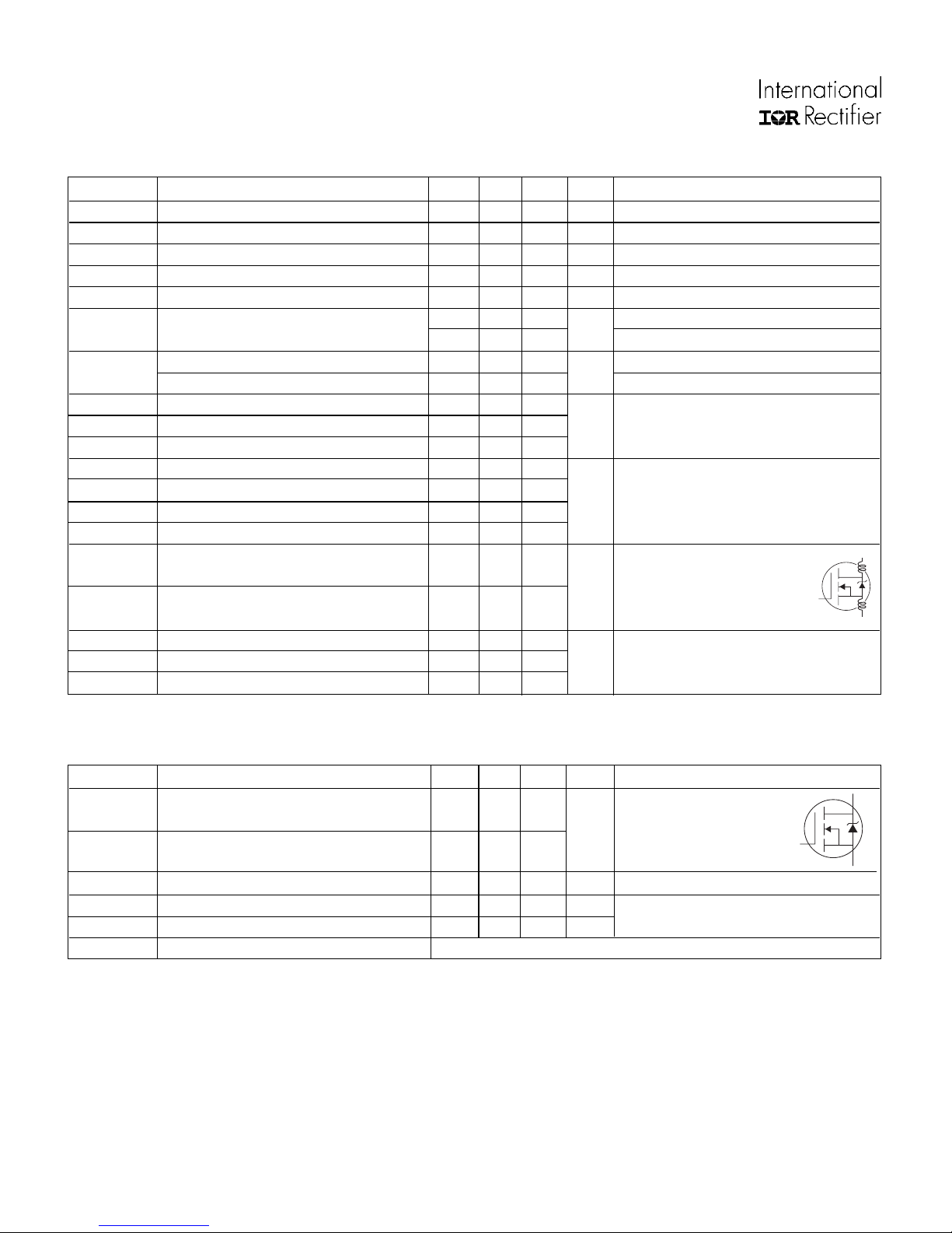
S
D
G
IGSS
ns
4.5
7.5
IDSS Drain-to-Source Leakage Current
Repetitive rating; pulse width limited by
max. junction temperature. ( See fig. 11 )
ISD ≤60A, di/dt ≤304A/µs, VDD ≤ V(BR)DSS,
TJ ≤175°C
Notes:
Starting TJ = 25°C, L = 194µH
RG = 25Ω, IAS = 60A. (See Figure 12)
Pulse width ≤300µs; duty cycle ≤2%.
S
D
G
Parameter Min. Typ. Max. Units Conditions
ISContinuous Source Current MOSFET symbol
(Body Diode) ––– ––– showing the
ISM Pulsed Source Current integral reverse
(Body Diode)
––– ––– p-n junction diode.
VSD DiodeForwardVoltage ––– ––– 1.3 V TJ= 25°C, IS= 60A, VGS = 0V
trr Reverse RecoveryTime ––– 74 110 ns TJ= 25°C, IF= 60A
Qrr ReverseRecoveryCharge ––– 188 280 nC di/dt = 100A/µs
ton Forward Turn-On Time Intrinsic turn-on time is negligible (turn-on is dominated by LS+LD)
Source-Drain Ratings and Characteristics
100
400 A
Caculated continuous current based on maximum allowable
junction temperature;for recommended current-handling of the
package refer to Design Tip # 93-4

IRF1104
www.irf.com 3
Fig 4. Normalized On-Resistance
Vs. Temperature
Fig 2. Typical Output CharacteristicsFig 1. Typical Output Characteristics
Fig 3. Typical Transfer Characteristics
1
10
100
1000
0.1 1 10 100
20µs PULSE WIDTH
T = 175 C
J°
TOP
BOTTOM
VGS
15V
10V
8.0V
7.0V
6.0V
5.5V
5.0V
4.5V
V , Drain-to-Source Voltage (V)
I , Drain-to-Source Current (A)
DS
D
4.5V
1
10
100
1000
0.1 1 10 100
20µs PULSE WIDTH
T = 25 C
J°
TOP
BOTTOM
VGS
15V
10V
8.0V
7.0V
6.0V
5.5V
5.0V
4.5V
V , Drain-to-Source Voltage (V)
I , Drain-to-Source Current (A)
DS
D
4.5V
0.1
1
10
100
1000
4.0 5.0 6.0 7.0 8.0 9.0 10.0
V = 50V
20µs PULSE WIDTH
DS
V , Gate-to-Source Voltage (V)
I , Drain-to-Source Current (A)
GS
D
T = 175 C
J°
T = 25 C
J°
-60 -40 -20 0 20 40 60 80 100 120 140 160 180
0.0
0.5
1.0
1.5
2.0
2.5
T , Junction Temperature( C)
R , Drain-to-Source On Resistance
(Normalized)
J
DS(on)
°
V =
I =
GS
D
10V
100A

IRF1104
4 www.irf.com
Fig 8. Maximum Safe Operating Area
Fig 6. Typical Gate Charge Vs.
Gate-to-SourceVoltage
Fig 5. Typical Capacitance Vs.
Drain-to-SourceVoltage
Fig 7. Typical Source-Drain Diode
Forward Voltage
1 10 100
0
1000
2000
3000
4000
5000
V , Drain-to-Source Voltage (V)
C, Capacitance (pF)
DS
V
C
C
C
=
=
=
=
0V,
C
C
C
f = 1MHz
+ C
+ C
C SHORTED
GS
iss gs gd , ds
rss gd
oss ds gd
Ciss
Coss
Crss
0.1
1
10
100
1000
0.2 0.8 1.4 2.0 2.6
V ,Source-to-Drain Voltage (V)
I , Reverse Drain Current (A)
SD
SD
V = 0 V
GS
T = 25 C
J°
T = 175 C
J°
1
10
100
1000
10000
1 10 100
OPERATION IN THIS AREA LIMITED
BY RDS(on)
Single Pulse
T
T = 175 C
= 25 C
°°
J
C
V , Drain-to-Source Voltage (V)
I , Drain Current (A)I , Drain Current (A)
DS
D
10us
100us
1ms
10ms
025 50 75 100
0
5
10
15
20
Q , Total Gate Charge (nC)
V , Gate-to-Source Voltage (V)
G
GS
FOR TEST CIRCUIT
SEE FIGURE
I =
D
13
60A
V = 20V
DS
V = 32V
DS
IRF1104
www.irf.com 5
Fig 10a. Switching Time Test Circuit
V
DS
90%
10%
V
GS t
d(on)
t
r
t
d(off)
t
f
Fig 10b. Switching Time Waveforms
VDS
Pulse Width ≤ 1 µs
Duty Factor ≤ 0.1 %
RD
VGS
RGD.U.T.
10V
+
-
VDD
Fig 11. Maximum Effective Transient Thermal Impedance, Junction-to-Case
Fig 9. Maximum Drain Current Vs.
Case Temperature
0.01
0.1
1
0.00001 0.0001 0.001 0.01 0.1 1
Notes:
1. Duty factor D = t / t
2. Peak T =P x Z + T
1 2
JDM thJC C
P
t
t
DM
1
2
t , Rectangular Pulse Duration (sec)
Thermal Response (Z )
1
thJC
0.01
0.02
0.05
0.10
0.20
D = 0.50
SINGLE PULSE
(THERMAL RESPONSE)
25 50 75 100 125 150 175
0
20
40
60
80
100
T , Case Temperature ( C)
I , Drain Current (A)
°
C
D
LIMITED BY PACKAGE

IRF1104
6 www.irf.com
Q
G
Q
GS
Q
GD
V
G
Charge
D.U.T. V
DS
I
D
I
G
3mA
V
GS
.3µF
50KΩ
.2µF
12V
Current Regulator
Same Type as D.U.T.
Current Sampling Resistors
+
-
10 V
Fig 13b. Gate Charge Test Circuit
Fig 13a. Basic Gate Charge Waveform
Fig 12c. Maximum Avalanche Energy
Vs. Drain Current
Fig 12b. Unclamped Inductive Waveforms
Fig 12a. Unclamped Inductive Test Circuit
tp
V
(BR)DSS
I
AS
R
G
I
AS
0.01
Ω
t
p
D.U.T
L
VDS
+
-V
DD
DRIVER
A
15V
20V
25 50 75 100 125 150 175
0
200
400
600
800
Starting T , Junction Temperature( C)
E , Single Pulse Avalanche Energy (mJ)
J
AS
°
ID
TOP
BOTTOM
24A
42A
60A
IRF1104
www.irf.com 7
P.W. Period
di/dt
Diode Recovery
dv/dt
Ripple ≤5%
Body Diode Forward Drop
Re-Applied
Voltage
Reverse
Recovery
Current Body Diode Forward
Current
V
GS
=10V
V
DD
I
SD
Driver Gate Drive
D.U.T. I
SD
Waveform
D.U.T. V
DS
Waveform
Inductor Curent
D = P.W.
Period
+
-
+
+
+
-
-
-
Fig 14. For N-Channel HEXFETS
*VGS = 5V for Logic Level Devices
Peak Diode Recovery dv/dt Test Circuit
RGVDD
• dv/dt controlled by RG
• Driver same type as D.U.T.
• ISD controlled by Duty Factor "D"
• D.U.T. - Device Under Test
D.U.T Circuit Layout Considerations
• Low Stray Inductance
• Ground Plane
• Low Leakage Inductance
Current Transformer
*

IRF1104
8 www.irf.com
LEAD ASSIGNMENTS
1 - GATE
2 - DRAIN
3 - SOURCE
4 - DRAIN
- B -
1.32 (.052)
1.22 (.048)
3X 0.55 (.022)
0.46 (.018)
2.92 (.115)
2.64 (.104)
4.69 (.185)
4.20 (.165)
3X 0.93 (.037)
0.69 (.027)
4.06 (.160)
3.55 (.140)
1.15 (.045)
MIN
6.47 (.255)
6.10 (.240)
3.78 (.149)
3.54 (.139)
- A -
10.54 (.415)
10.29 (.405)
2.87 (.113)
2.62 (.103)
15.24 (.600)
14.84 (.584)
14.09 (.555)
13.47 (.530)
3X 1.40 (.055)
1.15 (.045)
2.54 (.100)
2X
0.36 (.014) M B A M
4
1 2 3
NOTES:
1 DIMENSIONING & TOLERANCING PER ANSIY14.5M,1982. 3 OUTLINE CONFORMS TO JEDEC OUTLINE TO-220AB.
2 CONTROLLING DIMENSION : INCH 4 HEATSINK & LEAD MEASUREMENTS DO NOT INCLUDE BURRS.
Part Marking Information
TO-220AB
Package Outline
TO-220AB Outline
Dimensions are shown in millimeters (inches)
PART NUMBER
INTERNATIONAL
RECTIFIER
LOGO
EXAMPLE : THIS IS AN IRF1010
WITH ASSEMBLY
LOT CODE 9B1M
ASSEMBLY
LOT CODE
DATE CODE
(YYWW)
YY = YEAR
WW = WEEK
9246
IRF1010
9B 1M
A
WORLD HEADQUARTERS: 233 Kansas St., El Segundo, California 90245, Tel: (310) 322 3331
EUROPEAN HEADQUARTERS: Hurst Green, Oxted, Surrey RH8 9BB, UK Tel: ++ 44 1883 732020
IR CANADA: 7321 Victoria Park Ave., Suite 201, Markham, Ontario L3R 2Z8, Tel: (905) 475 1897
IR GERMANY: Saalburgstrasse 157, 61350 Bad Homburg Tel: ++ 49 6172 96590
IR ITALY: Via Liguria 49, 10071 Borgaro, Torino Tel: ++ 39 11 451 0111
IR FAR EAST: K&H Bldg., 2F, 30-4 Nishi-Ikebukuro 3-Chome, Toshima-Ku, Tokyo Japan 171 Tel: 81 3 3983 0086
IR SOUTHEAST ASIA: 315 Outram Road, #10-02 Tan Boon Liat Building, Singapore 0316 Tel: 65 221 8371
http://www.irf.com/ Dataand specifications subject to changewithout notice. 4/98
This manual suits for next models
1
Table of contents


