General description
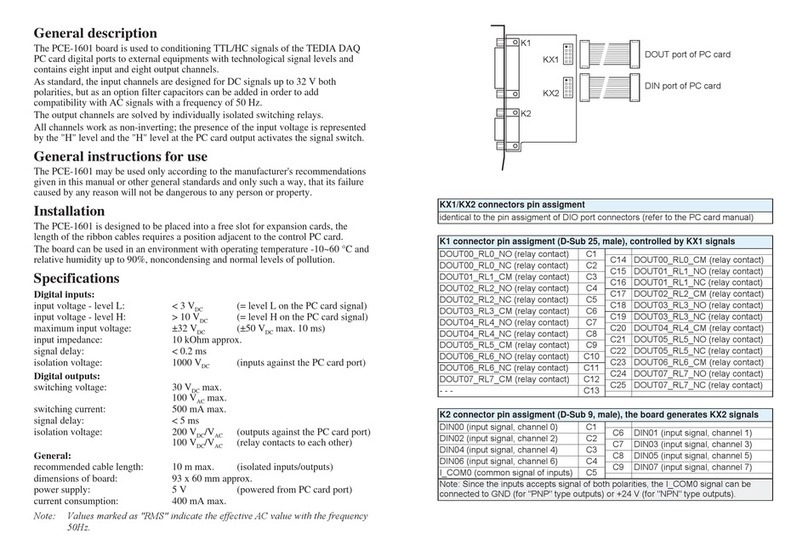
The PCE-1613 board is used to conditioning TTL/HC signals of the TEDIA DAQ
PC card digital ports to external equipments with technological signal levels and
contains eight input channels and one 8-bit DIO port without conditioning.
As standard, the input channels are designed for DC signals up to 32 V both
polarities, but as an option filter capacitors can be added in order to add
compatibility with AC signals with a frequency of 50 Hz.
All channels work as non-inverting; the presence of the input voltage is represented
by the "H" level on the PC card signal.
For eight pass-through signals (ie. one 8-bit DIO port), the PCE-1613 board
performs the function of adapter the PC card connector to the D-Sub 9 connector
located on the mounting bracket. The board does not provide any conditioning to
these signals.
General instructions for use
The PCE-1613 may be used only according to the manufacturer's recommendations
given in this manual or other general standards and only such a way, that its failure
caused by any reason will not be dangerous to any person or property.
Installation
The PCE-1613 is designed to be placed into a free slot for expansion cards, the
length of the ribbon cables requires a position adjacent to the control PC card.
The board can be used in an environment with operating temperature -10~60 °C and
relative humidity up to 90%, noncondensing and normal levels of pollution.
Specifications
Digital inputs:
input voltage - level L: < 3 VDC (= level L on the PC card signal)
input voltage - level H: > 10 VDC (= level H on the PC card signal)
maximum input voltage: ±32 VDC (±50 VDC max. 10 ms)
input impedance: 10 kOhm approx.
signal delay: < 0.2 ms
isolation voltage: 1000 VDC (inputs against the PC card port)
General:
recommended cable length: 10 m max. (isolated inputs)
2 m max. (nonisolated PC card port)
dimensions of board: 80 x 60 mm approx.
power supply: 5 V (powered from PC card port)
current consumption: 20 mA max.
KX1/KX2 connectors pin assigment
identical to the pin assigment of DIO port connectors (refer to the PC card manual)
K1 connector pin assigment (D-Sub 9, male), connected to KX1 signals
DIO0 (I/O signal of card DIO port) C1 C6 DIO1 (signal of card DIO port)
DIO2 (I/O signal of card DIO port) C2 C7 DIO3 (I/O signal of card DIO port)
DIO4 (I/O signal of card DIO port) C3 C8 DIO5 (I/O signal of card DIO port)
DIO6 (I/O signal of card DIO port) C4 C9 DIO7 (I/O signal of card DIO port)
GND (computer GND) C5
K2 connector pin assigment (D-Sub 9, male), the board generates KX2 signals
DIN00 (input signal, channel 0) C1 C6 DIN01 (input signal, channel 1)
DIN02 (input signal, channel 2) C2 C7 DIN03 (input signal, channel 3)
DIN04 (input signal, channel 4) C3 C8 DIN05 (input signal, channel 5)
DIN06 (input signal, channel 6) C4 C9 DIN07 (input signal, channel 7)
I_COM0 (common signal of inputs) C5
Note: Since the inputs accepts signal of both polarities, the I_COM0 signal can be
connected to GND (for "PNP" type outputs) or +24 V (for "NPN" type outputs).
K1
K2
KX1
KX2 DIN port of PC card
DIO port of PC card


