International Rectifier SupIRBuck IRDC3846 User manual

IRDC3846-P1V2
Confidential
This evaluation board is a preliminary version meant for the engineering evaluation of the IR3846. Based on the results
of the continuing evaluation, this board can evolve and change without notice
AL
4/11/2013 1
USER GUIDE FOR IR3846 EVALUATION BOARD
DESCRIPTION
The IR3846 is a synchronous buck
converter, providing a compact, high
performance and flexible solution in a small
5mmx7mm QFN package.
Key features offered by the IR3846 include
internal Digital Soft Start, precision 0.6V
reference voltage, Power Good, thermal
protection, programmable switching
frequency, Enable input, input under-voltage
lockout for proper start-up, enhanced line/
load regulation with feed forward, external
frequency synchronization with smooth
clocking, internal LDO, true differential
remote sensing and pre-bias start-up.
A thermally compensated output over-current
protection function is implemented by sensing
the voltage developed across the on-resistance
of the synchronous rectifier MOSFET for
optimum cost and performance.
This user guide contains the schematic and bill
of materials for the IR3846 evaluation board.
The guide describes operation and use of the
evaluation board itself. Detailed application
information for IR3846 is available in the
IR3846 data sheet.
BOARD FEATURES
•Vin = +12V (+ 13.2V Max), No Vcc required.
•Vout = +1.2V @ 0-35A
•Fs=600kHz
•L= 0.250uH
•Cin= 7x22uF (ceramic 1206) + 1x330uF (electrolytic)
•Cout= 6x100uF (ceramic 1206)
SupIRBuckTM
IRDC3846-P1V2
Confidential
This evaluation board is a preliminary version meant for the engineering evaluation of the IR3846. Based on the results
of the continuing evaluation, this board can evolve and change without notice
AL
4/11/2013 2
A well regulated +12V input supply should be connected to VIN+ and VIN-. A maximum of 35A load should
be connected to VOUT+ and VOUT-. The inputs and output connections of the board are listed in Table I.
IR3846 needs only one input supply and internal LDO generates Vcc from Vin. If operation with external Vcc
is required, then R3 should be removed and external Vcc can be applied between Vcc+ and Vcc- pins. Vin
pin and Vcc pins should be shorted together for external Vcc operation by installing a 0 ohm resistor at R4.
The board is configured for remote sensing. If local sense is desired, R18 should be uninstalled and R19
should be installed instead.
External Enable signal can be applied to the board via exposed Enable pad and R100 should be removed
for this purpose.
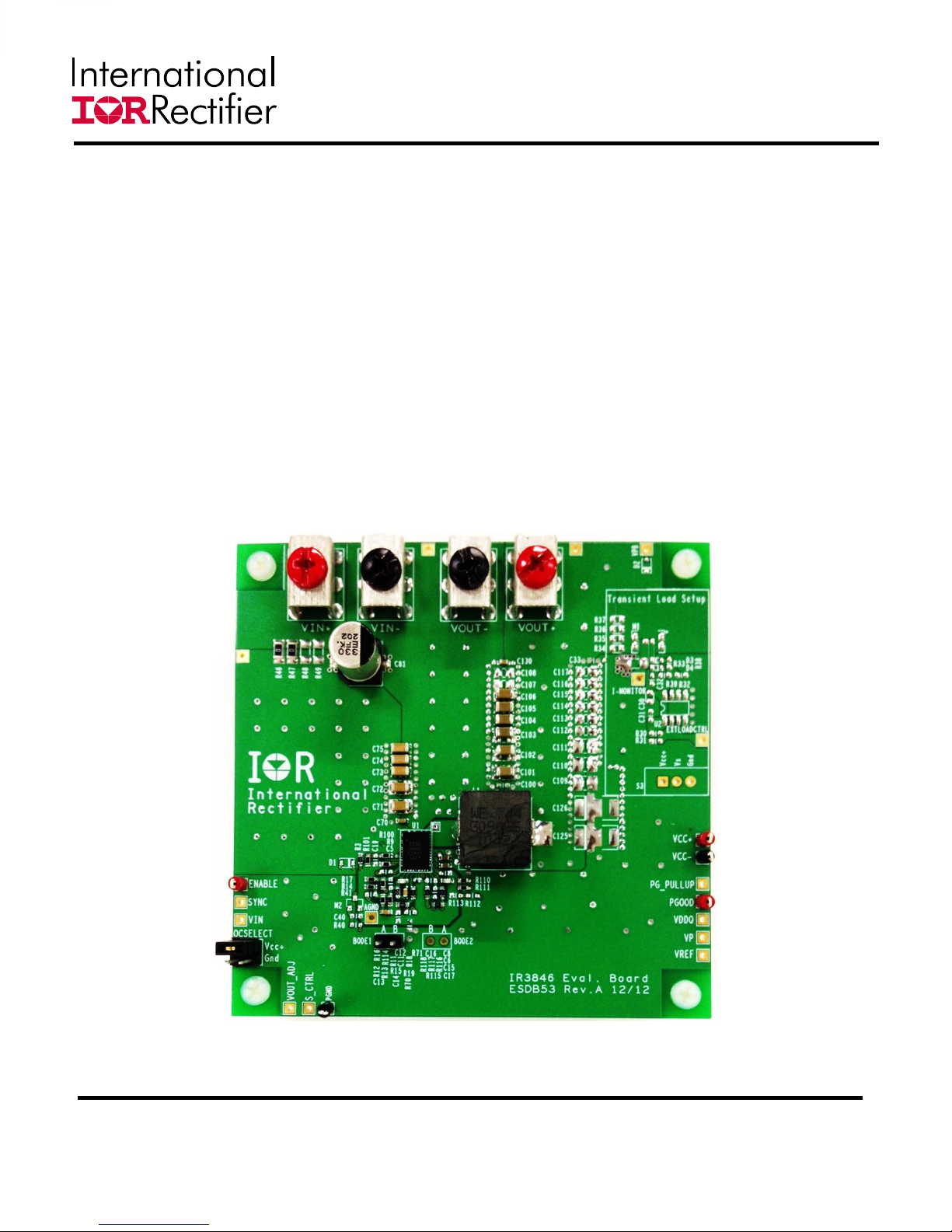
CONNECTIONS and OPERATING INSTRUCTIONS
LAYOUT
The PCB is a 6-layer board. All of layers are 2 Oz. copper. The IR3846 and most of the passive
components are mounted on the top side of the board.
Power supply decoupling capacitors and feedback components are located close to IR3846. The
feedback resistors are connected to the output of the remote sense amplifier of the IR3846 and are
located close to the IR3846. To improve efficiency, the circuit board is designed to minimize the length
of the on-board power ground current path. Separate power ground and analog ground are used and
may be connected together using a 0 ohm resistor at R71.
Table I. Connections
Connection Signal Name
VIN+ Vin (+12V)
VIN- Ground of Vin
Vout+ Vout(+1.2V)
Vout- Ground for Vout
Vcc+ Vcc Pin
Vcc- Ground for Vcc input
Enable Enable
PGood Power Good Signal
AGnd Analog ground
IRDC3846-P1V2
Confidential
This evaluation board is a preliminary version meant for the engineering evaluation of the IR3846. Based on the results
of the continuing evaluation, this board can evolve and change without notice
AL
4/11/2013 3
CONNECTIONS and OPERATING INSTRUCTIONS
LAYOUT
The PCB is a 6-layer board. All of layers are 2 Oz. copper. The IR3846 and most of the passive
components are mounted on the top side of the board.
Power supply decoupling capacitors and feedback components are located close to IR3846. The
feedback resistors are connected to the output of the remote sense amplifier of the IR3846 and are
located close to the IR3846. To improve efficiency, the circuit board is designed to minimize the length
of the on-board power ground current path. Separate power ground and analog ground are used and
may be connected together using a 0 ohm resistor at R71.
Vin Vo
Gnd Gnd
Top View
IRDC3846-P1V2
Confidential
This evaluation board is a preliminary version meant for the engineering evaluation of the IR3846. Based on the results
of the continuing evaluation, this board can evolve and change without notice
AL
4/11/2013 4
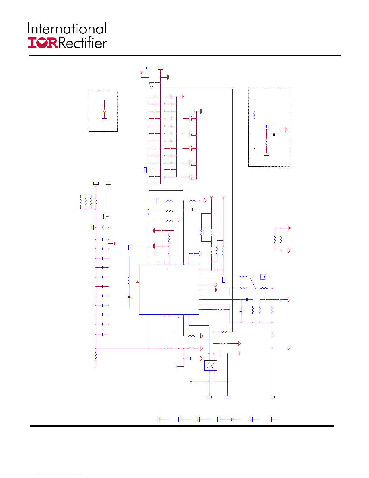
Fig. 1: Schematic of the IR3846 evaluation board
Single point of connection between Power
Ground and Signal ( “analog” ) Ground
Vref
S_Ct rl
1
C130
0.1uF
R112
N/S
M2
N/S
R113
N/S
BODE1
JUMPER 2
L1 250nH WE744309025
PGD
RT/Sy nc
R70N/S
Vout+
123456
Vin
1
R1160
C16
N/S
Optional "1-bit VID" circuit
OCSelec t
4pin jumper
1
2 3
4
Vp
Vout
C119
N/S
C120
N/S
C121
N/S
C122
N/S
Optional Pre-Bias test circuit
C123
N/S
FB
C124
N/S
C14
N/S
Sy nc
Vout
R100
C11
8.2nF
VPB
1
R114
N/S
R101
7.5K
SW
1
C77
22uF
R112.7K
C79
N/S
R19
N/S
R12127
R134.02K
C114
N/S
C78
N/S
R15
20
Vsns
PVin
C113
N/S
R48
N/S
C108
N/S
C107
N/S
R49N/S
C106
100uF
PGD
U1
IR3846
Vref 17
RSo
11
BOOT
4
NC3 22
Vp 18
Vsns
8
RT/Sy nc
6
Enable
5
OCset
7
NC1
2
RS+
16
PVin
1
Comp
10
PGND
12
LGND
13
FB
9
VCC 21
NC4 23
Vin 20
SW 24
S_Ct rl
14
RS-
15
NC2
3
PGD 19
NC5 26
R1150
C105
100uF
+
C125
N/S
PVin
C73
22uF
C70
0.1uF
BODE2
JUMPER 3
C72
22uF
C71
22uF
C76
22uF
7 x 22uF / 1206 / 25V / Ceramic Capacitor
6 x 100uF / 1206 / 6.3V / Ceramic Capacitor
330uF / 25V / Electrolytic Capacitor
+
C126
N/S
BOOT
R17
4.02K
Vcc-
1
+
C127
N/S
D2N/S
1 2
D1
N/S
12
Vsns
R100
49.9K
+
C81
330uF
+
C128
N/S
R30
PVin
C115
N/S
C104
100uF
PG_PU
VCC
C112
N/S
C13
2200pF
C74
22uF
Rt/Sync
R9
39.2K
C80
N/S
C15
N/S
+
C129
N/S
R16
4.02K
C8
10uF
C6
1uF
Vin
Agnd
1
C103
100uF
Vout
R1180
C102
100uF
R117
N/S
PG_PU
PG_Pullup
1
C101
100uF
Vo_R_P
R144.02K
C71-C80: 0805 / 1206 pads
R46-R49: 1206 pads
C100-C124: 0805 / 1206 pads
C19
N/S
R710
R470
VCC
C109
N/S
Vout-
123456
Vin
R460
Vcc+
1
FB
PGood
1
Vout_Adj
1
C12160pF
R4N/S
R40N/S
R41N/S
Vo_R_N
C40
N/S
C110
N/S
R111
10K
FB
C5
N/S
C17
100pF
Vref
Vin
1
Vref
1
Vin
C75
22uF
R18
0
C111
N/S
VCC
VCC C116
N/S
Sy nc
1
Enable
1
BOOT
R110
10K
C117
N/S
C100.1uF
Vp
C118
N/S
Vin+
123456
Vin-
123456
Vin
1
Vp
1
Vin
1
VDDQ
1
C100
N/S
Vin
1
IRDC3846-P1V2
Confidential
This evaluation board is a preliminary version meant for the engineering evaluation of the IR3846. Based on the results
of the continuing evaluation, this board can evolve and change without notice
AL
4/11/2013 5
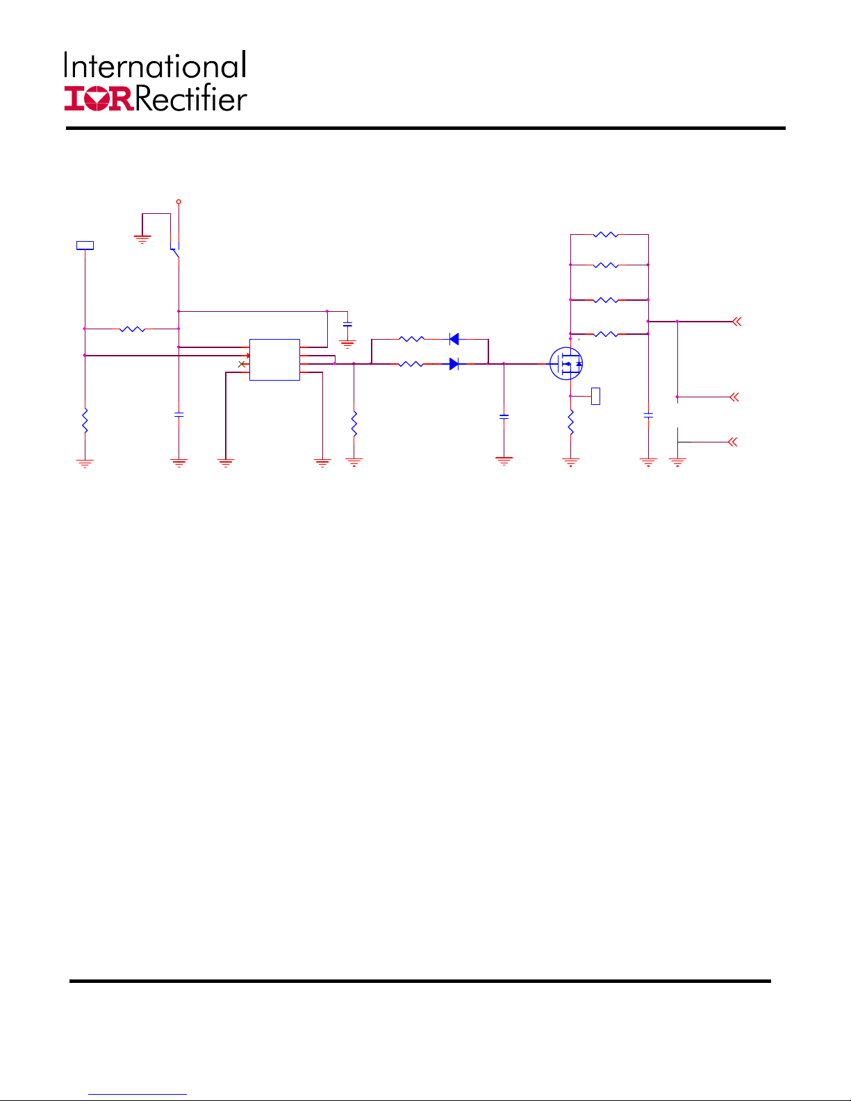
Schematic for Transient Load set up
N/S
R33
N/S
Vout
C30
N/S
R34N/S
R35N/S
R36N/S
R37N/S
ExtLoadCtrl
1
M1
IRF6721 N/S
U2
MIC4452/SO8 N/S
VS
1
IN
2
GND
4GND 5
OUT1 6
OUT2 7
VS 8
N/A
3
R30N/S
R32
N/S
S3
SW
2 1
3
C33
N/S
C31
N/S
R31
N/S
Vout
C32
N/S
Vo_R_P
D4
N/S
D3
N/S
R38N/S
R39N/S
Vo_R_N
Optional transient load circuit
VCC
I-Monitor
1
IRDC3846-P1V2
Confidential
This evaluation board is a preliminary version meant for the engineering evaluation of the IR3846. Based on the results
of the continuing evaluation, this board can evolve and change without notice
AL
4/11/2013 6
Bill of Materials
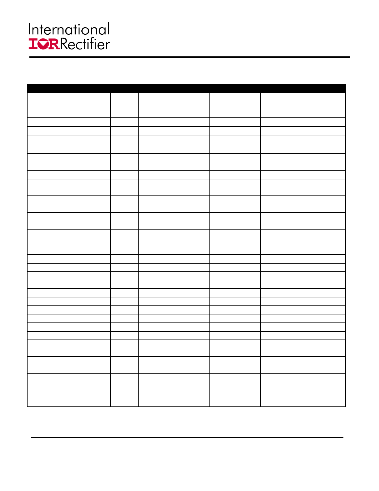
Item Qty Part Reference Value Description Manufacturer Part Number
17
C71 C72 C73
C74 C75 C76
C77
22uF 1206, 25V, X5R, 10% Murata GRM31CR61E226KE15L
21C6 1uF 0603, X5R, 25V, 20% TDK C1608X5R1E105M
31C8 10uF 0603, X5R, 10V, 20% TDK C1608X5R1A106M
43 C10 C70 C130 0.1uF 0603, 25V, X7R, 10% Murata GRM188R71E104KA01D
51 C11 8200pF 0603, 50V, X7R, 10% Murata GRM188R71H822KA01D
61 C12 160pF 0603, 50V, NP0, 5% Murata GRM1885C1H161JA01D
71 C13 2200pF 0603, 50V, X7R, 10% Murata GRM188R71H222KA01D
81 C17 100pF 0603, 50V, C0G, 5% Murata GRM1885C1H101JA01D
91 C81 330uF SMD Elecrolytic, Fsize,
25V, 20% Panasonic EEV-FK1E331P
10 1 L1 250nH 250nH,
DCR=0.165mohm
Wurth
Electronics Inc. 744309025
11 6 C101 C102 C103
C104 C105 C106 100uF 1206, 6.3V, X5R, 20% Murata GRM31CR60J107ME39L
12 6R3 R10 R18
R115 R116 R118 0 0603,1/10W, Jumper Vishay/Dale CRCW06030000Z0EA
13 1 R9 39.2K 0603,1/10W,1% Panasonic ERJ-3EKF3922V
14 1 R11 2.7K 0603,1/10W,1% Panasonic ERJ-3EKF2701V
15 1 R12 127 0603,1/10W,1% Panasonic ERJ-3EKF1270V
16 4R13 R14 R16
R17 4.02 K 0603,1/10W,1% Panasonic ERJ-3EKF4021V
17 1 R15 20 0603,1/10W,1% Vishay/Dale CRCW060320R0FKEA
18 2 R46 R47 0 1206,1/4W, Jumper Yageo RC1206JR-070RL
19 1 R71 0 0402, 1/16W, Jumper Yageo RC0402JR-070RL
20 1 R100 49.9K 0603,1/10 W,1% Panasonic ERJ-3EKF4992V
21 1 R101 7.5K 0603,1/10W,1% Panasonic ERJ-3EKF7501V
22 2 R110 R111 10K 0603,1/10 W,1% Panasonic ERJ-3EKF1002V
23 1 Jumper PLUG 40 POS DBL
ROW STR
Omron
Electronics Inc. XG8W-4041-ND
24 2 Vin+ Vout+ RED SCREW TERMINAL Keystone
Electronics 8199-2
25 2 Vin- Vout- BLACK SCREW TERMINAL Keystone
Electronics 8199-3
26 1 U1 IR3846 IR3846 5mm X 7mm International
Rectifier IR3846MPBF
IRDC3846-P1V2
Confidential
This evaluation board is a preliminary version meant for the engineering evaluation of the IR3846. Based on the results
of the continuing evaluation, this board can evolve and change without notice
AL
4/11/2013 7
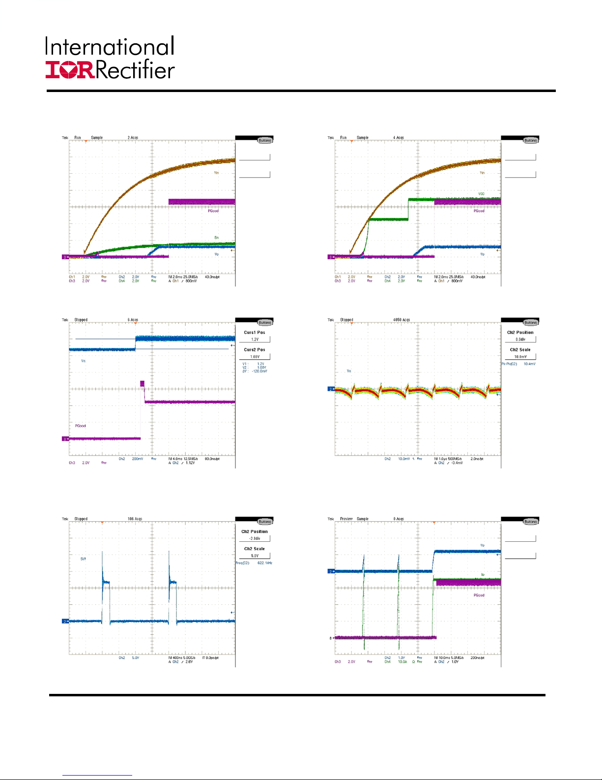
TYPICAL OPERATING WAVEFORMS
Vin=12.0V, Vo=1.2V, Io=0A-35A, Fsw=600kHz, Room Temperature, No air flow
Fig. 5: Output Voltage Ripple, 35A load
Ch1: Vo
Fig. 6: Inductor node at 35A load
Ch2:LX
Fig. 7: Short (Hiccup) Recovery
Ch2:Vo, Ch3:PGood, Ch4:Io
Fig. 3: Start up at 35A Load
Ch1:Vin, Ch2:Vo, Ch3:PGood, Ch4:Vcc
Fig. 2: Start up at 35A Load
Ch1:Vin, Ch2:Vo, Ch3:PGood, Ch4:Enable
Fig. 4: Start up with 1.08V Pre Bias, 0A Load
Ch2:Vo, Ch3:PGood

IRDC3846-P1V2
Confidential
This evaluation board is a preliminary version meant for the engineering evaluation of the IR3846. Based on the results
of the continuing evaluation, this board can evolve and change without notice
AL
4/11/2013 8
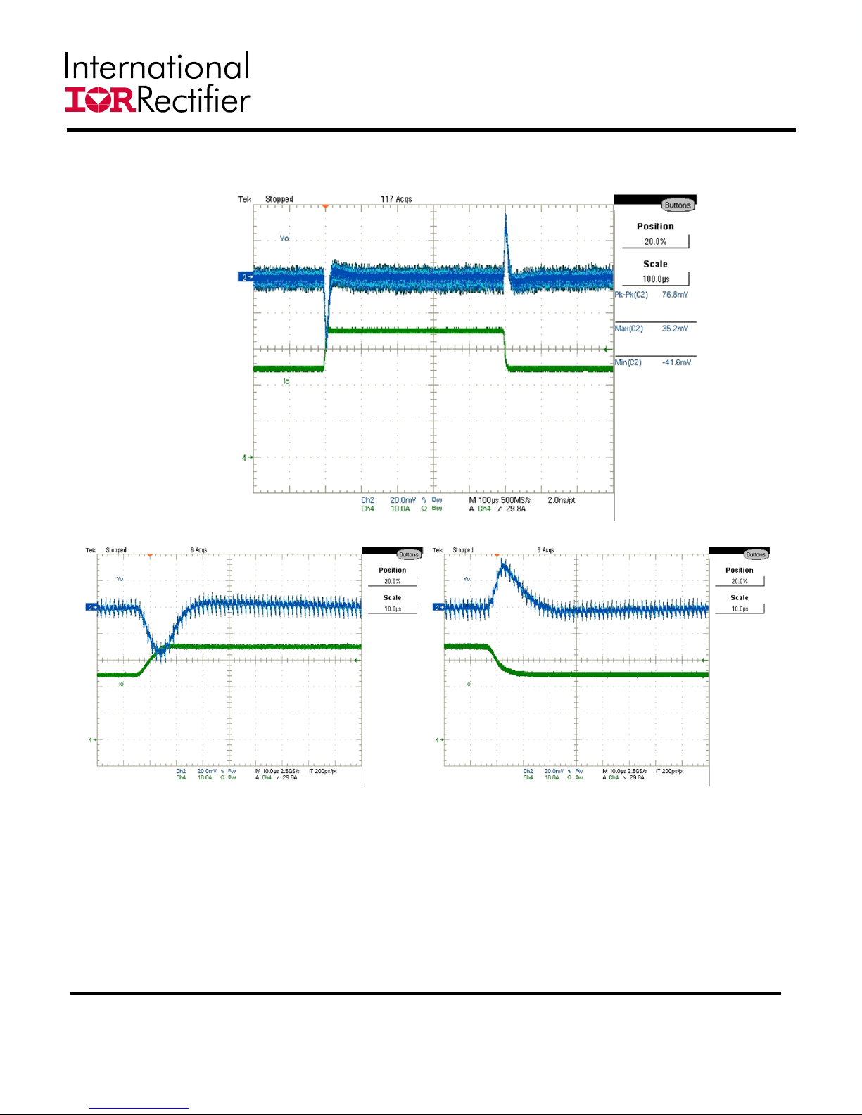
TYPICAL OPERATING WAVEFORMS
Vin=12.0V, Vo=1.2V, Io=3.5A-14A, Fsw=600kHz, Room Temperature, No air flow
Fig. 8: Transient Response, 3.5A to 14A step (2.5A/us)
Ch2:Vo
IRDC3846-P1V2
Confidential
This evaluation board is a preliminary version meant for the engineering evaluation of the IR3846. Based on the results
of the continuing evaluation, this board can evolve and change without notice
AL
4/11/2013 9
TYPICAL OPERATING WAVEFORMS
Vin=12.0V, Vo=1.2V, Io=24.5A-35.0A, Fsw=600kHz, Room Temperature, No air flow
Fig. 9: Transient Response, 24.5A to 35A step (2.5A/us)
Ch2:Vo
IRDC3846-P1V2
Confidential
This evaluation board is a preliminary version meant for the engineering evaluation of the IR3846. Based on the results
of the continuing evaluation, this board can evolve and change without notice
AL
4/11/2013 10
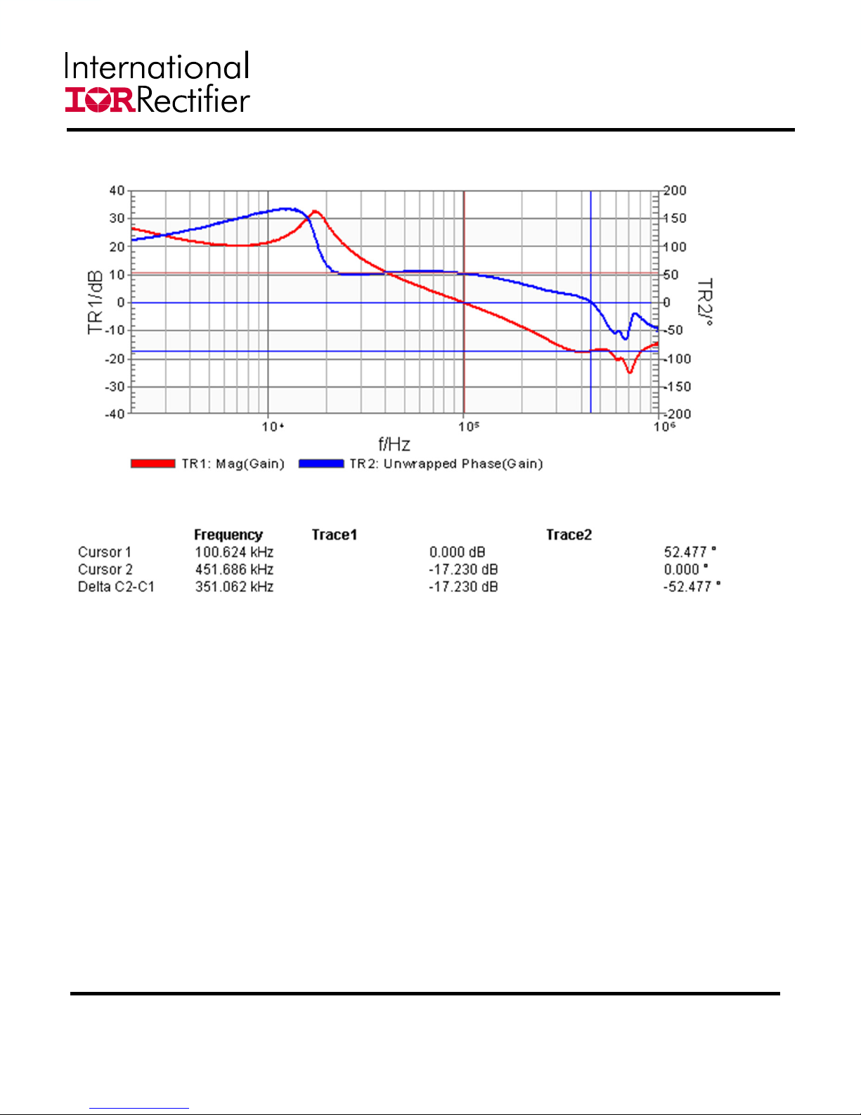
TYPICAL OPERATING WAVEFORMS
Vin=12.0V, Vo=1.2V, Io=0A-35A, Fsw=600kHz, Room Temperature, No air flow
Fig. 10: Bode Plot at 35A load: Fo = 100.6kHz; Phase Margin = 52.8º; Gain Margin = -17.2dB

IRDC3846-P1V2
Confidential
This evaluation board is a preliminary version meant for the engineering evaluation of the IR3846. Based on the results
of the continuing evaluation, this board can evolve and change without notice
AL
4/11/2013 11
Fig.12: Power loss versus load current
Fig.11: Efficiency versus load current
TYPICAL OPERATING WAVEFORMS
Vin=12.0V, Vo=1.2V, Io=0A-35A, Fsw=600kHz, Room Temperature, No air flow
71
73
75
77
79
81
83
85
87
89
91
0 5 10 15 20 25 30 35
Efficiency [%]
Io [A]
0.0
0.5
1.0
1.5
2.0
2.5
3.0
3.5
4.0
4.5
5.0
5.5
6.0
6.5
7.0
7.5
0 5 10 15 20 25 30 35
Power Loss [W]
Io [A]
IRDC3846-P1V2
Confidential
This evaluation board is a preliminary version meant for the engineering evaluation of the IR3846. Based on the results
of the continuing evaluation, this board can evolve and change without notice
AL
4/11/2013 12
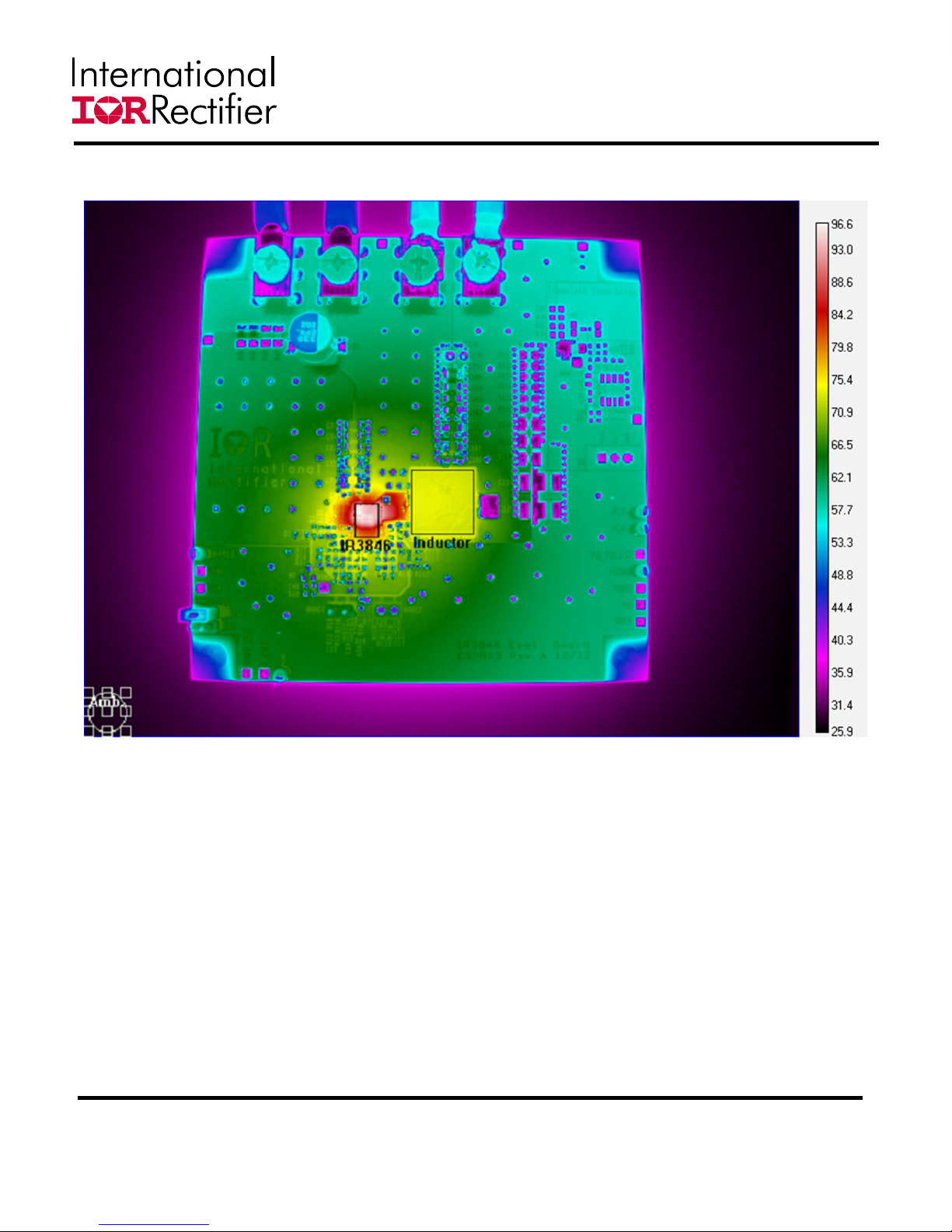
THERMAL IMAGES
Vin=12.0V, Vo=1.2V, Io=35A, Fsw=600kHz, Room Temperature, No air flow
Fig. 13: Thermal Image of the board at 35A load
Test point 1 is IR3846: 98.80C
Test point 2 is inductor: 72.90C
IRDC3846-P1V2
Confidential
This evaluation board is a preliminary version meant for the engineering evaluation of the IR3846. Based on the results
of the continuing evaluation, this board can evolve and change without notice
AL
4/11/2013 13
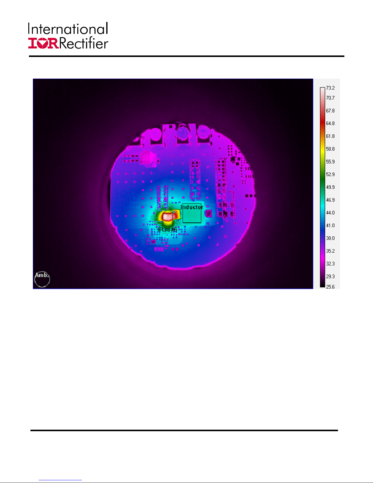
THERMAL IMAGES
Vin=12.0V, Vo=1.2V, Io=35A, Fsw=600kHz, Room Temperature, LFM = 100
Fig. 14: Thermal Image of the board at 35A load
Test point 1 is IR3846: 740C
Test point 2 is inductor: 46.90C

IRDC3846-P1V2
Confidential
This evaluation board is a preliminary version meant for the engineering evaluation of the IR3846. Based on the results
of the continuing evaluation, this board can evolve and change without notice
AL
4/11/2013 14
IR WORLD HEADQUARTERS: 233 Kansas St., El Segundo, California 90245, USA Tel: (310) 252-7105
TAC Fax: (310) 252-7903
Visit us at www.irf.com for sales contact information
Data and specifications subject to change without notice. 4/13
Table of contents
Other International Rectifier Motherboard manuals

International Rectifier
International Rectifier IRDC38063-P1V2 User manual

International Rectifier
International Rectifier IR3651 User manual

International Rectifier
International Rectifier IRDC3847-P1V2 User manual

International Rectifier
International Rectifier IR3847 User manual

International Rectifier
International Rectifier IRS27951 User manual

International Rectifier
International Rectifier IRU3038 User manual

International Rectifier
International Rectifier SupIRBuck IRDC3863 User manual

International Rectifier
International Rectifier IRU3065 User manual

International Rectifier
International Rectifier IRU3046 User manual

International Rectifier
International Rectifier IR3621 User manual


 user manual")


