AN1850 Rev.1.01 Page 2 of 15
Oct 24, 2022
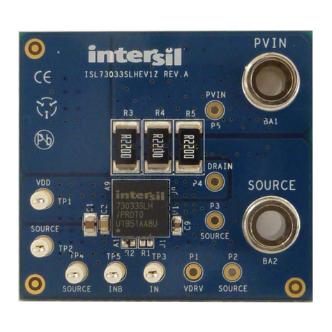
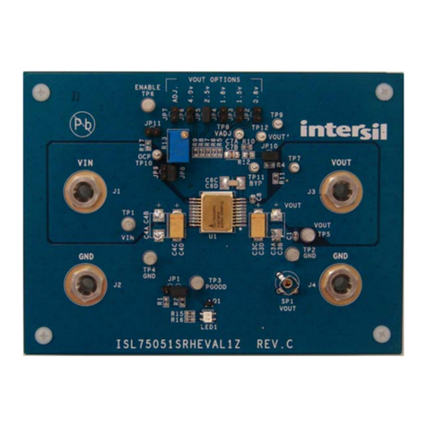
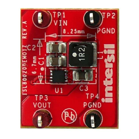
ISL75052SEHEVAL1Z
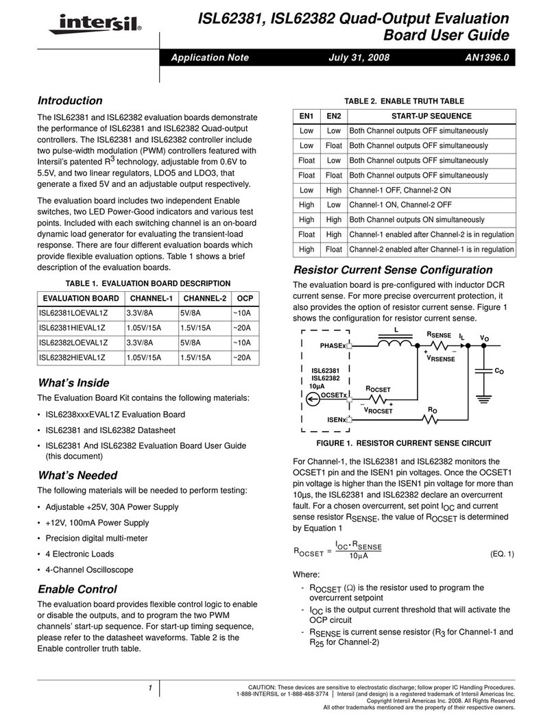
What’s Inside
Items shipped with board:
• ISL75052SEHEVAL1Z evaluation board
• ISL75052SEH datasheet
• AN1850 application note
Test Steps
1. Select the desired output voltage by shorting one of the
jumpers from J1 through J5. The option of JP6 provides for
continuous adjustment of VOUT using potentiometer R6.
2. Set the OCP limit by using jumpers JP8 and JP9.
JP9 = 0.275A min, and JP8 = 2.75A min.
3. Close JP7. Also closing jumper JP11 (2 and 3) selects
R16 = 5.49k as pull-up for PGOOD. Close JP12 (1 and 2).
4. Connect the input supply to VIN/GND and the load to
VOUT/GND. Select the VIN to VOUT ratio to keep dissipation
within the thermal limits of the device.
5. Use JP10 to enable/disable the IC; Open = Enable, and
Close = Disable. (Note: For REVB boards, Close = Enable and
Open = Disable.)
Optimizing LDO Performance
Performance of the ISL75052SEH can be optimized by following
the guidelines provided in this application note.
Input and Output Capacitor Selection
RH operation requires the use of a combination of tantalum and
ceramic capacitors to achieve a good volume-to-capacitance
ratio. The recommended combination is a 2x100µF, 60mΩ, 25V
KEMET T541 series tantalum capacitor in parallel with a 0.1µF
MIL-PRF-49470 CDR04 ceramic capacitor. This is to be
connected between VIN to GND pins and VOUT to GND pins of the
LDO, with PCB traces no longer than 0.5cm. The stability of the
device depends on the capacitance and ESR of the output
capacitor. The usable ESR range for the device is 6mΩto
100mΩ. At the lower limit of ESR = 6mΩ, the phase margin is
about 51°C. On the high side, an ESR of 100mΩis found to limit
the gain margin at around 10dB. The typical GM/PM seen on the
ISL75052SEHEVAL1Z evaluation board for VIN = 3.3V,
VOUT = 1.8V, and IOUT = 3A, with a 220µF, 10V, 25mΩcapacitor,
is GM = 16.3dB, and PM = 69.16°C.
Output Voltage Adjustment
The output voltage can be adjusted by means of the resistor
divider shown in Figure 1 as RTOP and RBOTTOM.
The resistor values for typical output voltages are given in
Table 1. The values listed provide for an evaluation board output
voltage that is about 50mV higher than the desired set point to
allow for the drop on the line connecting the evaluation board to
the desired load.
The resistor divider values can be calculated using the equation:
VOUT = (0.6X(1+RTOP/RBOTTOM)
Assuming a value RTOP = 15.8k and knowing the required output
voltage setting one can calculate the RBOTTOM.
Output Voltage Soft-Start Adjustment
The output voltage soft-start can be adjusted by means of the
capacitor value on the BYP pin, examples are shown in Figure 28
and Figure 29. The BYP cap being 0.2µF and 1.9µF, respectively.
Output Voltage Start-Up Delay Adjustment
The output voltage start can be adjusted by means of the capacitor
value on the VCCX pin examples shown in Figure 28 and Figure 30.
The VCCX cap being 0.1µF and 33µF, respectively.
Layout Guidelines
Good PCB layout is important to achieving expected
performance. When placing components and routing traces,
minimize ground impedance and keep parasitic inductance low.
Give the input and output capacitors a good ground connection,
and place them as close to the IC as possible. Route the traces
connecting the ADJ pin away from noisy planes and traces, and
keep the board capacitance of the ADJ net to GND as low as
possible.
Thermal Guidelines
If the die temperature exceeds +175°C typical, then the LDO
output shuts down to zero until the die temperature cools to
+155°C typical. The level of power combined with the thermal
impedance of the package (JC of 4°C/W for the 18 Ld CDFP
package) determines whether the junction temperature exceeds
the thermal shutdown temperature specified in the “Electrical
Specifications” table of the ISL75052SEH datasheet. Mount the
device on a high effective thermal conductivity PCB with thermal
vias, per JESD51-7 and JESD51-5. Place a silpad between the
package base and the PCB copper plane. Select the VIN and VOUT
ratios to ensure that dissipation for the selected VIN range keeps
TJwithin the recommended operating level of 150°C for normal
operation.
TABLE 1. RECOMMENDED OUTPUT CAPACITOR VALUES
VOUT
(V)
RTOP
(kΩ)
RBOTTOM
(kΩ)
COUT
(µF)
10.0 15.8 1.0 200
9.0 15.8 1.13 200
5.0 15.8 2.15 200
4.0 15.8 2.74 200
2.5
(Note 1)
15.8 4.87 47
2.5 15.8 4.87 200
NOTE:
1. Either option could be used depending on cost/performance
requirements.


