AN1667 Rev.0.00 Page 2 of 15
January 17, 2012
ISL75051SRHEVAL1Z AN1667.0
Optimizing LDO Performance
Performance of the ISL75051SRH can be optimized by following
the guidelines provided in this application note.
Input and Output Capacitor Selection
RH operation requires the use of a combination of tantalum and
ceramic capacitors to achieve a good volume-to-capacitance
ratio. The recommended combination is a 220µF, 25mΩ, 10V
DSSC 04051-032 rated tantalum capacitor in parallel with a
0.1µF MIL-PRF-49470 CDR04 ceramic capacitor. This is to be
connected between VIN to GND pins and VOUT to GND pins of the
LDO, with PCB traces no longer than 0.5cm. The stability of the
device depends on the capacitance and ESR of the output
capacitor. The usable ESR range for the device is 6mΩto
100mΩ. At the lower limit of ESR = 6mΩ, the phase margin is
about 51°C. On the high side, an ESR of 100mΩis found to limit
the gain margin at around 10dB. The typical GM/PM seen on the
ISL75051SRHEVAL1Z evaluation board for VIN = 3.3V,
VOUT = 1.8V, and IOUT = 3A, with a 220µF, 10V, 25mΩcapacitor,
is GM = 16.3dB and PM = 69.16°C.
Pole Capacitor (CP)
A small capacitor (CP) can be placed on the ADJ pin of the
ISL75051SRH, as shown in Figure 2, across the bottom resistor in
the feedback resistor divider. This is effectively a pole. The value of
the capacitor can be calculated using Equation 1:
The pole should be set to have the break frequency at 1MHz.
Table 1 gives the recommended values for output capacitors
(MLCC X5R/X7R) and CPfor different voltage rails. Correct
selection of the output capacitor and CPalso helps increase
PSRR at high frequencies. The board, however, uses a 100pF
capacitor as a typical value most suited for the application range.
Layout Guidelines
Good PCB layout is important to achieving expected
performance. When placing components and routing traces,
minimize ground impedance and keep parasitic inductance low.
Give the input and output capacitors a good ground connection,
and place them as close to the IC as possible. Route the traces
connecting the ADJ pin away from noisy planes and traces, and
keep the board capacitance of the ADJ net to GND as low as
possible.
Thermal Guidelines
If the die temperature exceeds +175°C typical, then the LDO
output shuts down to zero until the die temperature cools to
+155°C typical. The level of power combined with the thermal
impedance of the package (RTHjc of 4°C/W for the 18 Ld CDFP
package) determines whether the junction temperature exceeds
the thermal shutdown temperature specified in the “Electrical
Specifications” table of the ISL75051SRH datasheet. Mount the
device on a high effective thermal conductivity PCB with thermal
vias, per JESD51-7 and JESD51-5. Place a silpad between
package base and PCB copper plane. Select the VIN and VOUT
ratios to ensure that dissipation for the selected VIN range keeps
TJwithin the recommended operating level of 150°C for normal
operation.
(EQ. 1)
FP12piR
BOTTOM CP
=
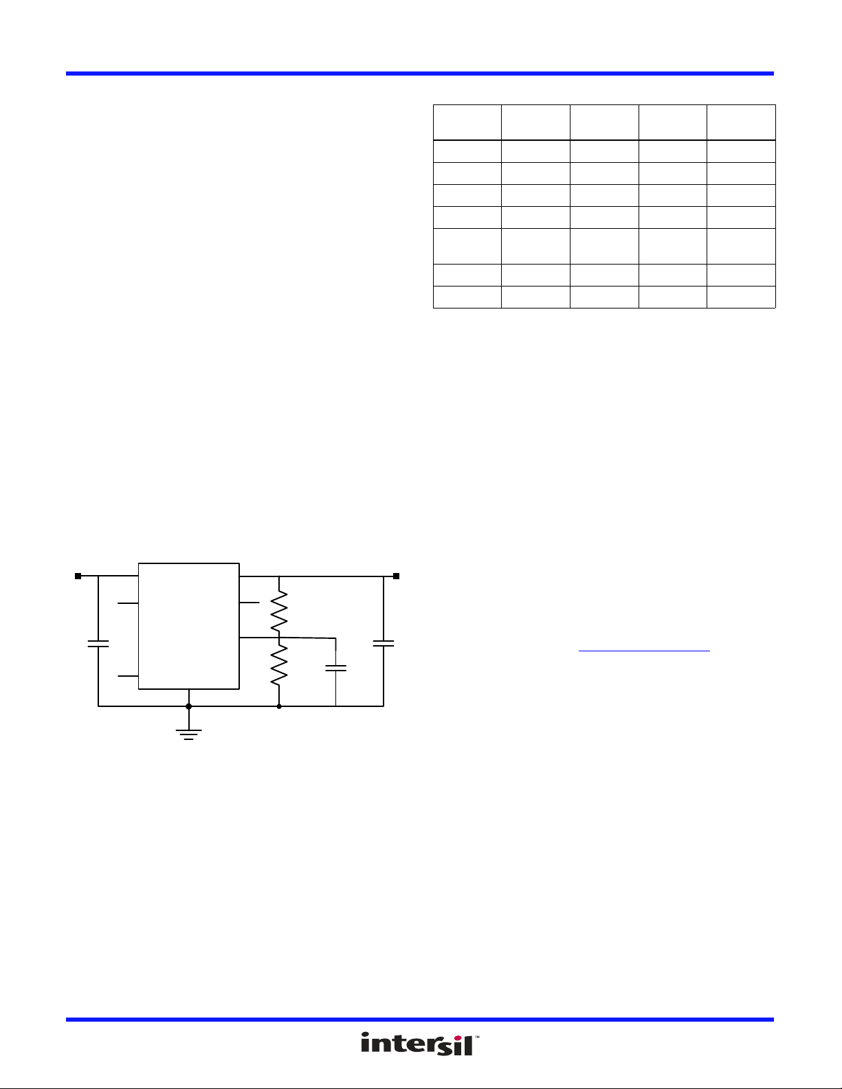
FIGURE 2. ISL75051SRH TYPICAL APPLICATION
ISL75051SRH
CIN
RTOP
RBOTTOM
CP
VIN VOUT
EN
OCP
PG
COUT
ADJ
TABLE 1. RECOMMENDED OUTPUT CAPACITOR VALUES
VOUT
(V)
RTOP
(kΩ)
RBOTTOM
(Ω)
CP
(pF)
COUT
(µF)
5.0 4.32 499 120 220
4.0 4.32 634 120 220
2.5 4.32 1.13k 120 220
1.8 4.32 1.74k 100 220
1.5
(Note 1)
4.32 2.26k 100 47
1.5 4.32 2.26k 100 220
0.8 4.32 7.87k 68 220
NOTE:
1. Either option could be used depending on cost/performance
requirements.


