UG124 Rev.0.00 Page 3 of 9
Jul 24, 2017
ISL70321SEHDEMO1Z 2. Board Functional Description
2. Board Functional Description
The ISL70321SEHDEMO1Z demonstration board provides a simple platform with which to drop in an integrated
circuit solution to sequence up to four events into an existing or a prototype multi power supply system circuit.
After it is connected into the circuit and properly addressed using the UP and INIT inputs, the ISL70321DEMO1Z
starts sequencing the ENABLE outputs from low to high, EN1 through EN4 order. The DONE output is released to
pull high after sequencing is completed.
After the UP input is pulled low, the ISL70321SEHDEMO1Z starts sequencing the ENABLE outputs from high to
low, EN4 through EN1 order. The DONE output is pulled low when the down sequencing is completed.
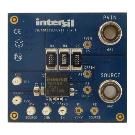
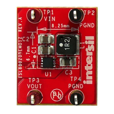
The ISL70321SEHDEMO1Z is shown in Figures 8 through 10 in photographic and schematic forms.
2.1 Operating Range
The ISL70321SEHDEMO1Z is configured for the operating conditions of VDD from 3V to 13.2V, with the ENx
outputs resistively connected to the VCC5 5V pull-up supply. The VMx, UP, and INIT inputs are limited to a
maximum of 5V.
2.2 Default Configuration Settings
All functional and performance configuration settings for this demonstration board will be set by the circuit design
requirements. However, a default set of conditions for the VM input threshold and the delay timing have been
configured for building familiarity with its functions before system integration.
The default configuration is set as follows:
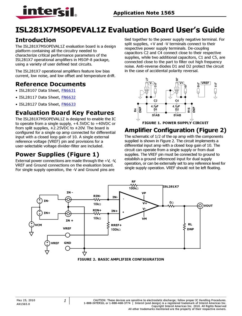
• The VMx inputs all have 2:1 resistor dividers from the VMx_IN connection points to the VM1 to VM4 inputs.
This sets the nominal VM rising input voltage threshold to be ~1.2V.
• The ENx, DONE, and KILL outputs all have 10kΩ pull-up resistors to VCC5.
• The Power-Good Timer (PGTMR) and the Time Delay (TDLY) pins both have 10kΩ resistors to ground
providing a nominal 4ms for the monitored voltage to be ‘GOOD’ and a nominal 2ms for the delay between
sequenced enable outputs.
2.3 Quick Start Guide
With the default or user intended configuration components in place, ensure that the board is properly connected to
the appropriate supplies and loads before applying any power.
(1) Change the delay and power-good timer resistors on the board as necessary to achieve the desired timing of
sequenced events using the provided resistor positions.
(2) Connect the appropriate bias supply to VDD and GND.
(3) Connect the enabling input of the POLs to be sequenced to the appropriate ISL70321SEH ENx outputs in
order of desired turn-on sequence
(4) Connect the POL outputs to the appropriate ISL70321SEH VMx inputs.
(5) Connect UP to the appropriate signaling input.
(6) Use oscilloscopes and DVMs to monitor signals and voltages.
(7) Turn system input power supply ON.
(8) Signal the UP input.
(9) Observe sequencing function and adjust timing and threshold voltages as desired.

