Intrinsyc Open-Q 605 User manual

Intrinsyc Open-Q™ 605 SBC User Guide and HW
Specification
[Document: ITC-01RND1384-UG-001 Version: 1.4]
Your use of this document is subject to and governed by those terms and conditions in the Intrinsyc Purchase an Open-Q™605 Development Kit
based on the Qualcomm QCS605 Processor and Software License Agreement for the Open-Q™ 605 Development Kit, which you or the legal entity
you represent, as the case may be, accepted and agreed to when purchasing an Open-Q™ Development Kit from Intrinsyc Technologies Corporation
(“Agreement”). You may use this document, which shall be considered part of the defined term “Documentation” for purposes of the Agreement,
solely in support of your permitted use of the Open-Q™ 605 Development Kit under the Agreement. Distribution of this document is strictly
prohibited without the express written permission of Intrinsyc Technologies Corporation and its respective licensors, which they can withhold,
condition or delay in its sole discretion.
Intrinsyc is a trademark of Intrinsyc Technologies Corp., registered in Canada and other countries. QUALCOMM and Snapdragon™are trademarks
of QUALCOMM Incorporated, registered in the United States and other countries. Other product and brand names used herein may be trademarks
or registered trademarks of their respective owners.
This document contains technical data that may be subject to U.S. and international export, re-export, or transfer (“export”) laws. Diversion contrary
to U.S. and international law is strictly prohibited.

Intrinsyc Open-Q™ 605 SBC User Guide and HW Specification V. 1.4
2
Copyright Intrinsyc Technologies Corporation
IDENTIFICATION
Document Title Intrinsyc Open-Q™ 605 SBC User Guide and HW Specification
Document Number ITC-01RND1384-UG-001
Version 1.4
Date Nov 26, 2019
History
REVISION
DATE
DESCRIPTION
PAGES
1.0
Jan. 10, 2019
Initial Release
All
1.1
Mar. 8, 2019
Added battery, camera module, and LCD module
information. Added more details on the expansion
connector.
All
1.2
May 1, 2019
Added power consumption numbers
Corrected error in Table 3-3
37
16
1.2.1
July 11, 2019
Corrected error in section 3.5.1 Battery Power to
match Table 3-3. Added clarifications to jumper
settings in sections 3.5.1 and 3.5.2.
16, 17
1.3
Oct. 15, 2019
Updated document to include changes from REV2
hardware
All
1.4
Nov 26, 2019
Updated power consumption Table 4-4 for REV2
hardware.
38

Intrinsyc Open-Q™ 605 SBC User Guide and HW Specification V. 1.4
3
Copyright Intrinsyc Technologies Corporation
Table of Contents
1. INTRODUCTION.................................................................................5
1.1 Purpose........................................................................................................ 5
1.2 Scope...........................................................................................................5
1.3 Intended Audience ...................................................................................... 5
1.4 Acronyms and Abbreviations .....................................................................5
1.5 Signal Name Suffix.....................................................................................6
2. REFERENCE DOCUMENTS................................................................7
2.1 Applicable Documents................................................................................7
2.2 Reference Documents.................................................................................7
2.3 List of Figures.............................................................................................8
2.4 List of Tables ..............................................................................................9
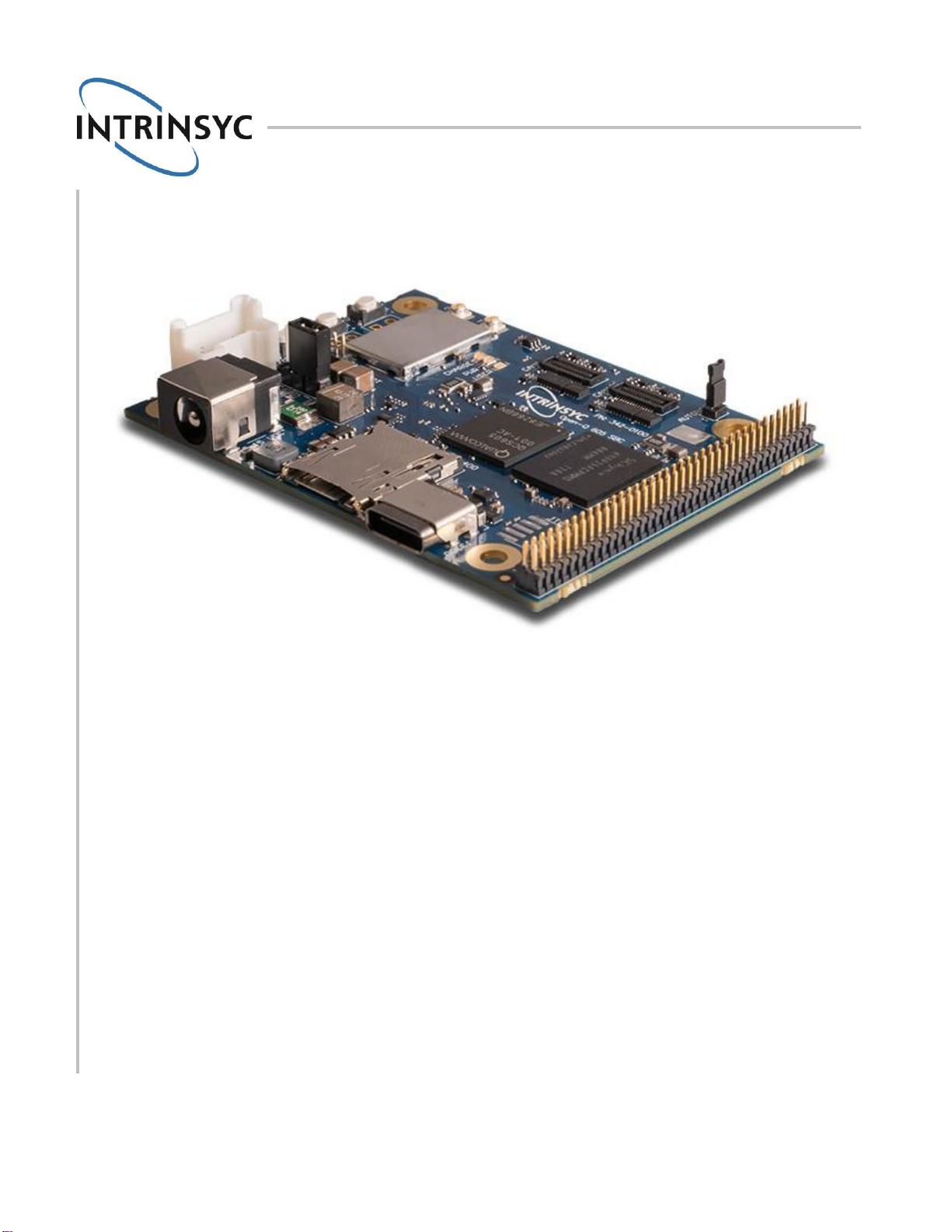
3. OPEN-Q™ 605 SBC OVERVIEW.......................................................10
3.1 Open-Q™ 605 SBC System Specifications..............................................12
3.2 Handling Precautions................................................................................13
3.2.1 ESD Precautions......................................................................................................13
3.2.2 Storage.....................................................................................................................13
3.3 Kit Contents..............................................................................................13
3.4 Getting Started ..........................................................................................14
3.4.1 Registration .............................................................................................................14
3.4.2 How to Connect a Debug UART.............................................................................15
3.5 Powering Up the SBC...............................................................................16
3.5.1 Battery Power..........................................................................................................16
3.5.2 DC Power ................................................................................................................18
3.6 SBC Connectors........................................................................................19
3.7 DC Power Input (J3500)...........................................................................20
3.8 Battery Connector (J3502)........................................................................21
3.9 Open-Q™ 605 Display Connector (J2700) ..............................................22
3.10 Camera Connectors (J2500, J2501)..........................................................23
3.11 Expansion Connector (J3600)...................................................................26
3.12 External Wi-Fi/BT Antenna Port Specification (J3000, J3001)...............34
3.13 External GPS Antenna (J3100).................................................................34
3.14 Micro SD Card (J2400).............................................................................35
3.15 USB Type C Connector (J3300)...............................................................35
4. ELECTRICAL SPECIFICATIONS.....................................................37
4.1 Absolute Maximum Ratings ..................................................................... 37
4.2 Recommended Operating Conditions.......................................................37
4.3 Operating Temperature.............................................................................38
4.4 Power Consumption..................................................................................38
5. MECHANICAL SPECIFICATIONS ...................................................39
5.1 Introduction...............................................................................................39
5.2 Location of Major Components................................................................39

Intrinsyc Open-Q™ 605 SBC User Guide and HW Specification V. 1.4
4
Copyright Intrinsyc Technologies Corporation
5.2.1 Top Side ..................................................................................................................39
5.2.2 Bottom Side.............................................................................................................39
5.3 SBC Mechanical Outline ..........................................................................41
5.4 Top and Bottom Height Restrictions ........................................................41
5.5 Weight.......................................................................................................41
5.6 Labeling Information ................................................................................42
6. ACCESSORIES FOR THE 605 SBC....................................................43
6.1 Camera Module.........................................................................................43
6.2 LCD Display Accessory ...........................................................................46
7. PACKAGING AND SHIPPING INFORMATION ...............................49
8. RADIO CERTIFICATION INFORMATION ......................................50
9. ROHS / REACH COMPLIANCE ........................................................51
10. COMPANY CONTACT ......................................................................52

Intrinsyc Open-Q™ 605 SBC User Guide and HW Specification V. 1.4
5
Copyright Intrinsyc Technologies Corporation
1. INTRODUCTION
This document applies to the Intrinsyc Open-Q™ 605 SBC.
1.1 Purpose
The purpose of this document is to provide primary technical information and describe the
features, functionality, and electrical and mechanical specifications of the Intrinsyc Open-Q™
605 SBC. In addition, this document will also provide a brief GPIO/BLSP programming guide.
1.2 Scope
This document describes the features, functionality, and electrical and mechanical specifications
of the Intrinsyc Open-Q™ 605 SBC. In addition to that, the document will also cover the
following items:
•Design guide for interfacing the included expansion interfaces
1.3 Intended Audience
This document is intended for users evaluating or designing products with the Intrinsyc Open-
Q™ 605 SBC.
1.4 Acronyms and Abbreviations
Acronym / Abbreviation
Definition
ANT
ANTenna
BOM
Bill Of Materials
BSP
Board Support Package
BT
BlueTooth
CLK
Clock
CPU
Central Processing Unit
CS
Chip Select
CSI
Camera Serial Interface
DSI
Display Serial Interface
DNP
Do Not Populate
EMI
Electro-Magnetic Interference
EN
ENable
ERM
Eccentric Rotating Mass
ESD
Electro-Static Discharge
FPC
Flexible Printed Circuit
GND
GrouND
GPIO
General Purpose I/O
GPS
Global Positioning System
HDMI
High Definition Multimedia Interface
I2C
Inter-Integrated Circuit
I2S
Inter-IC Sound
INT
INTerrupt
JTAG
Joint Test Action Group
LDO
Low Drop-Out
LNA
Low Noise Amplifier
LRM
Linear Resonant Actuator
LTE
Long-Term Evolution

Intrinsyc Open-Q™ 605 SBC User Guide and HW Specification V. 1.4
6
Copyright Intrinsyc Technologies Corporation
MDP
Mobile Display Port
MI2S
Mobile Inter-IC Sound
MIC
MICrophone
MIPI
Mobile Industry Processor Interface
MPP
Multi-Purpose Pin
NFC
Near Field Communication
PCB
Printed Circuit Board
PCIE
Peripheral Component Interconnect Express
PWM
Pulse-Width Modulation
RF
Radio Frequency
RX
Receive
SCL
Serial CLock
SDA
Serial DAta
SDC
Secure Digital Interface
SBC
Single Board Computer
SMPS
Switch-mode Power Supply
SPI
Serial Peripheral Interface
SSC
Snapdragon™ Sensor Core
TX
Transmit
UART
Universal Asynchronous Receiver/Transmitter
UIM
User Interface Module
USB
Universal Serial Bus
WLAN
Wireless Local Area Network
1.5 Signal Name Suffix
Suffix
Definition
_N
Indicates that the signal is ACTIVE LOW
_P/N
Identifies the two signals comprising a differential pair

Intrinsyc Open-Q™ 605 SBC User Guide and HW Specification V. 1.4
7
Copyright Intrinsyc Technologies Corporation
2. REFERENCE DOCUMENTS
This section lists any parent and supplementary documents for the Open-Q™ 605 SBC. Unless
stated otherwise, applicable documents supersede this document and reference documents
provide background and supplementary information.
2.1 Applicable Documents
REFERENCE
AUTHOR
TITLE
A-1
Intrinsyc
Intrinsyc Purchase and Software License Agreement
for the Open-Q™ 605 SBC
2.2 Reference Documents
These documents are available to registered customers on the Intrinsyc support site:
https://tech.intrinsyc.com
REFERENCE
TITLE
R-1
Open-Q™ 605 SBC Schematics
R-2
Open-Q™ 605 SBC Bill of Materials
R-3
Open-Q™ 605 SBC BSP Software Release Notes
R-4
Open-Q™ 605 SBC HW Revision Guide

Intrinsyc Open-Q™ 605 SBC User Guide and HW Specification V. 1.4
8
Copyright Intrinsyc Technologies Corporation
2.3 List of Figures
Figure 1: Open-Q™ 605 SBC block diagram ................................................................................11
Figure 2: Open-Q™ 605 SBC label located at the bottom side of the SBC ..................................14
Figure 3: Debug UART pin locations............................................................................................15
Figure 4: J3501 pin configuration for battery power .....................................................................17
Figure 5: Battery Connector (J3502)..............................................................................................17
Figure 6: J3501 pin configuration for DC power...........................................................................19
Figure 7: DC jack (J3500)..............................................................................................................20
Figure 8: Battery connector (J3502)...............................................................................................21
Figure 9: 30-Pin display connector (J2700)...................................................................................22
Figure 10: Camera connectors (J2500 and J2501, from left to right)............................................23
Figure 11: 76-Pins expansion connector (J3600)..........................................................................26
Figure 12: WLAN/BT antenna connectors (J3000/J3001) ............................................................34
Figure 13: GPS Antenna Connector (J3100)..................................................................................34
Figure 14: micro SD card port (J2400) ..........................................................................................35
Figure 15: USB Type-C Connector (J3300) ..................................................................................35
Figure 16: Open-Q™ 605 SBC (top view) ....................................................................................39
Figure 17: Open-Q™ 605 SBC (bottom view) with pin 1 locations..............................................40
Figure 18: SBC mechanical outline (top view)..............................................................................41
Figure 19: Open-Q™ 605 SBC Label............................................................................................42
Figure 20: Two Versions of IMX258 Module...............................................................................43
Figure 21: CAM0 (Red) and CAM2 (Yellow) location.................................................................43
Figure 22: Camera module Pin 2 location......................................................................................44
Figure 23: Camera module aligned to CAM0 connector...............................................................44
Figure 24: Camera module aligned to CAM2 connector...............................................................44
Figure 25: Camera module connected to CAM0 connector...........................................................45
Figure 26: Camera module connected to CAM2 connector...........................................................45
Figure 27: 605 SBC LCD/Touchscreen.........................................................................................46
Figure 28: J2700 (latch in closed position)....................................................................................46
Figure 29: Display connector (latch opened).................................................................................47
Figure 30: Display cable inserted (latch opened)...........................................................................47
Figure 31: Cable attached to the display connector .......................................................................48
Figure 32 - Individual SBC Packaging ..........................................................................................49
Figure 33 –Packaging for Large Quantity Shipments...................................................................49

Intrinsyc Open-Q™ 605 SBC User Guide and HW Specification V. 1.4
9
Copyright Intrinsyc Technologies Corporation
2.4 List of Tables
Table 3-1 - Open-Q™ 605 SBC functional specifications.............................................................12
Table 3-2 –Debug UART connection ...........................................................................................15
Table 3-3 –Jumper settings for DC or battery power input...........................................................16
Table 3-4 –Jumper settings for different boot options..................................................................16
Table 3-5 –Open-Q™ 605 SBC Absolute Maximum Input Power Rating...................................18
Table 3-6 –Open-Q™ 605 SBC Operating Conditions.................................................................18
Table 3-7 –SBC expansion options and usage..............................................................................19
Table 3-8 –Battery connector J3502 pin out.................................................................................22
Table 3-9 –Display connector J2700 pin out ................................................................................22
Table 3-10 –Camera 0 connector J2500 pin out ...........................................................................24
Table 3-11 –Camera 1 connector J2501 pin out ...........................................................................24
Table 3-12 –Open-Q™ 605 SBC expansion connector J3600 pin out .........................................26
Table 3-13 –Summary of GPIOs...................................................................................................28
Table 3-14 –Summary of LPI_GPIOs...........................................................................................30
Table 3-15 –Summary of Audio Related Signals..........................................................................32
Table 3-16 –Summary of System Control Signals........................................................................32
Table 3-17 –Summary of User Interface Signals..........................................................................33
Table 3-18 –Summary of Power Rails..........................................................................................33
Table 3-19 –WLAN/BT antenna connector details.......................................................................34
Table 3-20 –GPS antenna connector details .................................................................................35
Table 4-1 - Absolute maximum input voltage rating.....................................................................37
Table 4-2 - Recommended input voltage range.............................................................................37
Table 4-3 - Operating temperature range (Tc) ...............................................................................38
Table 4-4 - Power consumption for different operational modes ..................................................38
Table 5-1 –Intrinsyc product label format.....................................................................................42

Intrinsyc Open-Q™ 605 SBC User Guide and HW Specification V. 1.4
10
Copyright Intrinsyc Technologies Corporation
3. OPEN-Q™ 605 SBC OVERVIEW
The Open-Q™ 605 SBC is a 50mm x 68mm production-ready, computing platform powered by
the Qualcomm QCS605 system-on-chip.
Figure 1, below, shows the block diagram of the SBC and this section describes the system
features of the SBC. Note that some of the components and functionality may not be included in
some versions of the SBC and some functionality may not be supported by certain software
versions. Please see Release Notes (R-3) for details on what is supported by the Board Support
Package SW.

Intrinsyc Open-Q™ 605 SBC User Guide and HW Specification V. 1.4
11
Copyright Intrinsyc Technologies Corporation
Figure 1: Open-Q™ 605 SBC block diagram

Intrinsyc Open-Q™ 605 SBC User Guide and HW Specification V. 1.4
12
Copyright Intrinsyc Technologies Corporation
3.1 Open-Q™ 605 SBC System Specifications
The Open-Q™ 605 SBC platform encompasses the following hardware features:
Table 3-1 - Open-Q™ 605 SBC functional specifications
Subsystem /
Connectors
Feature Set
Description
Specification
Processor
QCS605
Qualcomm Technologies Inc. (QTI)
processor for visual intelligent platform
applications
Octa-core Kryo 300 (1MB
L3 cache)
2x: Gold (2.5 GHz, 256
KB L2 cache)
6x: Silver (1.7GHz, 128
KB L2 cache)
Qualcomm Adreno
GPU 615
High Performance 3D Graphics
Accelerator
64-bit addressing,
780MHz
Qualcomm
Hexagon DSP
Dual Hexagon DSP Vector eXtensions
(HVX)
1.2GHz
Memory
Support
4GB LPDDR4X
Memory
Designed for a 1866 MHz
clock supported via
2x16bit EBI
256 KB/512KB
IMEM/GMEM for graphics
32GB eMMC
Primary Storage for platform. Used for
storing software applications and user data
SD 3.0
Power
Management
Qualcomm PM670
+ PM670L
PM670+PM670L: Integrated switching
charger with Qualcomm Quick Charge
technology 4.0, 38.4 MHz system clock
generation
PM670L: LCD support, integrated audio
codec, 5 switching regulators and 10
LDOs
Wireless
WLAN 802.11
a/b/g/n/ac,
BLE 5.x
WCN3990 WIFI, BT, and FM combo
SDIO v3.0 interface,
Support of BLE 5.x, 2x2
multiple input, multiple
output (MIMO)
Location
Qualcomm
SDR660G GNSS
Receiver
GPS, GLONASS, Galileo, and BeiDou
support
Connectivity
USB 3.1
Can support Type-C with DisplayPort
UART
1 dedicated 2 wire, 1 assignable 2 wire, 1
assignable 4 wire
SDC
4 lane SDIO for SD card
Audio
PM670L
Integrated PMIC audio codec

Intrinsyc Open-Q™ 605 SBC User Guide and HW Specification V. 1.4
13
Copyright Intrinsyc Technologies Corporation
Subsystem /
Connectors
Feature Set
Description
Specification
Multimedia
Interfaces
MIPI CSI
Two 4-lane CSI interfaces(CSI0 and
CSI2)
D-PHY: 2.5 Gbps per lane
C-PHY: ~17 Gbps (2.5 G
symbols per trio per
second)
MIPI DSI
One 4-lane DSI interfaces (DSI0)
D-PHY 1.2; C-PHY 1.0;
VESA DSC 1.1.
Mobile display
processor
Snapdragon™ Display Engine 775 for
display processing
Video Encoder and
Decoder
5.7K30/4K60 8-bit:
HEVC/H.264 + 1080p60
Configurable
GPIO
GPIO
32 GPIOs: programmable as pull-up, pull-
down, keeper, or no pull, programmable
drive current, Top-level mode multiplexer
for GPIO group control
PLL and
Clocks
Clock input
19.2 MHz CXO clock input
3.2 Handling Precautions
3.2.1 ESD Precautions
Electrostatic discharge (ESD) occurs naturally in laboratory and factory environments. An
established high-voltage potential is always at risk of discharging to a lower potential. If this
discharge path is through a semiconductor device, destructive damage may result.
The SBC has ESD protection only on the interfaces meant to be externally accessible in a
product, therefore, it should be handled only in a static-safe environment when not installed in an
enclosure. When using the SBC as an exposed board, proper anti-static precautions should be
employed, including but not limited to:
•Using a grounded anti-static mat
•Using a grounded wrist or foot strap
3.2.2 Storage
The SBC should be stored in an anti-static bag and not exposed to high humidity.
3.3 Kit Contents
The Open-Q™ 605 SBC Development Kit includes the following:
•Open-Q™ 605 SBC with the Snapdragon™QCS605 processor
•AC Power Adapter
•2 Wi-Fi/BT antennas
•Quick Start Guide

Intrinsyc Open-Q™ 605 SBC User Guide and HW Specification V. 1.4
14
Copyright Intrinsyc Technologies Corporation
3.4 Getting Started
This section explains how to setup the Open-Q™ 605 SBC and start using it.
3.4.1 Registration
To register the development kit and gain access to the Intrinsyc support site, please visit:
http://tech.intrinsyc.com/account/register .
To proceed with registration, the development kit serial number is required. The serial number
can be found on the label on the bottom side of the SBC. The label contains the Serial Number
and WIFI MAC address.
Note: Please retain the SBC serial number for warranty purposes.
Refer to http://tech.intrinsyc.com/account/serialnumber for more details about locating the
development kit serial number.
Figure 2: Open-Q™ 605 SBC label located at the bottom side of the SBC

Intrinsyc Open-Q™ 605 SBC User Guide and HW Specification V. 1.4
15
Copyright Intrinsyc Technologies Corporation
3.4.2 How to Connect a Debug UART
The debug UART port on the Open-Q™ 605 SBC can be found on the Expansion Connector
(J3600) (for Expansion Connector pinout information, please refer to section 3.11). To access the
debug UART, follow the pinouts in Table 3-2 below. Note that the UART interface voltage level
is 1.8V.
It is recommended to use a serial-USB adapter cable such as the TTL-232RG-VREG1V8-WE
from FTDI. Available here:
https://www.digikey.ca/product-detail/en/ftdi-future-technology-devices-international-ltd/TTL-232RG-VREG1V8-
WE/768-1070-ND/2441359
Table 3-2 –Debug UART connection
Pins
Signal Name
Interface Voltage Level
71
QUP12_DBG_UART_TX
1.8V
73
QUP12_DBG_UART_RX
1.8V
75
GND
GND
Figure 3: Debug UART pin locations
Pin 1
Pin 71
Pin 73
Pin 75

Intrinsyc Open-Q™ 605 SBC User Guide and HW Specification V. 1.4
16
Copyright Intrinsyc Technologies Corporation
3.5 Powering Up the SBC
To power up the Open-Q™ 605 SBC, jumper settings and boot configurations need to be set
correctly. As part of the design, the system can be powered by either a battery or by DC power.
Please see Table 3-3 and Table 3-4 for correct jumper settings and boot option configurations.
Table 3-3 –Jumper settings for DC or battery power input
Power Input
Jumper J3501
Jumper J3503
Jumper J3504
DC Power
Short pins 1 and 2
Short pins 1 and 2
Short pins 1 and 2
Battery Power
Short pins 2 and 3
Open
Open
Note: Please ensure jumper settings are set accordingly prior to powering up the system to
prevent back charging the on board power supply circuitry.
Apart from the input power source, different boot configurations can be set on the Open-Q™ 605
SBC. Table 3-4 refers to the various jumper settings that are available for different boot options.
Please note that the only boot from eMMC is supported by current BSP. Please contact Intrinsyc
to enable different boot options such as boot from USB or SD card.
Table 3-4 –Jumper settings for different boot options
Boot Configuration
J3403
J3404
Notes
Boot by key event (pressing power ON key S3400)
Open
Open
Autoboot upon DC power input
Open
Short
Qualcomm Download Mode
Short
Open
Not supported in current BSP
3.5.1 Battery Power
To power the Open-Q™ 605 SBC development kit with a battery, the following settings must be
followed. As seen in the figure below, set the following jumpers to:
•J3504 (“ID”): No jumper installed –charging enabled
•J3503 (“THERM”) : No jumper installed –connected to thermistor in battery pack
•J3501: Install 2 pin jumper on pins 2 and 3 (“BATT” side)

Intrinsyc Open-Q™ 605 SBC User Guide and HW Specification V. 1.4
17
Copyright Intrinsyc Technologies Corporation
Figure 4: J3501 pin configuration for battery power
After connecting pin jumpers on the locations above, connect a battery to the battery header
(J3502). Detail mechanical information of the connector is provided in Section 3.8.
Figure 5: Battery Connector (J3502)
3.5.1.1 Battery Pack Selection
Intrinsyc does not sell nor ship battery packs with the Open-Q™ 605 SBC Development
Kit. Users sourcing their own battery pack should note the absolute and operating input
power ratings of the SBC listed below.

Intrinsyc Open-Q™ 605 SBC User Guide and HW Specification V. 1.4
18
Copyright Intrinsyc Technologies Corporation
Table 3-5 –Open-Q™ 605 SBC Absolute Maximum Input Power Rating
Parameter
Min
Max
Units
Battery power input (VBATT)
-0.5
6 (Steady State)
7 (Transient, <10msec)
V
5V USB VBUS battery charger input voltage source (USB_VBUS)
-0.3
16
V
Table 3-6 –Open-Q™ 605 SBC Operating Conditions
Parameter
Min
Typ.
Max
Units
Battery power input (VBATT)
3.451
3.8
4.75
V
5V USB VBUS battery charger input voltage source (USB_VBUS)
3.6
5
10
V
Intrinsyc recommends using the AA Portable Power Corp’s CU-J479-V2 / 1ICP7/55/85
Lithium ion battery pack. This is a single cell pack with a nominal voltage of 3.8V and a
capacity of 3200mAh (11.8Wh, 5A rate) with a thermistor included in the battery pack.
When using this battery, the default battery receptacle needs to be replaced such that it
can mate with the battery header on the SBC (J3502). Please refer to Section 3.8 for
connector information.
3.5.2 DC Power
To power the Open-Q™ 605 SBC development kit with an external DC source, set the following
jumpers, as seen in the figure below:
•J3504 (“ID”): Install 2-pin jumper –to disable charging
•J3503 (“THERM”): Install 2-pin jumper –to connect dummy thermistor resistor
•J3501: Install 2 pin jumper on pins 1 and 2 (“DC”, side)
1
The SBC may be configured to operate at voltage levels lower than the minimum listed. Changes to default
software settings are required. For battery operation at lower voltages, additional considerations should be taken as to
the effects on battery life-cycle.

Intrinsyc Open-Q™ 605 SBC User Guide and HW Specification V. 1.4
19
Copyright Intrinsyc Technologies Corporation
Figure 6: J3501 pin configuration for DC power
Connect the supplied 12 VDC adaptor to DC Jack (J3500). Alternatively, DC power (5-15V) may
be connected to the Expansion Connector. See section 3.11 for the Expansion Connector pinout
table.
3.6 SBC Connectors
The following table provides an overview of the connectors, expansions, and their usages on the
SBC.
Table 3-7 –SBC expansion options and usage
Domain
Description
Specification
Usage
Power
AC/barrel connector
12 V DC Power Supply
5A current
DC power input
Battery Connector
4 pin header
For battery operation and
charging
Buttons
Power button
SMD button
Button for power on/off
and suspend/resume
Volume + key
SMD Button
Volume +Key
Volume –key
SMD Button
Volume –Key
LCD Display and
Touch connector
30 pin for LCD signals via
FPC connector to display
adapter board
4-lane MIPI DSI0
I2C/SPI/GPIO
Backlight
MIPI Alliance Specification
v1.01
MIPI D-PHY Specification
v0.65,v0.81, v0.90, v1.01
To drive MIPI DSI LCD
panel with touch controller
CSI Camera
connectors
2 x CSI port connector with
CLK, GPIOS, CCI
Supports 2 x Camera
interfaces via two separate
connectors
•2 x MIPI-CSI each 4
lane
•Separate I2C / CCI
control
To connect third party
camera module

Intrinsyc Open-Q™ 605 SBC User Guide and HW Specification V. 1.4
20
Copyright Intrinsyc Technologies Corporation
Domain
Description
Specification
Usage
MIPI Alliance Specification
v1.00 for Camera Serial
Interface
Expansion
connector
External GPIO connections
76 pin GPIO/power header
For connecting external
peripherals
WLAN Antenna
2x U.FL connector
2.4 –5.1 GHz
To connect off board PCB
antenna via U.FL
connector
GPS Antenna
1x U.FL connector
GPS :
1574.42 MHz –1576.42 MHz
GLONASS :
1587 MHz –1606 MHz
BDS B1:
1559.1 MHz –1563.1 MHz
Galileo:
1573.4 –1577.5 MHz
To connect off board PCB
antenna via U.FL
connector
Micro SD
Micro SD card
4bit Micro SD card support
External Storage
USB 3.1 (Type-
C)
Native USB 3.1 from
QCS605
USB Type C connector
USB device (ADB) and
host mode (OTG)
The following sections below will provide in-depth information on each expansion header and
connector on the SBC. The information listed below is of particular use for those who want to
connect other external peripherals on the Open-Q™ 605 SBC. To prevent hardware damage,
please ensure peripherals meet the electrical specifications of the system before connecting
anything to the SBC.
3.7 DC Power Input (J3500)
The Open-Q™ 605 SBC DC power source connects to the 12V DC power supply jack J3500.
Starting from the power jack, the 12V power supply branches off into a synchronous step-down
converter (U3500) that directs to the PMIC PM670’s charger (see Open-Q™ 605 SBC
Schematics, R1).
Figure 7: DC jack (J3500)
The SBC consists of 2 PMIC modules. Functionalities of the 2 modules are outlined below:
Table of contents
Other Intrinsyc Motherboard manuals
Popular Motherboard manuals by other brands

Biostar
Biostar P4 TDG Engineering validation test report

NXP Semiconductors
NXP Semiconductors FRDM-KW38 quick start guide

MSI
MSI K9N6PGM-F - Motherboard - Micro ATX user guide

Biostar
Biostar I91PL-A7 PCI-ED user manual

STMicroelectronics
STMicroelectronics STM32L152D-EVAL user manual

Atmel
Atmel SAM4N Xplained Pro user guide