JBL EON15 G2 Operating manual

Technical Service Manual
Rev. A
7/16/2004

TABLE OF CONTENTS
PRODUCT OVERVIEW 3
SPECIFICATIONS/FREQUENCY RESPONSE GRAPHIC 4
PANEL CONTROLS, CONNECTORS AND INDICATORS 5
BLOCK DIAGRAM 8
CIRCUIT DESCRIPTIONS 9
TROUBLESHOOTING GUIDE 18
SEMICONDUCTOR DIAGRAMS 21
FINAL TEST PROCEDURE 22
PICTORIALS OF PCB ASSEMBLIES 23
JBL WARRANTY LIMITED WARRANTY 26 - 65
SYSTEM EXPLODED VIEW
FAILURE QA CODES
SCHEMATICS / MASTER PARTS LIST

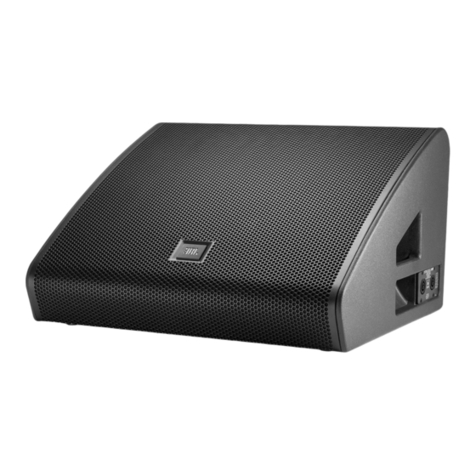
Product Overview

Specifications
Frequency Response
Notes:
JBL Professional is continually engaged in research activities to enable further product improvement. New materials, production methods and design
refinements are instituted into the existing product without notification and, therefore, the information contained within this manual is subject to
change without notice. Rest assured that your JBL Professional equipment will always equal or exceed the published design specifications unless
otherwise stated.

Connectors, Controls and Indicator


EON15 G2 Block Diagram

AC Input Module
The main line voltage is connected at input jack P1 on the ac input PCB. Capacitors C2 and C3 work
in conjunction with C1 to help reduce the instantaneous line voltage spikes that cause static noise in
the high frequency range. Pin 2, the AC ground, is connected to chassis ground. Pins 1 and 3 are
connected to the 2-pole 2-position main power switch, SW1. Toggling of SW1 directs the ac voltage to
travel through fuses, F1 and F2, to the voltage selector switch, SW2 that allows the customer to
manually select between 120V or 230V. It is important to power down the equipment before this
switch is operated to avoid possible driver damage. Electrically, this switch, SW2, determines which
power transformer primary receives the applied alternating current so that the proper output voltage
will result.
We will assume that the mains input voltage to the transformer is 115 Vac for this circuit description.
The toroidal transformer output would then deliver 60Vac to the power supply connector P3 on the
main amplifier PCB.

Power Supply
Initially, raw alternating current enters the EON15-G2 from the IEC connector on the AC input PCB and is
directly connected to the power switch SW1 through the main fuses F1 & F2. Toggling SW2 directs the ac
voltage to travel to the voltage selector switch that allows the customer to select between 120V or 230V.
Electrically, this switch determines which power transformer primary is applied so that the proper output voltage
will result. In either case, the voltage will be stepped down by the toroidal transformer windings.
The toroidal transformer steps down the input alternating voltage from 120Vac to 60Vac and enters the main
PCB at P3, where it is rectified into ±40Vdc by bridge rectifier BR1. It is filtered by capacitors C75 and C76 . .
. the end result is a stable power supply. This voltage is used for the rails for the low and high frequency power
amplifiers, which provides a full signal voltage swing from peak to peak of 80 volts.
Simultaneously, this rectified voltage from BR1 is also passed through clamping diodes D9 and D10 and
regulated at ±15 Vdc by Q15 and Q16, respectively. This low voltage power supply drives the signal processing
IC’s and housekeeping/fault detection circuitry.
Voltage doubling circuitry supplies the ±80 Vdc necessary to supply the drivers and pre-drivers. By utilizing
this bootstrap configuration, the adjacent stages are prevented from scavenging the voltage from the rails during
demanding informational or musical passages.
The LED DS2 is used as a pilot lamp.
Delay is provided on initial power up by the time constant of C46 and R77. Once charge builds up at C46, Q14
biases off after 4 seconds allowing comparator U5C to toggle taking its output high. Directly connected to Q6
and Q1 this action enables both amplifiers. Upon power down, Q14 is instantaneously biased on causing the
toggling of U5C, thereby, disabling both amplifiers until C46 is totally discharged via R93 and R98.
Excessive heatsink temperature will cause RT1 to short, toggling U5C, and enabling amplifier shutdown.

Loop/Mix Input Circuitry
Shown above is the Input Loop/ Mixture Circuitry with the accompanying Channel 2 and 3 Input and
Equalization Circuits for the EON 15-G2. NOTE: It is assumed that the technician is familiar with the
main XLR input circuit for this discussion.
Balanced input signal enters the ¼” connectors at J3 and J4 for auxiliary input channel’s 2 and 3 and is
isolated by IC’s U4-A and U4-B. The corresponding output signals traverse pins 2 and 3 of RC2 to the
individual volume controls VR3 and VR2. At this point, all input signals (including the XLR input
signal at pin 1 of RC2 from pin 7 of U5-B from input PCB) are summed at the non-inverting input of
U1A on the EQ PCB. The resulting signal is output on pin 1 and is directly connected to the boost side
of the equalization controls. A 12-dB cut or boost in signal can be achieved by this equalization
amplifier which begins at the non-inverting input pin 6 of U1-B. This output signal is returned to the
Input PCB via pin 7 of RC2 and is separated into two signal paths by isolation IC’s U2-A and U2-B.
The desired output signal is determined by toggling the 3-pole, 2-throw switch SW1 between the
original “pure” input signal and an equalized “mixture” of that input signal. This allows the user to
loop or daisy chain additional sound reinforcement equipment utilizing either signal.
IC’s U3-A and U3-B provide further isolation from the loop/mix circuitry and J1 sending this
“mixture” output signal to the main amplifier PCB via pin 1 of WH1.

Signal Input Circuitry
Voltage measurements are at frequency of 100 Hz with –20 dB on input at XLR (J2).
Balanced input is connected to J2 and travels to impedance selector switch SW2. This switch inserts
R33, R52 and R45 for line level inputs and removes same for microphone level inputs. It also shorts
the “mic” indicator LED (allowing the illumination of the “signal” LED) and changes the gain of
summing amplifier IC U5B. D1 and D2 add input circuitry protection if the input signal is in excess
of ±15Vdc. The signal travels to pins 2 and 3 of buffer amplifier U5A where the Common mode
rejection cleans up the extraneous noise from being amplified.
The signal is output on pin 1 of U5 to the control PCB via connectors RC1/PA1 so the user can adjust
to the desired level using volume control VR1. The signal is returned to the input PCB through
RC1/PA1 and is input to pins 5 and 6 of U5B. This output on pin 7 of .4Vpp, branches into the
mic/signal mode LED indication circuitry (comparator U6), and the equalization circuitry on pin 1 of
RC2.

Signal Peak LED Circuitry
This is the signal indication circuitry for the EON15-G2 that is located on the signal input PCB. The
presence of signal, the peak input signal and/or instantaneous signal overmodulation from both the
high frequency and low frequency amplifiers is shown.
Indication consists of voltage network of LED diodes, DS1, DS2, and DS3 connected in series with
each internal node encompassing IC detection circuitry. Any voltage from the low frequency
amplifier or the high frequency amplifier that is above the voltage drop of D1 or D2 (located on main
PCB) will toggle U6C. This, in turn, will toggle U6D and forward bias the “peak” LED (DS3) emitting
light. Similarly, the “line” or “mic” mode is determined by the position of SW2 (not shown—see input
circuitry description). U6A (not shown) to toggles and U6B (not shown) toggles when multi-switch
SW2 is in the “mic” position thereby illuminating the LED.

High Frequency Signal Processing
Voltage measurements are at frequency of 10Khz with –25dB on input at XLR (not shown).
Shown above is the high frequency signal processing circuitry for the EON 15-GII. Input audio signal
is transferred from the input PCB to the Main Amplifier PCB via multi-pin connector cable. .
Specifically, pin 1 of WH1 carries this signal to pin 1 of connector P1.
A signal of .65Vpp enters the serially connected multipath high pass filters U2-A and U2-B.
U2-D enhances the very high frequencies (midpoint 19khz) while U2-C enhances the lower
frequencies of the high frequency spectrum (midpoint 3Khz). Both these outputs are summed and
amplified at the inverting input of U3-A with an output voltage of 3Vpp which is connected to the high
frequency main amplifier IC U1.

High Frequency Amplifier
Voltage measurements are at frequency of 10Khz with –25dB on input at XLR (not shown).
This is the high frequency power amplifier used in the EON15-G2 after serial number 27225. It uses a
TDA7293 operational power amplifier in a non-inverting configuration with the normal peripheral
components to provide proper equalization and operation. The nominal operating voltage of ±40Vdc is
applied to the IC via pins 7,13 and pins 8,15.
The negative feedback resistor, R8, in conjunction with R7 determine the amplifier’s closed-loop gain.
Signal output from pin 1 of U3A is capacitively coupled by C1 and serially reduced by R1 and
connected to the non-inverting input of U1 at pin 3. Operating stability is increased by adding the
supersonic frequency input filter through the shunt of R7 and C2 and by adding filter C14 and R29 on
the output. These circuits dampen possible resonant oscillations.
Peak output/dc offset voltage from the IC output pin 14 travels to D1 and traverses through connector
P1 is detected at U6 pin 9 on the Signal Input PCB.
The EON15G-2 has thorough IC thermal protection/muting circuitry. Comparator U5 (located on
power supply description) toggles if sensor RT1 (on same) detects a heatsink temperature in excess of
≥60°C. or Q14 (on same) detects a loss of ac power. This resultant shutdown signal is sent to bias Q1
into conduction, which, ultimately, mutes the amplifier preventing possible driver damage.

Low Frequency Signal Processing
Voltage measurements are at frequency of 100 Hz with –20 dB on input at XLR (not shown).
Shown above is the low frequency signal processing circuitry for the EON 15-G2. Signal of .7Vpp
enters from pin 1 of P1 to the serially connected low pass filters U4-A and U4-B. The signal diverges
to U4-C and U4-D where the upper limit (midpoint 110.7Hz) and the lower limit (midpoint 62.2 Hz)
are enhanced and summed by U3-D. This processed signal is output from U3-D and is amplified by
U3-C from .7Vpp to .95Vpp subject to limiting from the negative feedback loop consisting of U5 and
Q2.

LF Amplifier Stage
All Voltage measured with reference to audio ground with no input signal
The low frequency amplifier uses discrete components configured in a push-pull drive
architecture operating in the class AB region and have a measurable gain of 18.52 dB.
The voltage rails for the power amplifier are ±40 Vdc as rectified by bridge BR1 located in the Power
Supply Module. The output and driver transistors are driven by the preceding stages, which make use
of the bootstrap supply voltage of ±80Vdc.
The low frequency processed signal from pin 8 of U3-C enters the differential amplifier consisting of
Q4 and Q5 subject shutdown from Q6.
Physically attached to the heatsink, Q13 dynamically controls the bias for the output transistors and is
statically adjusted at VR1.

TROUBLESHOOTING GUIDE
Any successful electronic repair is dependent upon accurately diagnosing the symptoms that indicate
faulty circuitry to the root cause and the subsequent, reliable repair to correct these faults. With this in
mind, the purpose of this troubleshooting guide is to enable the service technician to quickly become
familiar with the operating characteristics of the unit and to accurately diagnose the associated
symptoms that indicate malfunctioning circuitry. In addition, this guide will facilitate the timely repair
of the malfunctioning equipment so that it can be returned to a satisfied owner. Since the total ‘repair
time’ equals the sum of the ‘diagnoses’ time plus the ‘circuitry repair’ time, and the ‘circuitry repair’
time is standard, the only other factor that can impact this total ‘repair time’ is the initial diagnoses
time. Therefore, the successful technician, must be time efficient with respect to diagnosing and
repairing malfunctioning equipment.
Visually inspect product. Many times a customer's problem with a unit can be located just by visually
inspecting the product for gross faults. This visual inspection can also determine if the equipment has
been abused when a claim for warranty service is involved.
Verify the fault that the customer is experiencing. If unable to reproduce the customer's complaint,
notify the customer of your findings and obtain more information about the complaint.
Verify complaint and repair product as necessary if product is eligible for in-warranty status. It is the
practice of JBL Professional to always give the customer "the benefit of doubt" concerning decisions
of eligibility for in-warranty coverage. This not only is a good business practice in the long run but
also promotes customer good faith and satisfaction.
If product status is out of warranty, troubleshoot and contact the customer with an estimate of the
repair charges.
In either case, it is always wise to use the original JBL replacement components that are listed in the
master parts list to insure the maximum performance of JBL equipment. To obtain more ordering
information contact the website at www.JBLPRO.com.
Wait for the approval or the denial of the repair estimate and note the time and date of customer's
decision.
If customer approves, repair unit and verify final, proper operation.
If customer denies the estimate, reassemble set and return to the customer.
If possible perform Safety Checkout before returning set to customer regardless if unit is repaired.
TROUBLESHOOTING THE EON 15-G2
This troubleshooting guide is meant for the experienced technician intent on restoring proper operation
to the EON 15-G2. Isolation of the defective circuitry can be effectively accomplished by utilizing this
guide and the circuit descriptions found on the previous pages. Troubleshooting electronic circuitry
entails a cause and effect analysis and the individual faults are separated into generalized categories.
Current, voltage and signal irregularities will constitute the bulk of the necessary repairs to the EON
15-G2.

Excessive current draw problems (shorted component)
Shorted Output Components
U1, Q3, Q8, Q20, Q21,Q11, Q17
Shorted Power supply components
C76, C75, BR1, Q15, Q16, D9 and D10
XFRMR primary/secondary shorted together
No voltage/missing voltage/low voltage problems (open/shorted component)
Verify proper a.c. input voltage.
If all internal voltages are absent,
Check that fuses F1 and F2 are ok? Should be TL3.15amp GMA.
If ok, check if transformer is open? Transformer should have continuity in primary and secondary
windings. Unplug Secondary from Main PCB and verify a.c. output voltage. At pins 1&3 on P2, it
should read 60Vac.
Power supply ok? ±36Vdc at BR1?
±15Vdc at Q15E, Q16E?
±70Vdc at C65, C66
Supply voltages at collectors of all output transistors and U1 Pins 15 and 13
If not ok, repair, verify and continue.
Verify ±15V at P1 pins 3& 4 on Main PCB and to P1 on input/output PCB
If absent, locate, repair and continue.
No sound (possible missing control voltage)
Verify ±15Vdc at P1 pins 3 & 4 on input/output PCB
TROUBLESHOOTING THE EON15-G2 (cont.)
No sound (voltages are okay),
The quickest way to isolate this problem to a specific PCB is to start with a known good input /output
PCB. Most failures are related the main amplifier or to components under the most stress.
If problem exists on the input PCB,
Verify signal input to unit at J2 pin 2.
Verify signal output from Input PCB at pin 1 of P1
If no signal then verify output signal on U4, U6, U2, U3.
Signal trace PCB accordingly using input circuit description.
If problem exists on Main amplifier Board,
Verify input signal to Main Amplifier PCB at pin 1 of P1
If no input signal at P1, check –15Vdc supply at pin 4 of P1.
If ok, verify status of mute pin 10 on HF output IC.
If mute pin 10 reads near 0 volts, change IC.

If mute pin 10 of HF output IC reads close to –15Vdc, recheck above results and signal trace PCB. The
unit is detecting a fault or there exists a problem with the fault detection circuitry. Signal and voltage
trace accordingly using circuit description.
Low output power problems
Verify proper operating voltages as above under “No Voltage. . .”
Verify proper level input to main at pin 1 of P1 for low frequency
“ “ “ pin 7 of P1 for high frequency
If input level is ok, verify signal at base of output transistors for LF
And pin 2 of U1 for HF
If ok, replace output transistors or U1
If not ok, signal trace back to fault using correct circuit description of module, repair and continue
check out
No Illumination of Power On LED Indicator
Verify -15 volt at Q16, pin 4 of P1 and leg of R85
Verify -2V on opposite end of R85
If absent, change LED
No Illumination of Input Signal LED Indicator
Verify operating voltage of ±15V on U6 of input/output PCB
Verify input signals at the input J2.
Verify input signal at pin 1 of RC2.
TROUBLESHOOTING THE EON 15-G2 (cont.)
If ok, replace LED.
If still bad, verify voltages at anode and cathode of DS2.
Verify threshold voltages on U6 on Input/output PCB
If any irregularity exists, replace IC U6
(LM339)
No Microphone LED indication
Verify 15 Volts at leg of R59
Verify mic/line switch is not in line mode
Verify LED element operation. If defective replace LED.
Verify continuity of SW2 contacts
Other manuals for EON15 G2
5
Table of contents
Other JBL Speakers manuals

JBL
JBL Control 12C-VA Troubleshooting guide

JBL
JBL EON210P/230 User manual

JBL
JBL FLIP User manual

JBL
JBL S4HC Synthesis Four Assembly instructions

JBL
JBL Soundpoint SP6 Series User manual

JBL
JBL SB300 User manual

JBL
JBL VT4887A User manual

JBL
JBL S4HC Synthesis Four User manual

JBL
JBL Trimline L54 User manual

JBL
JBL STUDIO L Series Manual