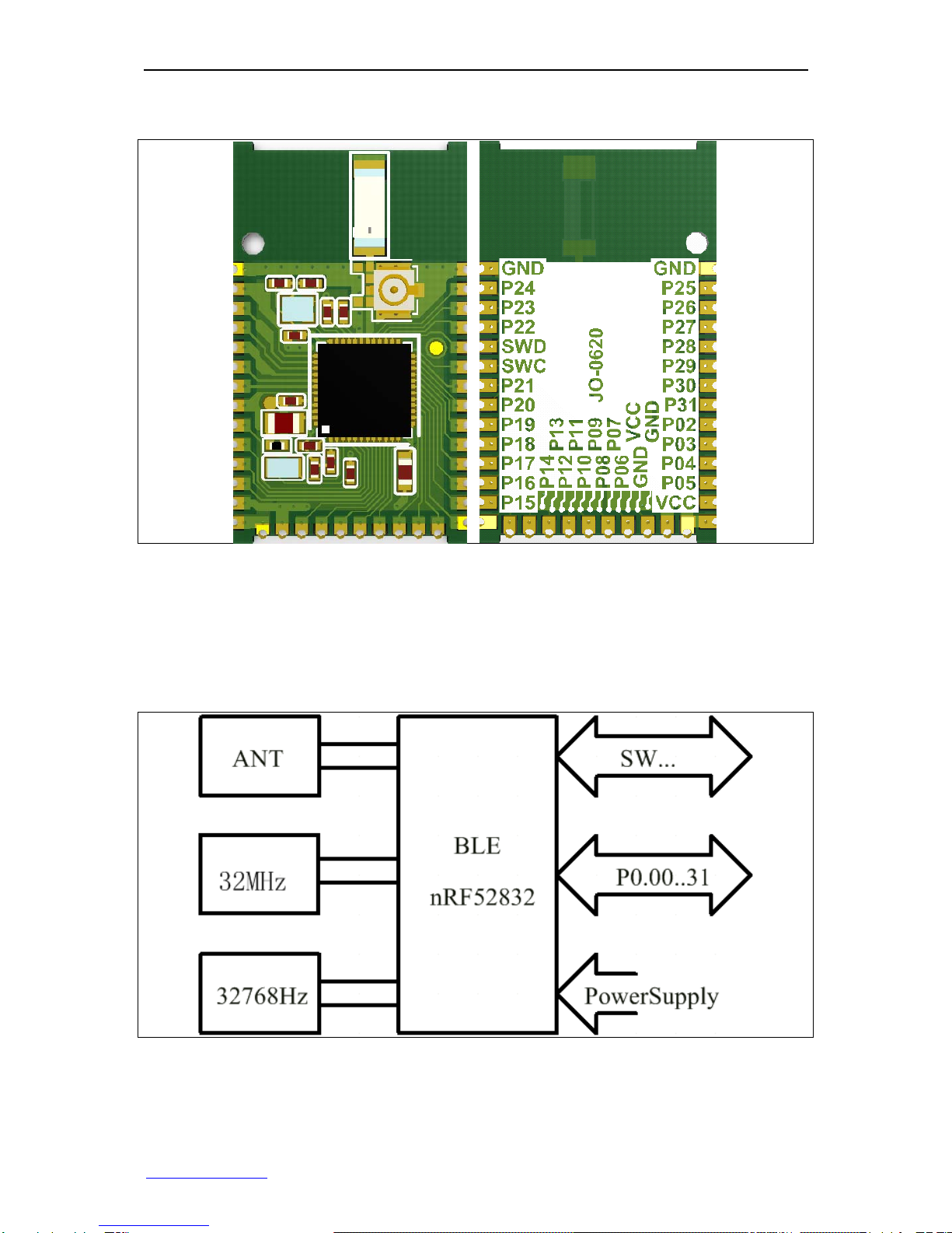
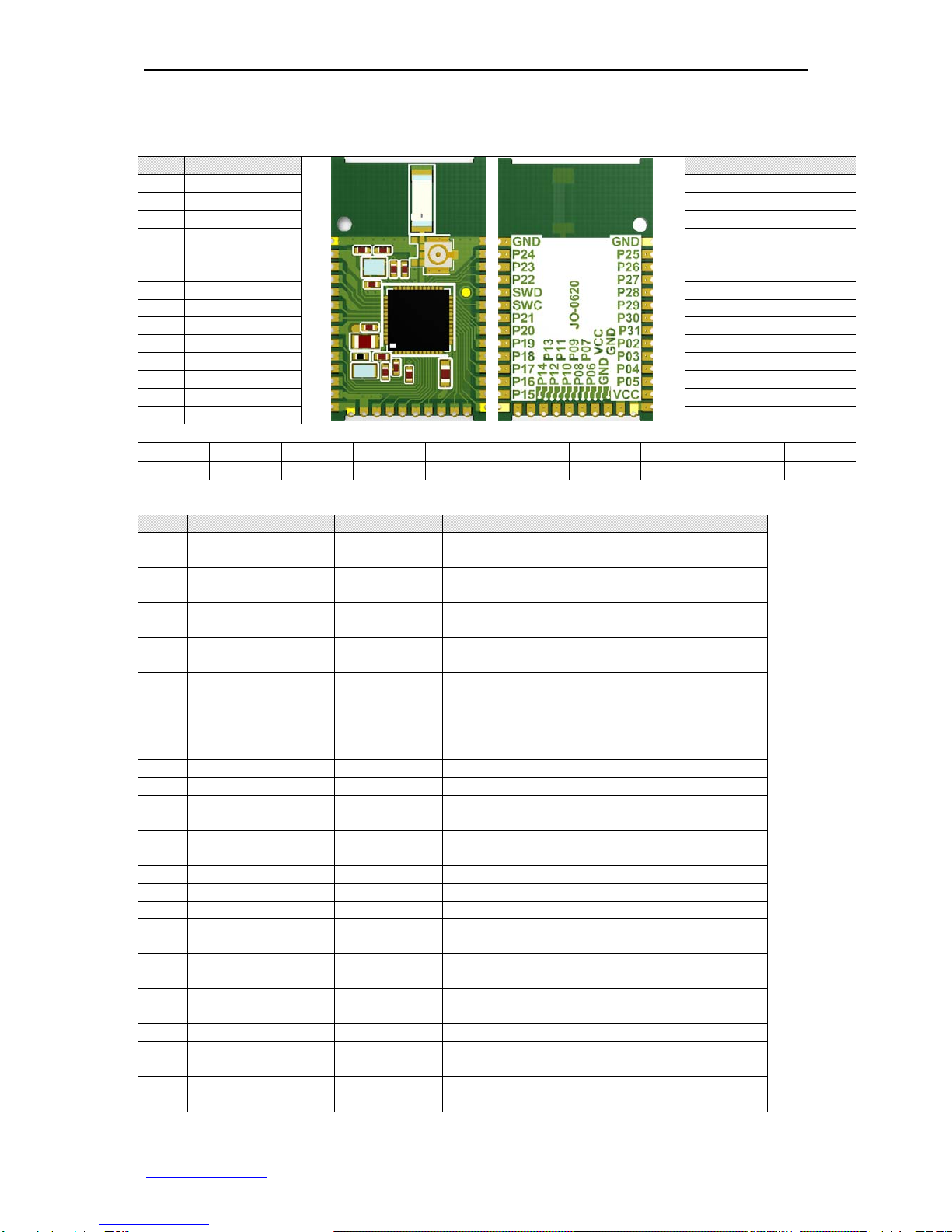
ChongQing JINOU Science & Technology BLE0305C2P Bluetooth Module Data Sheet
http://www.jinoux.com +86-23-68798999 Page 7 of 18
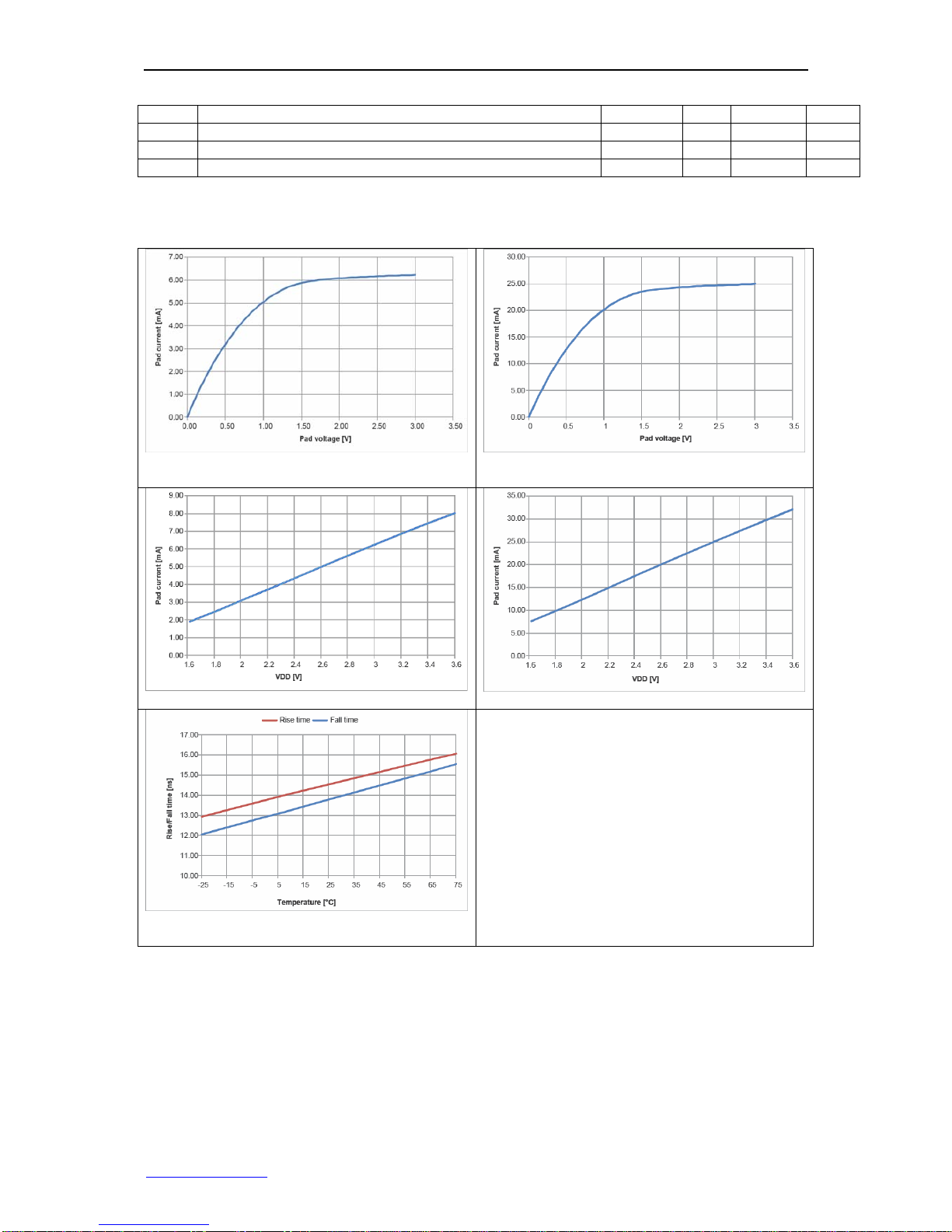
6.4. Transmitter specification
Symbol Description Min. Typ. Max. Units
PRF Maximum output power 4 6 dBm
PRFC RF power control range 24 dB
PRFCR RF power accuracy ±4 dB
PRF1,1 1st Adjacent Channel Transmit Power 1 MHz (1 Msps Nordic proprietary mode) -25 dBc
PRF2,1 2nd Adjacent Channel Transmit Power 2 MHz (1 Msps Nordic proprietary mode) -50 dBc
PRF1,2 1st Adjacent Channel Transmit Power 2 MHz (2 Msps Nordic proprietary mode) -25 dBc
PRF2,2 2nd Adjacent Channel Transmit Power 4 MHz (2 Msps Nordic proprietary mode) -50 dBc
PRF1,2,BLE 1st Adjacent Channel Transmit Power 2 MHz (2 Msps BLE mode) -20 dBc
PRF2,2,BLE 2nd Adjacent Channel Transmit Power 4 MHz (2 Msps BLE mode) -50 dBc
6.5. Receiver operation
Symbol Description Min. Typ. Max. Units
PRX,MAX Maximum received signal strength at < 0.1% BER 0 dBm
PSENS,IT,1M Sensitivity, 1Msps nRF mode 16 -93 dBm
PSENS,IT,SP,1M,BLE Sensitivity, 1Msps BLE ideal transmitter, <=37 bytes BER=1E-3 17 -96 dBm
PSENS,IT,LP,1M,BLE Sensitivity, 1Msps BLE ideal transmitter >=128 bytes BER=1E-4 18 -95 dBm
PSENS,IT,2M Sensitivity, 2Msps nRF mode 19 -89 dBm
PSENS,IT,SP,2M,BLE Sensitivity, 2Msps BLE ideal transmitter, Packet length <=37bytes -93 dBm
PSENS,DT,SP,2M,BLE Sensitivity, 2Msps BLE dirty transmitter, Packet length <=37bytes -93 dBm
PSENS,IT,LP,2M,BLE Sensitivity, 2Msps BLE ideal transmitter >= 128bytes -92 dBm
PSENS,DT,LP,2M,BLE Sensitivity, 2Msps BLE dirty transmitter, Packet length >= 128bytes -92 dBm
**16 Typical sensitivity applies when ADDR0 is used for receiver address correlation. When ADDR[1...7]
are used for receiver address correlation, the typical sensitivity for this mode is degraded by 3dB.
**17 As defined in the Bluetooth Core Specification v4.0 Volume 6: Core System Package (Low Energy
Controller Volume)
**18 Equivalent BER limit < 10E-04
**19 Typical sensitivity applies when ADDR0 is used for receiver address correlation. When ADDR[1...7]
are used for receiver address correlation, the typical sensitivity for this mode is degraded by 3dB.
6.6. selectivity
RX selectivity with equal modulation on interfering signal20
**20 Wanted signal level at PIN = -67 dBm. One interferer is used, having equal modulation
as the wanted signal. The input power of the interferer where the sensitivity equals BER
= 0.1% is presented
Symbol Description Min. Typ. Max. Units
C/I1M,co-channel 1Msps mode, Co-Channel interference 9 dB
C/I1M,-1MHz 1 Msps mode, Adjacent (-1 MHz) interference -2 dB
C/I1M,+1MHz 1 Msps mode, Adjacent (+1 MHz) interference -10 dB
C/I1M,-2MHz 1 Msps mode, Adjacent (-2 MHz) interference -19 dB
C/I1M,+2MHz 1 Msps mode, Adjacent (+2 MHz) interference -42 dB
C/I1M,-3MHz 1 Msps mode, Adjacent (-3 MHz) interference -38 dB
C/I1M,+3MHz 1 Msps mode, Adjacent (+3 MHz) interference -48 dB
C/I1M,±6MHz 1 Msps mode, Adjacent (≥6 MHz) interference -50 dB
C/I1MBLE,co-channel 1 Msps BLE mode, Co-Channel interference 6 dB
C/I1MBLE,-1MHz 1 Msps BLE mode, Adjacent (-1 MHz) interference -2 dB
C/I1MBLE,+1MHz 1 Msps BLE mode, Adjacent (+1 MHz) interference -9 dB
C/I1MBLE,-2MHz 1 Msps BLE mode, Adjacent (-2 MHz) interference -22 dB
C/I1MBLE,+2MHz 1 Msps BLE mode, Adjacent (+2 MHz) interference -46 dB
C/I1MBLE,>3MHz 1 Msps BLE mode, Adjacent (≥3 MHz) interference -50 dB
C/I1MBLE,image Image frequency Interference -22 dB
C/I1MBLE,image,1MHz Adjacent (1 MHz) interference to in-band image frequency -35 dB
C/I2M,co-channel 2Msps mode, Co-Channel interference 10 dB