XM-P55
XM-PJ1
2-6
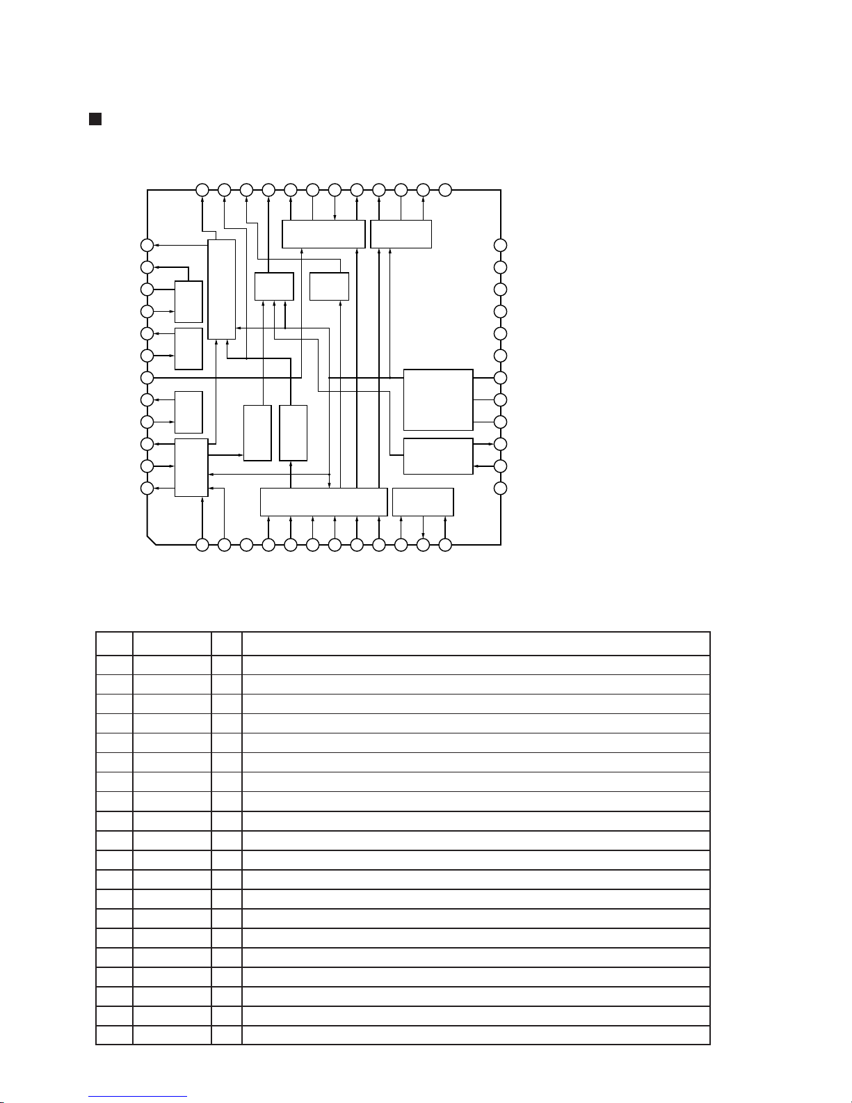
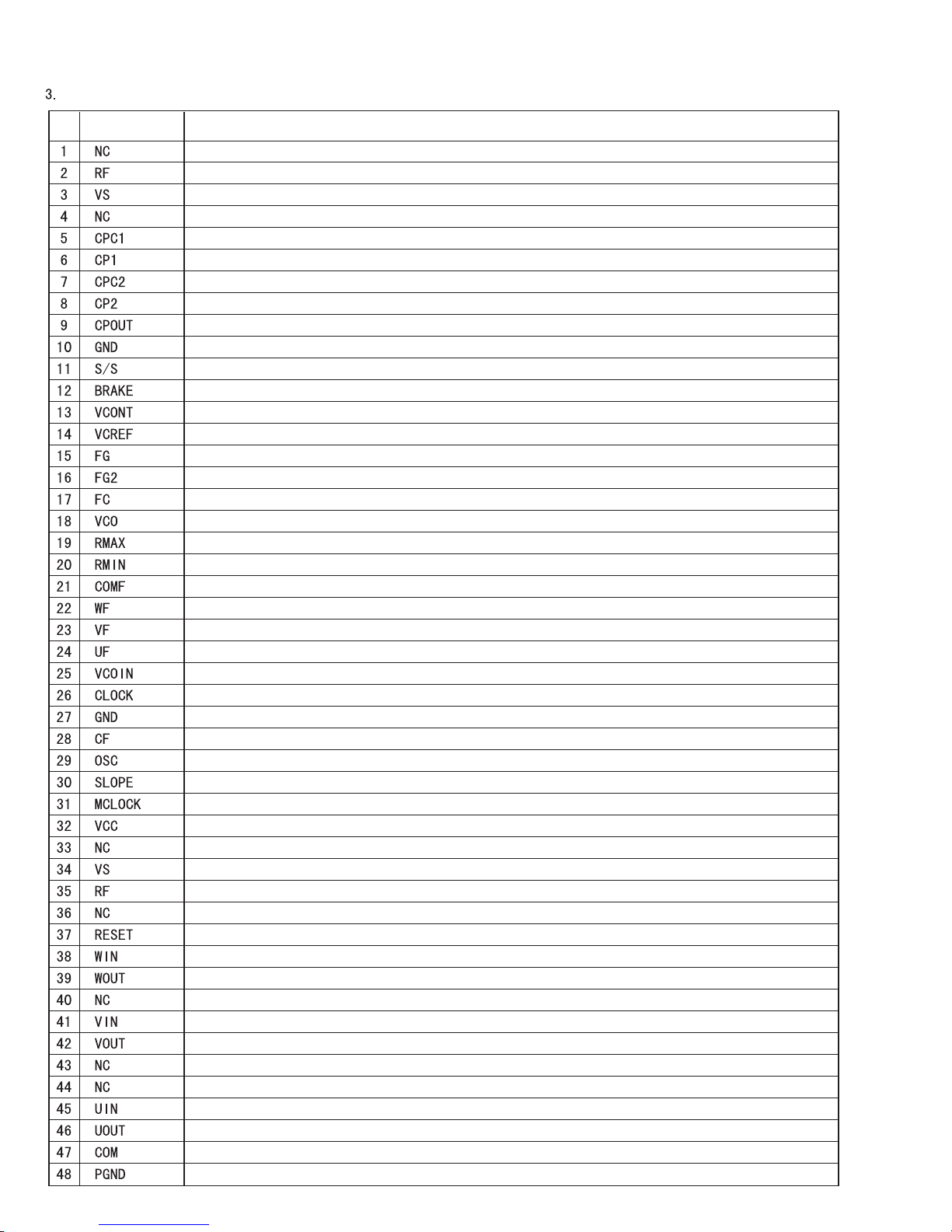
Pin Function Description
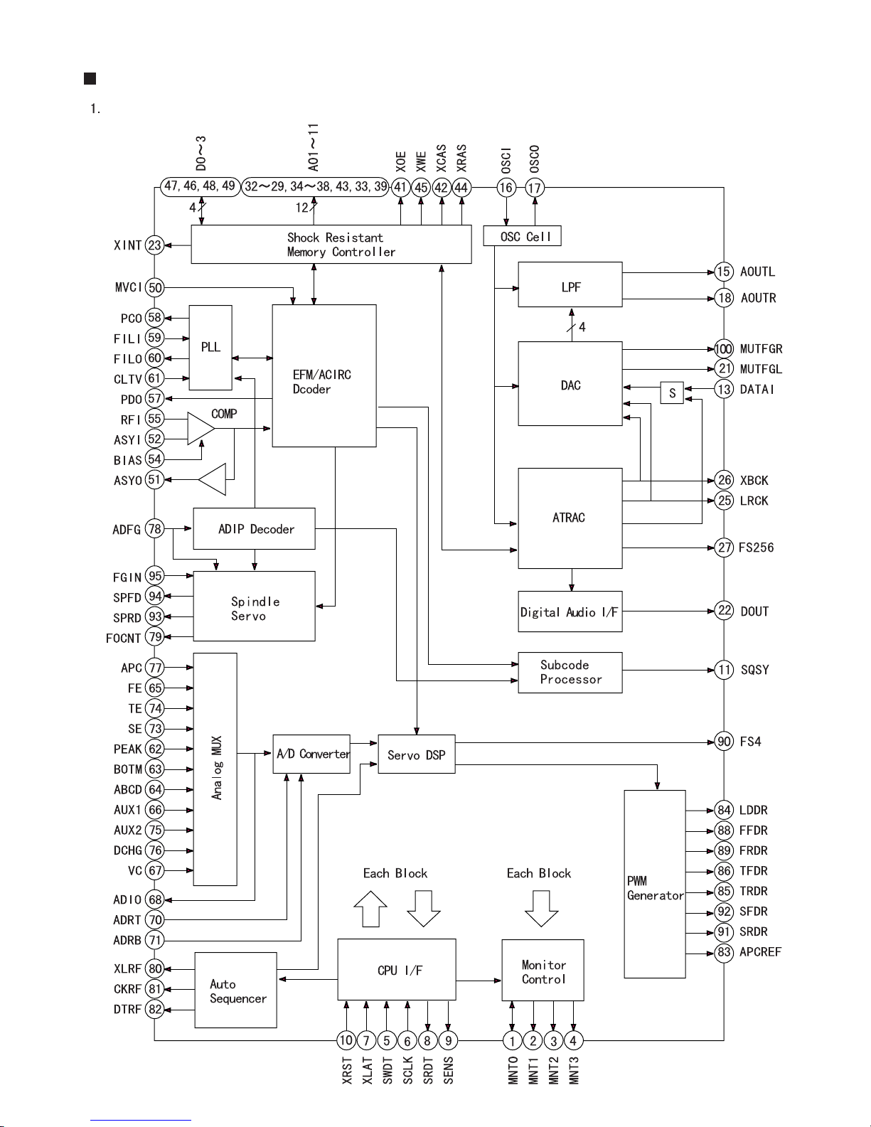
Monitor input and output
Monitor output
Monitor output
Monitor output
Data input of microcomputer serial interface
Shift lock input of microcomputer serial interface
Date output of microcomputer serial interface
Reset input L : reset
Disc sub cord Q sync / ADIP sync output
Test pin
Input of external audio data to internal DAC
DAC power supply
Integrated DAC Lch output
Crystal oscillation circuit input (512Fs=22.5792MHz)
Crystal oscillation circuit output (Inverted output of OSCI)
Integrated DAC Rch output
DAC ground
Test pin
Detection of Lch zero data / flag output
Out put of digital audio interface signal
Output of audio date to external audio block
LRCK to external audio block (44.1kHz)
Output pin (2.8224MHz)
256Fs output (11.2896MHz)
Digital power supply
External DRAM address output
External DRAM address output
External DRAM address output
External DRAM address output
External DRAM address output
External DRAM address output
External DRAM address output
External DRAM address output
External DRAM address output
External DRAM address output
External DRAM address output
Digital ground
External DRAM output enable
External DRAM CAS output
External DRAM address output
External DRAM RAS output
External DRAM write enable
External DRAM date bus
External DRAM date bus
External DRAM date bus
External DRAM date bus
External VCO (784Fs) clock input
Playback EFM full-swing output
Playback EFM comparator slice voltage input
Analog power supply
Playback EFM comparator bias current input
Playback EFM RF signal input
Analog ground
Filter input for master PLL of playback digital PLL
Filter output for master PLL of playback digital PLL
Peak hold signal input for quantity of light
Bottom hold signal input for quantity of light
Signal input for quantity of light
Focus error signal input
Auxiliary input 1
Center voltage input
Monitor output of A/D converter input signal
Analog power supply
Analog ground
Sled error signal input
Tracking error signal input
Auxiliary input 2
Connect to the low-impeddance power supply
Error signal input for laser digital APC
ADIP binary FM signal (22.05 1kHz) input
Output for setting of CXA 2523 current source
Latch output for CXA 2523 control
Shift lock output for CXA 2523 control
Data output for CXA 2523 control
Reference PWM output for laser APC
PWM output for laser digital APC
Tracking servo drive PWM output ( )
Tracking servo drive PWM output ( )
Digital power supply
Focus servo drive PWM output ( )
Focus servo drive PWM output ( )
4Fs output (176.4kHz)
Sled servo drive PWM output ( )
Sled servo drive PWM output ( )
Spindle servo drive PWM output ( )
Spindle servo drive PWM output ( )
FG input of spindle CAV servo
Test pin
Test pin
Test pin
Digital ground
Detection of Rch zero date / flag output
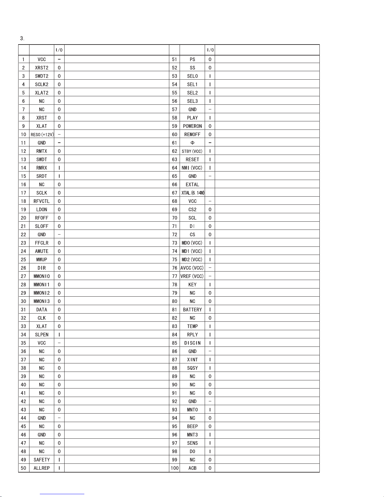
Pin
No. Symbol Functions and Operations
Latch input of microcomputer serial interface/
Latch at the Falling edge
Output of internal status corresponding to
microcomputer serial interface address
Phase comparison output for analog PLL of
EFM decoder
Phase comparison output for master PLL of
playback digital PLL
Internal VCO control voltage input for master PLL of
playback digital PLL
Input of upper-limit voltage of the A/D converter
operating range
Input of lower-limit voltage of the A/D converter
operating range
Interrupt request output L:When the interrupt
status occurs.
Pin
No. Symbol Functions and Operations