(No.52169)1-3
SECTION 1
PRECAUTION
1.1 SAFETY PRECAUTIONS
(1) The design of this product contains special hardware, many
circuits and components specially for safety purposes. For
continued protection, no changes should be made to the original
design unless authorized in writing by the manufacturer.
Replacement parts must be identical to those used in the original
circuits. Service should be performed by qualified personnel only.
(2) Alterations of the design or circuitry of the products should not be
made. Any design alterations or additions will void the
manufacturer's warranty and will further relieve the manufacturer
of responsibility for personal injury or property damage resulting
therefrom.
(3) Many electrical and mechanical parts in the products have special
safety-related characteristics. These characteristics are often not
evident from visualinspectionnor can the protectionaffordedby them
necessarily be obtained by using replacement components rated for
higher voltage, wattage, etc. Replacement parts which have these
special safety characteristics are identified in the parts list of Service
manual. Electrical components having such features are
identified by shading on the schematics and by ( ) on the
parts list in Service manual. The use of a substitute replacement
which does not have the same safety characteristics as the
recommended replacement part shown in the parts list of Service
manual may cause shock, fire, or other hazards.
(4) Use isolation transformer when hot chassis.
The chassis and any sub-chassis contained in some products are
connected to one side of the AC power line. An isolation
transformer of adequate capacity should be inserted between the
product and the AC power supply point while performing any
service on some products when the HOT chassis is exposed.
(5) Don't short between the LIVE side ground and ISOLATED (NEU-
TRAL) side ground or EARTH side ground when repairing.
Some model's power circuit is partly different in the GND. The differ-
ence of the GND is shownby the LIVE :( ) side GND, the ISOLAT-
ED (NEUTRAL) : ( ) side GND and EARTH : ( ) side GND.
Don't short between the LIVE side GND and ISOLATED (NEUTRAL)
side GND or EARTH side GND and never measure the LIVE side
GND and ISOLATED (NEUTRAL) side GND or EARTH side GND at
the same time with a measuring apparatus (oscilloscope etc.). If
above note will not be kept, a fuse or any parts will be broken.
(6) If any repair has been made to the chassis, it is recommended that
the B1 setting should be checked or adjusted (See B1 POWER
SUPPLY check).
(7) Do not check high voltage by drawing an arc. Use a high voltage
meter or a high voltage probe with a VTVM. Discharge the picture
tube before attempting meter connection, by connecting a clip lead
to the ground frame and connecting the other end of the lead
through a 10kΩ2W resistor to the anode button.
(8) When service is required, observe the original lead dress. Extra
precaution should be given to assure correct lead dress in the high
voltage circuit area. Where a short circuit has occurred, those
components that indicate evidence of overheating should be
replaced. Always use the manufacturer's replacement
components.
(9) Isolation Check (Safety for Electrical Shock Hazard)
After re-assembling the product, always perform an isolation
check on the exposed metal parts of the cabinet (antenna
terminals, video/audio input and output terminals, Control knobs,
metal cabinet, screw heads, earphone jack, control shafts, etc.) to
be sure the product is safe to operate without danger of electrical
shock.
a) Dielectric Strength Test
The isolation between the AC primary circuit and all metal parts
exposed to the user, particularly any exposed metal part having a
return path to the chassis should withstand a voltage of 1100V AC
(r.m.s.) for a period of one second.
(. . . . Withstand a voltage of 1100V AC (r.m.s.) to an appliance rat-
ed up to 120V, and 3000V AC (r.m.s.) to an appliance rated 200V
or more, for a period of one second.) This method of test requires
a test equipment not generally found in the service trade.
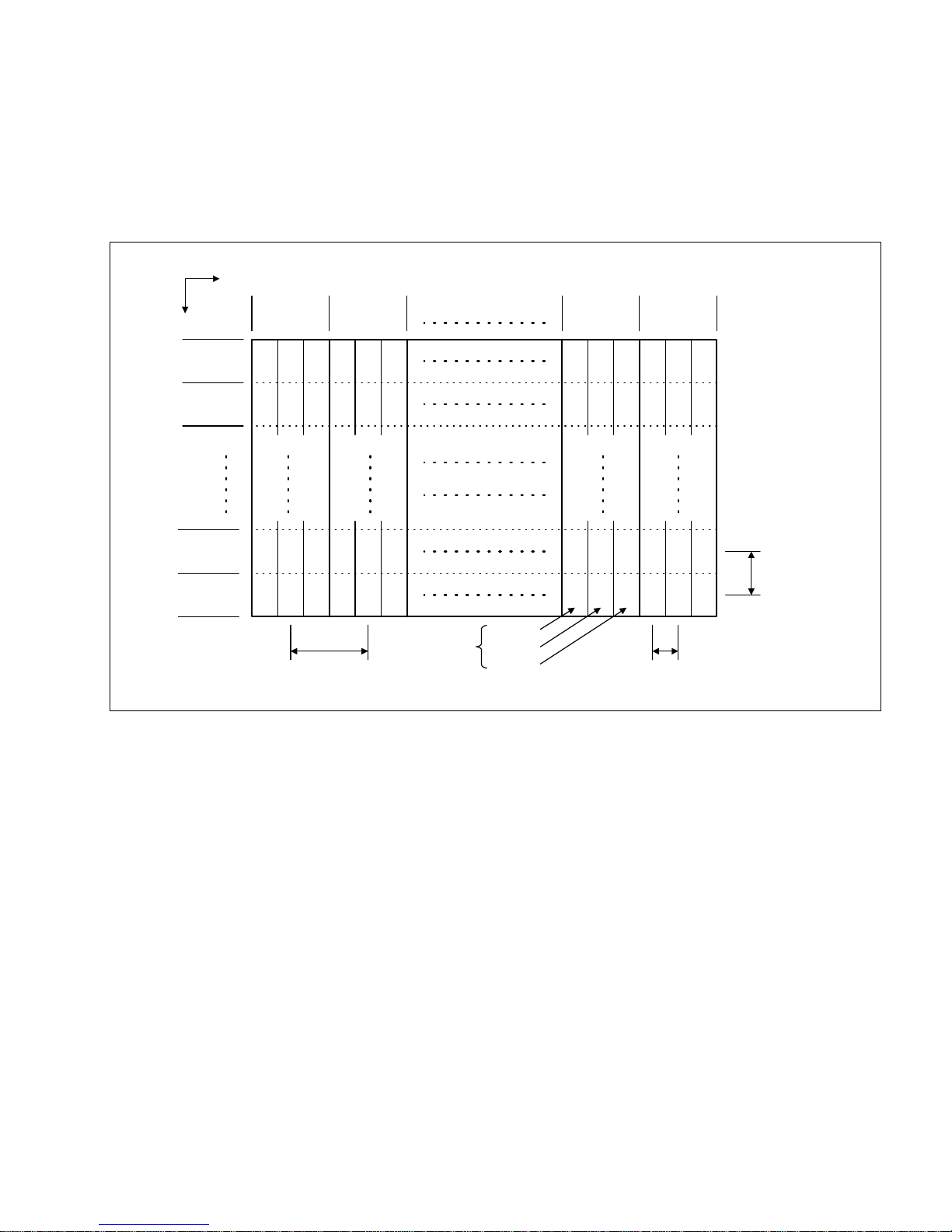
b) Leakage Current Check
Plug the AC line cord directly into the AC outlet (do not use a line
isolation transformer during this check.). Using a "Leakage
Current Tester", measure the leakage current from each exposed
metal part of the cabinet, particularly any exposed metal part
having a return path to the chassis, to a known good earth ground
(water pipe, etc.). Any leakage current must not exceed 0.5mA AC
(r.m.s.).
However, in tropical area, this must notexceed 0.2mA AC (r.m.s.).
Alternate Check Method
Plug the AC line cord directly into the AC outlet (do not use a
line isolation transformer during this check.). Use an AC
voltmeter having 1000Ωper volt or more sensitivity in the
following manner. Connect a 1500Ω10W resistor paralleled by
a0.15µF AC-type capacitor between an exposed metal part and
a known good earth ground (water pipe, etc.). Measure the AC
voltage across the resistor with the AC voltmeter. Move the
resistor connection to each exposed metal part, particularly any
exposed metal part having a return path to the chassis, and
measure the AC voltage across the resistor. Now, reverse the
plug in the AC outlet and repeat each measurement. Any
voltage measured must not exceed 0.75V AC (r.m.s.). This
corresponds to 0.5mA AC (r.m.s.).
However, in tropical area, this must not exceed 0.3V AC
(r.m.s.). This corresponds to 0.2mA AC (r.m.s.).
(10) High voltage hold down circuit check.
After repair of the high voltage hold down circuit, this circuit shall
be checked to operate correctly.See item "How to check the high
voltage hold down circuit".
AC VOLTMETER
(HAVING 1000 /V,
OR MORE SENSITIVITY)
PLACE THIS PROBE
ON EACH EXPOSED
METAL PART
1500 10W
0.15 F AC-TYPE
GOOD EARTH GROUND
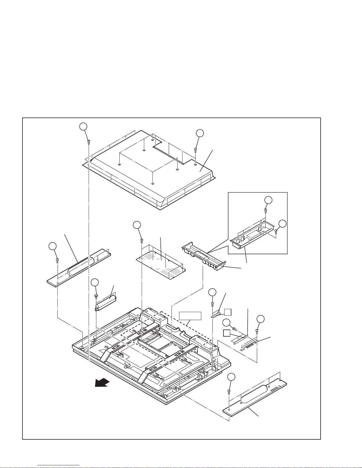
PWB
White line side
WHT
PW
POWER CORD
REPLACEMENT WARNING.
Connecting the white line side of power
cord to "WHT" character side.
A V
This mark shows a fast
operating fuse, the
letters indicated below
show the rating.