JVC I'Art Palette PD-50X795 User manual

SERVICE MANUAL
COPYRIGHT © 2005 Victor Company of Japan, Limited No.YA100
2005/2
PDP COLOR TELEVISION
YA10020052
PD-42X795/S,
PD-50X795/Z
TABLE OF CONTENTS
1 PRECAUTION. . . . . . . . . . . . . . . . . . . . . . . . . . . . . . . . . . . . . . . . . . . . . . . . . . . . . . . . . . . . . . . . . . . . . . . . . 1-3
2 SPECIFIC SERVICE INSTRUCTIONS . . . . . . . . . . . . . . . . . . . . . . . . . . . . . . . . . . . . . . . . . . . . . . . . . . . . . . 1-6
3 DISASSEMBLY . . . . . . . . . . . . . . . . . . . . . . . . . . . . . . . . . . . . . . . . . . . . . . . . . . . . . . . . . . . . . . . . . . . . . . 1-11
4 ADJUSTMENT . . . . . . . . . . . . . . . . . . . . . . . . . . . . . . . . . . . . . . . . . . . . . . . . . . . . . . . . . . . . . . . . . . . . . . . 1-28
5 TROUBLESHOOTING . . . . . . . . . . . . . . . . . . . . . . . . . . . . . . . . . . . . . . . . . . . . . . . . . . . . . . . . . . . . . . . . . 1-38
BASIC CHASSIS
FP2
TU-42X795 / TU-50X795
[RECEIVER UNIT]
VM-42X795 / VM-50X795
[PLASMA DISPLAY UNIT]
POWER
d u p
a t o
r

1-2 (No.YA100)
SPECIFICATION
Design & specifications are subject to change without notice.
Items Contents
PD-42X795 PD-50X795
Dimensions ( W ×H ×D ) Plasma Display Unit 116cm ×73.1cm ×10.8cm (45-3/4" ×28-7/8" ×4-1/4") 135cm ×83.6cm ×11cm (53-1/4" ×33" ×4-3/8")
Receiver Unit 43.5cm ×7cm ×31.3cm (17-1/4" ×2-7/8" ×12-3/8")
Mass Plasma Display Unit 38kg (83.6lbs) 51kg (112.2lbs)
Receiver Unit 4.3kg (9.5lbs)
TV RF System (Analog / Digital) Analog
Digital
CCIR (M)
ATSC terrestrial / Digital cable
Color System (Analog) NTSC
Sound System (Analog) BTSC (Multi Channel Sound)
Teletext System (Analog) Closed caption (T1-T4 / CC1-CC4)
TV Receiving Channels and
Frequency (Analog)
VHF Low
VHF High
UHF
CATV
02ch - 06ch : 54MHz - 88MHz
07ch - 13ch : 174MHz - 216MHz
14ch - 69ch : 470MHz - 806MHz
54MHz - 804MHz
Low Band : 02 - 06
High Band : 07 - 13
Mid Band : 14 - 22
Super Band : 23 - 36
Hyper Band : 37 - 64
Ultra Band : 65 - 94, 100 - 135
Sub Mid Band : 01, 96 - 99
TV / CATV Total Channel 191 Channels
Intermediate Frequency (Analog) Video IF
Sound IF
45.75 MHz
41.25 MHz (4.5MHz)
Color Sub Carrier Frequency (Analog) 3.58 MHz
Power Input AC120V, 60Hz
Power Consumption Plasma Display Unit 387.4W (Max) / 369W (Avg) 491.4W (Max) / 468W (Avg)
Receiver Unit 39.9W (Max) / 38W (Avg)
Plasma Display Panel (PDP) 42V wide aspect (16:9) 50V wide aspect (16:9)
Screen Size Diagonal : 107.5cm (H:933cm ×V : 53.3cm) Diagonal : 127.0cm (H:110.7cm ×V : 62.2cm)
Display Pixels Horizontal : 1024 pixels ×Vertical : 768 pixels (XGA) Horizontal : 1365 pixels ×Vertical : 768 pixels (W-XGA)
Audio Power Output 20W + 20W
Speaker Main (DD)
Tweeter
Woofer
9.5cm ×1cm (3-3/4 ×7-7/16"), oval type ×2
2cm (13/16"), round type ×2
13cm ×6.5cm (5-1/8 ×2-9/16"), oval type ×2
Antenna terminal (VHF/UHF, ATSC / DIGITAL CABLE IN) F-type connector, 75Ωunbalanced, coaxial ×2
Video / Audio Input
[INPUT-1/2/3/4]
Component Video
[INPUT-1/2]
1125i / 750p
525p / 525i
S-Video
[INPUT-1/3/4]
Video
Audio
RCA pin jack ×6
Y : 1V (p-p) (Sync signal: 0.35V(p-p), 3-value sync.), 75 Ω
Pb/Pr : ±0.35V(p-p), 75 Ω
Y : 1V (p-p), positive (Negative sync), 75 Ω
Pb/Pr : 0.7V(p-p), 75 Ω
Mini-DIN 4 pin ×3
Y: 1V (p-p), positive (Negative sync), 75 Ω
C: 0.286V (p-p) (Burst signal), 75 Ω
1V (p-p), positive (Negative sync), 75 Ω, RCA pin jack ×4
500mV (rms), high impedance, RCA pin jack ×8
Digital Input Video
Audio
HDMI connector ×1
(Digital-input terminal is not compatible with picture signals of computer signal)
Digital: HDMI connector ×1
Anarog: 500mV(rms) (-4dBs), high impedance, RCA pin jack ×2
Audio Output
Variable
Fix
RCA pin jack ×2
More than 0 to 1000mV (rms) (+2.2dBs)
500mV(rms), (-4dBs), low impedance (400Hz when modulated 100%)
Monitor / Recording Output S-Video
Video
Audio
Mini-DIN 4pin ×1
Y: 1V (p-p), 75Ω
C: 0.286V(p-p) (burst signal), 75Ω
1V (p-p), 75Ω, RCA pin jack ×1
250mV(rms) (-10dBs), Fs-18dB low impedance, RCA pin jack ×2
PC (RGB) Input D-sub 15pin ×1
R/G/B : 0.7V (p-p), 75Ω
HD / VD : 1V (p-p) to 5V (p-p), high impedance
< Available signal >
VGA : 640 pixels ×480 pixels (Horizontal : 31.5kHz / Vertical : 60Hz)
XGA : 1024 pixels ×768 pixels (Horizontal : 48.4kHz / Vertical : 60Hz)
Center Channel Input 500mV(rms) (-4dBs), high impedance,RCA pin jack ×1
Sub woofer Output More than 0 to 1000mV (rms) (+2.2dBs), low impedance (80Hz when modulated 100%), RCA pin jack ×1
Digital Audio Optical Output Digital SPDIF ×1
AV COMPULINK lll 3.5mm mini jack ×1
iLink Input/Output TS In/Out (4-pin, S400) ×2, IEEE1394 compliant DTCP digital copy protection compatible
Display Input / Output
(For system cable)
Control / Audio
Video
D-sub 26-pin connector ×2
DVI-D 24-pin connector ×2
Remote Control Unit RM-C14G (AA/R6 / UM-3 battery ×2)
d u p
a t o
r

(No.YA100)1-3
SECTION 1
PRECAUTION
1.1 SAFETY PRECAUTIONS
(1) The design of this product contains special hardware,
many circuits and components specially for safety
purposes. For continued protection, no changes should be
made to the original design unless authorized in writing by
the manufacturer. Replacement parts must be identical to
those used in the original circuits. Service should be
performed by qualified personnel only.
(2) Alterations of the design or circuitry of the products should
not be made. Any design alterations or additions will void
the manufacturer's warranty and will further relieve the
manufacturer of responsibility for personal injury or
property damage resulting therefrom.
(3) Many electrical and mechanical parts in the products have
special safety-related characteristics. These
characteristics are often not evident from visual inspection
nor can the protection afforded by them necessarily be
obtained by using replacement components rated for
higher voltage, wattage, etc. Replacement parts which
have these special safety characteristics are identified in
the parts list of Service manual. Electrical components
having such features are identified by shading on the
schematics and by ( ) on the parts list in Service
manual. The use of a substitute replacement which does
not have the same safety characteristics as the
recommended replacement part shown in the parts list of
Service manual may cause shock, fire, or other hazards.
(4) Don't short between the LIVE side ground and
ISOLATED (NEUTRAL) side ground or EARTH side
ground when repairing.
Some model's power circuit is partly different in the GND.
The difference of the GND is shown by the LIVE : ( ) side
GND, the ISOLATED (NEUTRAL) : ( ) side GND and
EARTH : ( ) side GND.
Don't short between the LIVE side GND and ISOLATED
(NEUTRAL) side GND or EARTH side GND and never
measure the LIVE side GND and ISOLATED (NEUTRAL)
side GND or EARTH side GND at the same time with a
measuring apparatus (oscilloscope etc.). If above note will
not be kept, a fuse or any parts will be broken.
(5) If any repair has been made to the chassis, it is
recommended that the PDP POWER SUPPLY setting
should be checked or adjusted.
(6) The high voltage applied to the PDP must conform with that
specified in Service manual. Excessive high voltage can
cause an increase in arcing and possible component
damage, therefore operation under excessive high voltage
conditions should be kept to a minimum, or should be
prevented. If severe arcing occurs, remove the AC power
immediately and determine the cause by visual inspection
(incorrect installation, cracked or melted high voltage
harness, poor soldering, etc.). To maintain the proper
components in the circuitry including the PDP must be the
exact replacements or alternatives approved by the
manufacturer of the complete product.
(7) Do not check high voltage by drawing an arc. Use a high
voltage meter or a high voltage probe with a VTVM.
Discharge the picture tube before attempting meter
connection, by connecting a clip lead to the ground frame
and connecting the other end of the lead through a 10kΩ
2W resistor to the anode button.
(8) When service is required, observe the original lead dress.
Extra precaution should be given to assure correct lead
dress in the high voltage circuit area. Where a short circuit
has occurred, those components that indicate evidence of
overheating should be replaced. Always use the
manufacturer's replacement components.
(9) Isolation Check (Safety for Electrical Shock Hazard)
After re-assembling the product, always perform an
isolation check on the exposed metal parts of the cabinet
(antenna terminals, video/audio input and output terminals,
Control knobs, metal cabinet, screw heads, earphone jack,
control shafts, etc.) to be sure the product is safe to operate
without danger of electrical shock.
a) Dielectric Strength Test
The isolation between the AC primary circuit and all metal
parts exposed to the user, particularly any exposed metal
part having a return path to the chassis should withstand a
voltage of 3000V AC (r.m.s.) for a period of one second. (.
. . . Withstand a voltage of 1100V AC (r.m.s.) to an
appliance rated up to 120V, and 3000V AC (r.m.s.) to an
appliance rated 200V or more, for a period of one second.)
This method of test requires a test equipment not generally
found in the service trade.
b) Leakage Current Check
Plug the AC line cord directly into the AC outlet (do not use
a line isolation transformer during this check.). Using a
"Leakage Current Tester", measure the leakage current
from each exposed metal part of the cabinet, particularly
any exposed metal part having a return path to the chassis,
to a known good earth ground (water pipe, etc.). Any
leakage current must not exceed 0.5mA AC (r.m.s.).
However, in tropical area, this must not exceed 0.2mA AC
(r.m.s.).
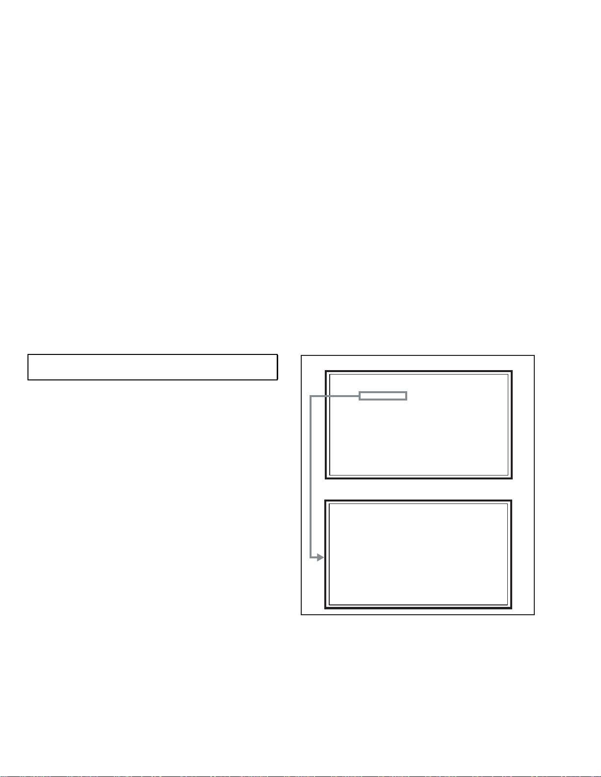
Alternate Check Method
Plug the AC line cord directly into the AC outlet (do not
use a line isolation transformer during this check.). Use
an AC voltmeter having 1000Ωper volt or more
sensitivity in the following manner. Connect a 1500Ω
10W resistor paralleled by a 0.15µF AC-type capacitor
between an exposed metal part and a known good earth
ground (water pipe, etc.). Measure the AC voltage
across the resistor with the AC voltmeter. Move the
resistor connection to each exposed metal part,
particularly any exposed metal part having a return path
to the chassis, and measure the AC voltage across the
resistor. Now, reverse the plug in the AC outlet and
repeat each measurement. Any voltage measured must
not exceed 0.75V AC (r.m.s.). This corresponds to
0.5mA AC (r.m.s.).
However, in tropical area, this must not exceed 0.3V AC
(r.m.s.). This corresponds to 0.2mA AC (r.m.s.).
AC VOLTMETER
(HAVING 1000 /V,
OR MORE SENSITIVITY)
PLACE THIS PROBE
ON EACH EXPOSED
METAL PART
1500 10W
0.15 F AC-TYPE
GOOD EARTH GROUND
d u p
a t o
r

1-4 (No.YA100)
1.2 INSTALLATION
1.2.1 HEAT DISSIPATION
If the heat dissipation vent behind this unit is blocked, cooling efficiency may deteriorate and temperature inside the unit will rise. The
temperature sensor that protects the unit will be activated when internal temperature exceeds the pre-determined level and power will
be turned off automatically.
Therefore, please make sure pay attention not to block the heat dissipation vent as well as the ventilation outlet behind the unit and
ensure that there is room for ventilation around it.
1.2.2 INSTALLATION REQUIREMENTS
Ensure that the minimal distance is maintained, as specified below, between the unit with and the surrounding walls, as well as the
floor etc. Install the unit on stable flooring or stands. Take precautionary measures to prevent the unit from tipping in order to protect
against accidents and earthquakes.
SPACE REQUIRED FOR INSTALLATION OF THE DISPLAY UNIT
SPACE REQUIRED FOR INSTALLATION OF THE RECEIVER UNIT
1.2.3 FALL TIP PREVENTION MEASURES
Take precautionary measures to prevent the unit from falling or
tipping to protect against emergencies such as earthquakes as
well as accidents.
Fasten the supplied hook for tip fall prevention using the screws,
also supplied, behind the display unit, and use them together
with durable cords (to be purchased separately) to secure the
unit to a robust part such as the wall surface or pillars.
8 inch/200 mm
2 inch/50 mm
6 inch/150 mm
6 inch/150 mm
2 inch/50 mm
4 inch/100 mm 4 inch/100 mm4 inch/100 mm 4 inch/100 mm
POWER
PLASMADISPLAY RECEIVER
The supplied hook for tipfall prevention
d u p
a t o
r

(No.YA100)1-5
1.3 PRECAUTIONS REGARDING PDP
1.3.1 PRECAUTIONS DURING NOTES FOR TRANSPORTATION
When transporting the unit, pressure exerted on the internal PDP
(Plasma Display Panel) due to improper handling (such as
tossing and dropping) may cause damages even when the unit
is carefully packed. To prevent accidents from occurring during
transportation, pay careful attention prior to delivery such as
through explaining the handling instructions to transporters.
Ensure that the following requirements are met during
transportation, as the PDP of this unit is made of glass and
therefore fragile:
(1) Avoid vibrations and impacts
The unit may be broken if it is toppled sideways even when
properly packed. Ensure that the unit is carried by at least
2 persons and pay careful attention not to exert any
vibration or impact on it.
(2) Do not place equipment horizontally
Ensure that it is placed upright and not horizontally during
transportation and storage as the PDP is very vulnerable to
lateral impacts and may break easily under such
circumstances.
During transportation, ensure that the unit is loaded along
the traveling direction of travel of the vehicle, and avoid
stacking them on one another.
For storage, ensure that they are stacked in 2 layers or less
even when placed upright.
1.3.2 RESIDUAL IMAGE / BURN-IN ON SCREEN
Like CRTs, "burn-in" may occur when a same image is
continuously displayed over an extended period of time.
As this may also shorten the life span of the PDP. Therefore, turn
off the display when not in use, scroll the screen, make use of
screen-savers, or allow even distribution on the display by
inverting the brightness, switching to complementary colors or
inserting animated images at periodic intervals.
As burn-in is more likely to occur with high brightness and
contrast settings, try to use neutral gradations or medium tone
colors.
Burn-in does not occur in the case of animated images.
When switching to another image after continuous display of the
previous image, residual images may become prominent, as
luminance in a part of the display is higher than the other parts.
This is not a defect but is because due to the discharge surface
of the lighted portion has become being relatively activated and
its luminance higher than the unlighted parts.
1.3.3 INFRARED RAYS
Near Near-infrared rays (800nm to 1000nm) are emitted from the
front of the panel, and this may give rise to malfunctions in
infrared remote controls or communication systems placed near
it. In this case, avoid direct infrared rays (and reflected rays in
some cases) from the screen by either changing the direction of
the unit or other infrared systems or securing a longer keeping a
distance from the screen.
1.3.4 OPTICAL FILTER (PANEL FILTER)
Avoid placing the unit under direct sunlight over a prolonged
period of time. This may cause the optical filter to deteriorate in
quality and color.
Clean the filter surface by wiping it softly lightly with outing
flannels a soft and lightly fuzz cloth (such as flannel).
Do not use solvents such as benzine or thinner to wipe the filter
surface. This may cause the filter to deteriorate in quality or the
coating on the surface to come off.
As the filter surface is fragile., do not scratch or hit it with hard
materials.
1.3.5 NOTES PRECAUTIONS FOR PEPLACEMENT OF
EXTERIOR PARTS
Take note of the following when replacing exterior parts (back
REAR COVER, FRONT PANEL, optical filter)
• Do not exert pressure on the front of the PDP (glass surface).
• Pay careful attention not to scratch or stain the front of the PDP
(surface) with hands.
• When replacing exterior parts, the front of the PDP should be
placed facing downward. Place a mat, etc. underneath to avoid
causing scratches to the front surface. However, never use
materials that are too soft (such as blanket cloth). If
replacement is made with the PDP surface facing downward
and in contact with the blanket, pressure may be exerted on
the PDP, thus causing damages to it.
d u p
a t o
r

1-6 (No.YA100)
SECTION 2
SPECIFIC SERVICE INSTRUCTIONS
2.1 FEATURES
D.I.S.T. (Digital Image Scaling Technology)
This system uses line interpolation to double the number of
scanning lines and achieve high resolution, flicker-free picture.
SMART CAPTION
Smart caption will appear when you press the MUTING button,
only on channels where the broadcast contains CLOSED
CAPTION information.
SMART SOUND
Decreases high sound levels, giving a regulated sound level.
VIDEO STATUS
Expression of a favorite screen can be chosen by the VIDEO
STATUS function.
[STANDARD ↔DYNAMIC ↔THEATER ↔GAME]
DIGITAL INPUT
Digital-in will display when any picture signal (480i/ 480p,
720p/ 1080i) in Digital-in is displayed.
V-CHIP
Since the V-CHIP is built in, it can choose, view and listen to a
healthy program.
MTS STEREO
The voice multiplex function of the MTS system is built in.
(MTS = Multi channel Television Sound system)
NATURAL CINEMA
Watching the movie or animation, press the Natural Cinema to
adjust the out line of the images to make thin more sharp.
BBE
High definition audio adds natural, clear and extraordinary
sound quality to any program.
VIDEO INPUT LABEL
This function is used to label video input connections for the
onscreen displays.
A.H.S.
Adds a more spacious surround sound. Music gives basic
effect and Movie for more effect.
2.2 SYSTEM SETTEING
(1) Set to 0 minutes using the [SLEEP TIMER] key.
(2) Press the [VIDEO STATUS] key and [DISPLAY] key
simultaneously, then enter the SERVICE MODE.
(3) When the Main Menu is displayed, press [2] key to enter
the self check mode.
(4) Turn off the power by pressing the [POWER] key on the
remote control unit.
Be sure to carry out the following operation at the end of
the procedure.
MAIN MENU SCREEN
SELF CHECK MODE SCREEN
LOB OK FAN OK
LOB OK FAN OK
SYNC M:OK S:OK HD:NG
TIM OK
TIM OK
MSM OK DIGI 0000
MSM OK DIGI 0000
MEM OK AVSW OK
MEM OK AVSW OK
YC OK AIO OK
YC OK AIO OK
TUN OK GCR NG 1
TUN OK GCR NG 1
IP OK RGB OK 8
IP OK RGB OK 8
DVI OK HDMI OK
DVI OK HDMI OK
SERVICE MENU
SERVICE MENU
1.ADJUST
1.ADJUST
2.SELF_CHK
2.SELF_CHK
3.I2C STOP
3.I2C STOP
d u p
a t o
r

(No.YA100)1-7
2.3 TECHNICAL INFORMATION
2.3.1 PDP STRUCTURE AND CHARACTERISTIC
This unit uses the flat type panel PDP (Plasma Display Panel), instead of the conventional CRT (Cathode Ray Tube),
as a display unit.
2.3.1.1 PIXEL (CELL) ARRAY
PDP is constructed by sealing the xenon, which emits neon and ultraviolet rays for discharging purpose, in between the electrodes
lay on the front glass substrate and rear glass substrate.
One pixel is composed of 3 RGB cells, with cell pitch of 0.280mm (1 pixel 0.810mm) [PD-50X795] / 0.304 mm (1 plxel 0.912 mm) [PD-
42X795] horizontally and 0.810mm [PD-50X795] / 0.693 mm [PD-42X795] vertically.
The cell is arrayed in each RGB color as shown in Fig. 1. One pixel is formed by interlacing each RGB color cell.
One cell size is 0.280mm [PD-50X795] / 0.304 mm [PD-42X795] horizontally and 0.810mm [PD-50X795] / 0.693 mm [PD-42X795]
vertically.
Fig.1
2.3.1.2 PIXEL DEFECTS
Though PDP is made by means of ultra precise technology, there are cases whereby not all pixels (cell) will function properly. In some
cases, there may be defective pixels that do not light at all or the ones that always light on.
There are 3 types of Pixel defects, [Bright Dot Defects], [Dark Dot Defects] and [Flicker Dot Defects], as defined respectively in the
following:
(1) BRIGHT FAULT
In this pixel fault, a cell that should not light originally is lighting on and off.
For checking this pixel fault, input ALL BLACK SCREEN and find out the cell that is lighting on and off.
(2) DARK FAULT
In this pixel fault, a cell that should light originally is not lighting or lighting with the brightness twice as brighter as originally lighting.
For checking this pixel fault, input 100% of each R/G/B colour and find out the cell that is not lighting.
(3) FLICKER FAULT
In the pixel fault, a cell that should light originally or not light originally is flashing on and off.
For checking this pixel fault, input ALL BLACK SCREEN signal or 100% of each RGB colour and find out the cell that is flashing on
and off.
B G R B G R B GRBG R
BGRBGR BGRBGR
BGRBGR BGRBGR
BGRBGR BGRBGR
No.1
Pixel
sequence
No.2
Pixel
sequence
No.1023
Pixel
sequence
No.1024
No.1365 No.1366 PD-50X795
PD-42X795
0.810mm PD-50X795
Pixel
sequence
No.1
Pixel line
No.2
Pixel line
Horizontally
Vertically
Direction
0.810mm
0.921mm 0.304mm
(Horizontally) Pixel pitch
0.280mm
(Horizontally) Cell pitch
(Vertically)
Pixel pitch(Cell pitch)
1 pixel
(1 dot)
No.767
Pixel line
No.768
Pixel line
B Cell
G
Cell
R Cell
0.693mm PD-42X795
PD-50X795
PD-42X795
PD-50X795
PD-42X795
d u p
a t o
r

1-8 (No.YA100)
2.3.2 MAIN CPU PIN FUNCTION [IC7601 = DIGITAL SIGNAL PWB ASS'Y : RECEIVER UNIT]
Pin Pin name I/O Function Pin Pin name I/O Function
1 VHOLD1 I Data slice for main screen closed caption 51 NC O Not used
2 HFLT1 I/O LPF for main screen closed caption video input 52 NC O Not used
3 NC O Not used 53 NC O Not used
4 NC O Not used 54 NC O Not used
5 DIGR0 O R [0] for OSD 55 NC O Not used
6 TB1in I AC power for timer clock 56 NC O Not used
7 REMO I Remote control 57 NC O Not used
8 BYTE I Not used 58 NC O Not used
9 CNVss I CPU programming mode select [Normal = L] 59 NC O Not used
10 DIGG0 O G [0] for OSD 60 NC O Not used
11 DIGB0 O B [0] for OSD 61 NC O Not used
12 RESET I Reset for main CPU [Reset = L] 62 HSYNC I H. sync for OSD
13 Xout O System clock osillation (crystal) : 16MHz 63 NC O Not used
14 Vss - GND 64 VSYNC I V. sync for OSD
15 Xin I System clock osillation (crystal) : 16MHz 65 NC O Not used
16 VccI I 3.3V power supply 66 NC O Not used
17 OSC1 I Clock for OSD 67 NC O Not used
18 OSC2 O Not used 68 NC O Not used
19 INT1 I AV COMPULINK control 69 NC O Not used
20 INT0 I
Request for sub(chassis) CPU communication (serial data)
70 NC O Not used
21 OUT1 O Ys (blanking) for OSD 71 NC O Not used
22 OUT2 O YM (transparence) for OSD 72 NC O Not used
23 NC O Not used 73 NC O Not used
24 NC O Not used 74 NC O Not used
25 NC O Not used 75 NC O Not used
26 NC O Not used 76 NC O Not used
27 CTA2/RTS2 O Not used 77 NC O Not used
28 CLK2 O Not used 78 NC O Not used
29 RxD2 O Data transmission (serial) for digital tuner control 79 NC O Not used
30 TxD2 I Data receive (serial) for digital tuner control 80 NC O Not used
31 SDA2 I/O Not used 81 NC O Not used
32 DIGR1 O R [1] for OSD 82 NC O Not used
33 DIGG1 O G [1] for OSD 83 NC O Not used
34 DIGB1 O B [1] for OSD 84 WAKE O
Sleep mode release for sub(chassis) CPU [Release = L]
35 TxD0 I Data receive (serial) for external programming 85 CARD_DET I Card detection for ATSC digital tuner [Detection = L]
36 RxD0 O Data transmission (serial) for external programming 86
POWER_SW
I Power switch (mechanical) detection [Detection = L]
37 CLK0 I Clock for external programming 87 SDAM I/O
Data for Inter IC (serial) bus control : main memory (IC7602)
38 RTS0 O Busy for external programming [Operation = H] 88 SCLM O
Clock for Inter IC (serial) bus control : mainmemory (IC7602)
39 P5.7 I Not used 89 DIGR2 O R [2] for OSD
40 P5.6 O Not used 90 DIGG2 O G [2] for OSD
41 HOLD I CPU programming hold [Hold = H] 91 DIGB2 O B [2] for OSD
42 P5.4 O Not used 92 NC O Not used
43 P5.3 O Not used 93 KEY2 I Key scan data for display switch button KEY2
44 P5.2 O Not used 94 KEY1 I Key scan data for display switch button KEY1
45 P5.1 O Not used 95 VHOLD2 I Data slice for sub screen closed caption
46 WR O CPU programming mode select [Normal = L] 96 HLF2 I/O LPF for sub screen closed caption video input
47 P4.7 O
Data transmission for sub(chassis) CPU communication (serial)
97 CVIN2 I Video(Y) for sub screen closed caption
48 P4.6 I
Data receive for sub(chassis) CPU communication (serial)
98 TVSETB I Test terminal [L Fixed]
49 P4.5 I Clock for sub(chassis) CPU communication (serial) 99 VCCE I 5V power supply
50 P4.4 O Not used 100 CVIN1 I Video(Y) for main screen closed caption
d u p
a t o
r

(No.YA100)1-9
2.3.3 SUB (CHASSIS) CPU PIN FUNCTION [IC7001 = DIGITAL SIGNAL PWB ASS'Y : RECEIVER UNIT]
Pin Pin name I/O Function Pin Pin name I/O Function
1 LB_PRO O Not used 51 BS_TXD O Data transmission for digital tuner communication
2 P_MU O Picture muting [Muting = H] 52 BS_RXD I Data receive for digital tuner communication
3 JP_CSB O Not used 53 NC O Not used
4 A_MU O Audio muting (for AUDIO OUT) [Muting = H] 54 VREF+ I 3.3V power supply
5 M_MU O Audio muting (for MONITOR OUT) [Muting = H] 55 PDP_TX O
Data transmission for panel CPU communication
6 PC_SEL O RGB(PC) INPUT select [ON = H] 56 PDP_RX I Data receive for
panel
CPU communication
7 ON_TIMER O POWER INDICATOR (LED) brightness [LOW = L] 57 SDA0 I/O Data for Inter IC (serial) bus : sub memory (IC7002)
8 ILA0 O Not used 58 SCL0 O Clock for Inter IC (serial) bus : sub memory (IC7002)
9 ILA1 O Not used 59 SDA_DVI I/O Data for Inter IC (serial) bus for panel communication
10 ILA2 O Not used 60 SCL_DVI O Clock for Inter IC (serial) bus for panel communication
11 POW_LED O POWER LED lighting [ON = H] 61 AVSS - GND
12 WORD O Not used 62 DIGI_PHOT I Photo sensor for DIGITAL-IN illegal copy protection
13 MI_CK I Clock for main CPU communication 63 AGC I Not used
14 MI_TX I Data receive for main CPU communication 64 EXT_YS1 I Not used
15 MI_RX O Data transmission for main CPU communication 65 EXT_YS2 I Not used
16 MI_REQ O
Data request for main CPU communication [Request = L]
66 VDD I 3.3V power supply
17 VDD I 3.3V power supply 67 DIGI_PRO O DIGITAL-IN voltage detection [Detection = H]
18 FOSC O Not used 68 GCR_RST O Not used
19 VSS - GND 69 GR_ON O Not used
20 X1 I 3.3V power supply 70 SYNC_SEL O Multi screen control [Digital = L]
21 X0 O Not used 71 NC O Not used
22 VDD I 3.3V power supply 72 NC O Not used
23 OSC1 I System clock osillation (crystal) : 16MHz 73 SBD5 I/O
Data for writing on board (connect CN01P : for Frash ROM type)
24 OSC0 O System clock osillation (crystal) : 16MHz 74 SBT5 I
Clock for writing on board (connect CN01P : for Frash ROM type)
25 MODE I 3.3V power supply 75 NMI I 3.3V power supply
26 BS1.5CTL O Digital tuner power control [ON = H] 76 COMP I Not used
27 A92RES O
Reset for IC1001(3D YC SEP / COLOR DEMODULAT) [Reset = H]
77 REMO I Remote control
28 BS_RST O Reset for Digital tuner [Reset = L] 78 VSYNC I V. sync pulse
29 LIP_RST O Not used 79 WAKE I
Sleep mode release for sub(chassis) CPU [Release = L]
30 SOFT_OFF O Not used 80
POWERGOOD
I Power error detection NG = H]
31 VMUTE I Picture muting request from digital tuner [Muting = L] 81 NC O Not used
32 VOUTENB O Video cutoff for digital tuner [Cufoff = H] 82 RST I Reset for
sub(chassis)
CPU [Reset = L]
33 MDR_CON I System cable connection monitor for display unit (PDP) 83 VDD I 3.3V power supply
34 AVDD I 3.3V power supply 84 SCL3A O Clock for Inter IC (serial) bus control
35 BS_POW O Not used 85 SDA3A I/O Data for Inter IC (serial) bus control
36
DsyncSW2
O Sync select for DIGITAL-IN [Cotrolled with 99-pin] 86 SCL3B O Clock for Inter IC (serial) bus control
37 LB_POW O Not used 87 SDA3B I/O Data for Inter IC (serial) bus control
38 NC O Not used 88
DIGI_SYNCSEL
O Not used
39 HOTPLUG I Video communiation monitor for display unit (PDP) 89 DIGI_LRSW O DIGITAL-IN control
40 MECA_SW I Mechanical monitor for POWER switch [Push = L] 90 DIGI_INT I Reset for HDMI process [Reset = L ]
41 MAIN_POW O Main power control [ON = L] 91 DVI_RST O Reset for DVI format conversion
42 MSP_RST O AUDIO OUT output mode select [VARIABLE = L] 92 VSS - GND
43 VREF- I Standard Voltage (0V) power supply 93 SCL5055 O
Clock for Inter IC (serial) bus : JCC5055 (DIST process)
44 AFT2 I Not used 94
VFORMATSEL
O Not used
45 AFT1 I AFT voltage for VHF/UHF tuner 95 SDA5055 I/O Data for Inter IC (serial) bus : JCC5055 (DIST process)
46 KEY2 I Not used 96
OSD_MODE_SEL
O Not used
47 KEY1 I Not used 97 NC O Not used
48 NC O Not used 98 15K/OTH O Main video select [Fixed H]
49 NC O Not used 99 DsyncSW1 O Sync select for DIGITAL-IN [Cotrolled with 36-pin]
50 AC_IN I AC power pulse for timer clock 100 57 BUSY I Busy monitor for JCC5057 (RGB process)
d u p
a t o
r

1-10 (No.YA100)
2.3.4 PANEL CPU PIN FUNCTION [IC807 = DISPLAY INTERFACE PWB ASS'Y : DISPLAY UNIT]
Pin Pin name I/O Function Pin Pin name I/O Function
1 SYSTEM0 I PDP size select [0V=50V XGA, 1.75V=42V XGA] 34 NC O Not used
2 SYSTEM3 I PDP maker select [0V=SAMSUNG, 1.75V=LG] 35 NMI I Port for writing on board control [Writing=L]
3 AVCC - 5.0V power suplly 36 A_MU O Audio muting [Muting=H]
4 X2 - Not used 37 HD I Not used
5X1 -GND 38
LED_ONTIMER
O POWER LED stand-by control [ON=H]
6 VCL - GND 39 REMO I Not used
7 RES I Reset for panel CPU [Reset=L] 40 LED_POW O POWER LED control [ON=H]
8 TEST I GND 41 P85 I
Emulator connection / Port for writing on board [Writing=H]
9 VSS - GND 42 P86 - Emulator connection
10 OSC2 O System clock osillation (crystal) : 16MHz 43 P87 - Emulator connection
11 OSC1 I System clock osillation (crystal) : 16MHz 44 SCK3 O Clock for writing on board
12 VCC - 5.0V power suplly 45 RXD I Data receive for writing on board
13 PW_LOB O Power control [ON=L] 46 TXD O Data trnsmission for writing on board
14
PANEL_PW_ON
O Panel power control [ON=L] 47 AC_DET I AC power frequency detection [Detection=H]
15 NC O Not used 48 NC O Not used
16 NC O Not used 49 RXD2 I Data receive for main CPU communication
17 I2C_STOP O Inter IC (serial) bus stop control [Stop=L] 50 TXD2 O Data transmission for main CPU communication
18 APL_S_CLK O Clock for APS loading [PD-50X795] 51 IRQ O Sleep mode release [Rlease=H]
19 PSCK O Clock for APS writing [PD-50X795] 52 ACTIVE I Power switch (mechanical) detection [Detection=H]
20 PLE O APS loading control [PD-50X795] 53 VD I V. sync pulse
21 CLE O APS writing control [PD-50X795] 54 REC_DET I System cable monitor for receiver unit [Connection=L]
22 PSSC O Data transmission for APS loading [PD-50X795] 55 PSS I PDP Inter IC (serial) bus communication select
[Permission=H][PD-42X795],
Data receive for APS loading [PD-50X795]
23 SDA1 I/O
Data for Inter IC (serial) bus control : panel memory (IC805)
24 PWM O Not used
25 SCL1 O
Clock for Inter IC (serial) bus control : panel memory (IC805)
56 FAN_LOCK I Fan abnormality detection [Detection=L] [PD-50X795]
26 SDA0 I/O
Data for Inter IC (serial) bus control : Audio control, Temp. sensor
57 SYSTEM2 I Not used
27 SCL0 O
Clock for Inter IC (serial) bus control : Audio control, Temp. sensor
58 SYSTEM 1 I Fan select [Used=H]
28 SDA2 I/O
Data for Inter IC (serial) bus control : PDP communication
59 THEM_DET I Temp. sensor detection [Detection=H]
29 SCL2 O
Clock for Inter IC (serial) bus control : PDP communication
60
(AMP_PRO2)
IGND
30 SLE O PDP communication control [PD-50X795] 61 AMP_PRO1 I Not used
31 NC I/O Not used 62 EE_CDS I Not used
32 NC O Not used 63 KEY1 I Not used
33 NC O Not used 64 KEY2 I Not used
d u p
a t o
r

(No.YA100)1-11
SECTION 3
DISASSEMBLY
3.1 DISASSEMBLY PROCEDURE [DISPLAY UNIT: PD-42X795]
NOTE:
• When exchanging parts etc. with the front side (PDP side) fancing down, place a protection sheet under the DISPALY UNIT to
prevent scratches on the front side.
• It is advisable to take notes of the connecting locations (connector numbers) of the removed connectors.
3.1.1 REMOVING THE REAR COVER (Fig.1)
(1) Remove the power cord and system cable.
(2) Remove the 9 screws [A] and the 12 screws [B], then
remove the REAR COVER.
3.1.2 REMOVING THE BACK COVER AND SPEAKER
HOLDER (Fig.1)
(1) Remove the 8 screws [C], then remove the BACK COVER.
(2) Remove the SPEAKER HOLDER.
3.1.3 REMOVING THE TERMINAL COVER (Fig.1.)
• Remove the REAR COVER.
(1) Remove the 6 screws [D], then remove the CHASSIS
SHIELD BRACKET.
(2) Remove the 2 screws [E] and the 5 screws [F], then
remove the TERMINAL COVER.
3.1.4 REMOVING THE LINE FILTER PWB (Fig.1)
• Remove the REAR COVER.
• Remove the CHASSIS SHIELD BRACKET.
• Remove the TERMINAL COVER.
(1) Remove the 2 claws [G], then remove the LINE FILTER
INSULATOR.
(2) Disconnect the connector [CN8001] from the MAIN
POWER PWB .
(3) Remove the 2 screws [H] and the 2 screws [I], then remove
the LINE FILTER PWB.
3.1.5 REMOVING THE AUDIO PWB (Fig.1)
• Remove the REAR COVER.
• Remove the CHASSIS SHIELD BRACKET.
• Remove the TERMINAL COVER.
(1) Disconnect the connectors [CN60SL] / [CN60CB] /
[CN60SR] from the AUDIO PWB .
(2) Disconnect the connector [CN9001] from the SUB POWER
PWB.
(3) Disconnect the connector [CN00A] / [CN00C] / [CN00D]
from the DISPLAY INTERFACE PWB .
(4) Remove the 4 screws [J], then remove the AUDIO PWB.
3.1.6 REMOVING THE DISPLAY INTERFACE PWB (Fig.1)
• Remove the REAR COVER.
• Remove the CHASSIS SHIELD BRACKET.
• Remove the TERMINAL COVER.
(1) Disconnect the connectors [CN00A] / [CN00C] / [CN00D] /
[CN00E] / [CN00Q] / [CN00T] / [CN00X] / [CN00V] /
[CNAH2] from the DISPLAY INTERFACE PWB .
(2) Remove the 4 screws [K], the 2 screws [L] ,and the 2
screws [M], then remove the DISPLAY INTERFACE PWB.
3.1.7 REMOVING THE CHASSIS BASE PWB (Fig.1.)
• Remove the REAR COVER.
• Remove the CHASSIS SHIELD BRACKET.
• Remove the TERMINAL COVER.
• Remove the LINE FILTER PWB.
• Remove the AUDIO PWB.
• Remove the DISPLAY INTERFACE PWB.
(1) Remove the 2 screws [N], then remove the CHASSIS
BASE PWB.
d u p
a t o
r

1-12 (No.YA100)
Fig.1
a
a
TOP
A
C
B
A
C
CHASSIS BASE
CHASSIS SHIELD
BRACKET E
H
F
F
E
F
F
BACK COVER
BACK COVER
REAR COVER
J
K
D
AUDIO
PWB
DISPLAY
INTERFACE
PWB
LINE
FILTER
PWB
INSULATOR
I
I
N
N
M
L
G
TERMINAL
COVER
SPEAKER HOLDER
SPEAKER HOLDER
d u p
a t o
r

(No.YA100)1-13
3.1.8 REMOVING THE TEMP. SENSOR PWB (Fig.2)
• Remove the REAR COVER.
(1) Disconnect the connector [CN800V] from the TEMP.
SENSOR PWB PWB .
(2) Remove the 1 screw [O], then remove the TEMP.
SENSOR PWB.
3.1.9 REMOVING THE MAIN POWER PWB (Fig.2)
• Remove the REAR COVER.
(1) Disconnect the connector [CN8001] / [CN8008] / [CN8006]
/ [CN8005] / [CN8003] / [CN8002] / [CN9001] / [CN8009]
from the MAIN POWER PWB .
(2) Remove the 8 screws [P], then remove the MAIN POWER
PWB.
(3) Remove the POWER PWB BRACKET and INSULATOR.
3.1.10 REMOVING THE SUB POWER PWB (Fig.2)
• Remove the REAR COVER.
(1) Disconnect the connector [CN9001] / [CN9002] / [CN9005]
from the SUB POWER PWB .
(2) Remove the 4 screws [Q], then remove the SUB POWER
PWB.
(3) Remove the INSULATOR.
3.1.11 REMOVING THE DISPLAY SWITCH PWB (Fig.2)
• Remove the BACK COVER.
• Remove the SPEAKER HOLDER.
(1) Remove the 2 screws [U] and 3 screws [V], then remove
the DISPLAY SWITCH PWB and CONTROL KNOB.
(2) Disconnect the connector [CN000T] from the DISPLAY
SWITCH PWB .
3.1.12 REMOVING THE DISPLAY LED PWB (Fig.2)
• Remove the BACK COVER.
• Remove the SPEAKER HOLDER.
• Remove the DISPLAY SWITCH PWB.
(1) Remove the 2 screws [T], then remove the DISPLAY LED
PWB.
(2) Disconnect the connector [CN000X] from the DISPLAY
LED PWB .
3.1.13 REMOVING THE DD SPEAKER (Fig.2)
• Remove the REAR COVER.
• Remove the BACK COVER.
• Remove the SPEAKER HOLDER.
(1) Disconnect the connector [CN60SR] / [CN60SL] from the
AUDIO PWB .
(2) Remove the 4 screws [U], then remove the DD SPEAKER.
3.1.14 REMOVING THE WOOFER SPEAKER (Fig.2)
• Remove the REAR COVER.
(1) Disconnect the connector [CN60CB] from the AUDIO
PWB.
(2) Remove the 6 screws [V], then remove the WOOFER
SPEAKER UNIT.
(3) Remove the 8 screws [W], then remove the DUCT
COVER.
(4) Remove the 12 screws [X], then remove the WOOFER
BACK COVER.
(5) Remove the 8 screws [Y], then remove the WOOFER
SPEAKER.
3.1.15 REMOVING THE PDP (PANEL) UNIT (Fig.2)
• Remove the REAR COVER.
• Remove the CHASSIS SHIELD BRACKET.
• Remove the TERMINAL COVER.
• Remove the CHASSIS BASE(with each PWB affixed on the
CHASSIS BASE).
• Remove the TEMP. SENSOR.
• Remove the MAIN POWER PWB.
• Remove the SUB POWER PWB.
(1) Disconnect the connector [CN60SL] / [CN60CB] /
[CN60SR] from the AUDIO PWB .
(2) Disconnect the connector [CN00A] / [CN00C] / [CN00D] /
[CN00E] / [CN00Q] / [CN00T] / [CN00X] / [CN0V] /
[CNAH2] from the DISPLAY INTERFACE PWB.
(3) Remove the 16 screws [Z], then remove the BACK
BRACKET.
(4) Lift the PDP upright and remove it with enough care not to
impose shock to the PDP.
CAUTION:
• Two or more people are required to remove the PDP unit.
• The gas pouring port is covered with the protection
material.In operation, be careful not to damage the gas
pouring port.
• Do not touch the front side (glass) of the PDP with your
fingers.
d u p
a t o
r

1-14 (No.YA100)
Fig.2
TOP
GAS insertion
hole
X
W
W
Y
X
V
BACK FRAME
BRACKET
MAIN POWER PWB
POWER PWB
BRACKET
INSULATOR
SUB POWER PWB
BACK FRAME
BRACKET INSULATOR
INSULATOR
TEMP.
SENSOR PWB
PDP UNIT
Z
Y
RS
T
DD SPEAKER
DD SPEAKER
DISPLAY
SWITCH
PWB
INSULATOR
DISPLAY LED PWB
DUCT
COVER
DUCT COVER WOOFER BACK
COVER
WOOFER
SPEAKER
WOOFER
SPEAKER
CONTROL
KNOB
O
U
U
P
Q
Q
Z
P
Z
P
Z
d u p
a t o
r

(No.YA100)1-15
3.1.16 REMOVING THE PWB IN PDP UNIT
3.1.16.1 REMOVING THE LOGIC-BUFFER-E PWB (Fig.3)
• Remove the PDP UNIT.
(1) Disconnect the connector [CN806] / [CN2500] / [CN2501] /
[CN2502] / [CN2503] / [CN2504] / [CN2505] / [CN2506] /
[CN2507] / [EF1] from the LOGIC-BUFFER-E PWB .
(2) Remove the 14 screws [a], then remove the LOGIC-BUFF-
ER-E PWB.
3.1.16.2 REMOVING THE LOGIC-BUFFER-F PWB (Fig.3)
• Remove the PDP UNIT.
(1) Disconnect the connector [CN402] / [CN807] / [CN2600] /
[CN2601] / [CN2602] / [CN2603] / [CN2604] / [CN2605] /
[CN2606] / [CN2607] / [FE1] from the LOGIC-BUFFER-F
PWB .
(2) Remove the 14 screws [b], then remove the LOGIC-BUFF-
ER-F PWB.
3.1.16.3 REMOVING THE X-MAIN PWB (Fig.3.)
• Remove the PDP UNIT.
(1) Disconnect the connector [CN4001] / [CN4002] / [CN4003]
/ [CN4004] / [CN4005] from the X-MAIN PWB .
(2) Remove the 8 screws [c], then remove the X-MAIN PWB.
3.1.16.4 REMOVING THE LOGIC-MAIN PWB (Fig.3)
• Remove the PDP UNIT.
(1) Disconnect the connector [CN2001] / [CN2002] / [CN2003]
/ [CN2004] / [CN2005] / [CN2006] / [CN207] / [LA1] from
the LOGIC-MAIN PWB .
(2)
Remove the 6 screws
[d]
, then remove the LOGIC-MAIN PWB.
3.1.16.5 REMOVING THE Y-MAIN PWB (Fig.3.)
• Remove the PDP UNIT.
(1) Disconnect the connector [CN5001] / [CN5002] / [CN5003]
/ [CN5004] / [CN5005] / [CN5006] / [CN5007] / [CN5008]
from the Y-MAIN PWB .
(2) Remove the 7 screws [e], then remove the Y-MAIN PWB.
3.1.16.6 REMOVING THE Y-BUFFER-U PWB (Fig.3)
• Remove the PDP UNIT.
(1)
Disconnect the connector [CN5401] / [CN5402] / [CN5403] /
[CN5404] / [CN5405] / [CN5407] from the Y-BUFFER-U PWB.
(2)
Remove the 3 screws
[f]
,then remove the Y-BUFFER-U PWB
.
3.1.16.7 REMOVING THE Y-BUFFER-L PWB (Fig.3)
• Remove the PDP UNIT.
(1)
Disconnect the connector [CN5501] / [CN5502] / [CN5503] /
[CN5504] / [CN5505] / [CN5507] from the Y-BUFFER-L PWB.
(2)
Remove the 3 screws
[g]
, then remove the Y-BUFFER-L PWB
.
Fig.3
c
a
b
f
g
e
b
a
X-MAIN PWB
LOGIC-BUFFER-E PWB
LOGIC-BUFFER-F PWB
Y
-BUFFER-U PWB
Y-MAIN PWB
Y-BUFFER-L PWB
LOGIC-BUFFER-E PWB
LOGIC-MAIN PWB
LOGIC-BUFFER-F PWB
d
d u p
a t o
r

1-16 (No.YA100)
3.1.17 REMOVING THE FRONT FILTER (Fig.4.)
• Remove the REAR COVER.
• Remove the CHASSIS SHIELD BRACKET.
• Remove the TERMINAL COVER.
• Remove the CHASSIS BASE (with each PWB affixed on the
CHASSIS BASE).
• Remove the TEMP. SENSOR.
• Remove the MAIN POWER PWB.
• Remove the SUB POWER PWB.
• Remove the PDP UNIT.
(1) Remove the 12 screws [h], then remove the GLASS
HOLDER.
(2) Remove the FRONT FILTER with enough care not to
damage it.
3.1.18 REMOVING THE TOP FRAME BRACKET, BOTTOM
FRAME BRACKET AND SIDE FRAME BRACKET (Fig.
4
.)
• Remove the REAR COVER.
• Remove the CHASSIS SHIELD BRACKET.
• Remove the TERMINAL COVER.
• Remove the CHASSIS BASE (with each PWB affixed on the
CHASSIS BASE).
• Remove the TEMP. SENSOR.
• Remove the MAIN POWER PWB.
• Remove the SUB POWER PWB.
• Remove the PDP UNIT.
• Remove the FRONT FILTER.
(1)
Remove the 6 screws
[i]
,
then remove
the FRONT PANEL
.
(2) Remove the 4 spacers [j], the 4 screws [k], then remove
the TOP FLAME BRACKET, BOTTOM FLAME BRACKET
and SIDE FLAME BRACKET.
Fig.4
TOP
GLASS HOLDER
SIDE FRAME
BRACKET
SIDE FRAME
BRACKET
TOP FRAME
BRACKET
BOTTOM FRAME
BRACKET
FRONT FILTER
FRONT PANEL
j
i
i
i
i
k
k
h
h
j
j
j
d u p
a t o
r

(No.YA100)1-17
3.2 DISASSEMBLY PROCEDURE [DISPLAY UNIT: PD-50X795]
NOTE:
• When exchanging parts etc. with the front side (PDP side) fancing down, place a protection sheet under the DISPALY UNIT to
prevent scratches on the front side.
• It is advisable to take notes of the connecting locations (connector numbers) of the removed connectors.
3.2.1 REMOVING THE REAR COVER (Fig.5)
(1) Remove the power cord and the system cable.
(2) Remove the 11 screws [A] and the 22 screws [B], then
remove the REAR COVER.
3.2.2 REMOVING THE BACK COVER AND SPEAKER
HOLDER (Fig.5)
(1) Remove the 8 screws [C], then remove the BACK COVER.
(2) Remove the SPEAKER HOLDER.
3.2.3 REMOVING THE TERMINAL COVER (Fig.5)
• Remove the REAR COVER.
(1) Remove the 6 screws [D], then remove the CHASSIS
SHIELD BRACKET.
(2) Remove the 2 screws [E] and the 5 screws [F], then
remove the TERMINAL COVER.
3.2.4 REMOVING THE LINE FILTER PWB (Fig.5)
• Remove the REAR COVER.
• Remove the CHASSIS SHIELD BRACKET.
• Remove the TERMINAL COVER.
(1) Remove the 2 claws [G], then remove the LINE FILTER
INSULATOR.
(2) Disconnect the connector [CN8001] from the MAIN
POWER UNIT.
(3) Remove the 2 screws [H] and 2 screws [I], then remove the
LINE FILTER PWB.
3.2.5 REMOVING THE AUDIO PWB (Fig.5.)
• Remove the REAR COVER.
• Remove the CHASSIS SHIELD BRACKET.
• Remove the TERMINAL COVER.
(1) Disconnect the connector [CN60SL] / [CN60CB] /
[CN60SR] from the AUDIO PWB .
(2) Disconnect the connector [CN9001] from the SUB POWER
PWB.
(3) Disconnect the connector [CN00A] / [CN00C] / [CN00D]
from the DISPLAY INTERFACE PWB.
(4) Remove the 4 screws [J], then remove the AUDIO PWB.
3.2.6 REMOVING THE DISPLAY INTERFACE PWB (Fig.5)
• Remove the REAR COVER.
• Remove the CHASSIS SHIELD BRACKET.
• Remove the TERMINAL COVER.
(1) Disconnect the connector [CN00A] / [CN00C] / [CN00D] /
[CN00E] / [CN00G] / [CN00Q] / [CN00T] / [CN00X] /
[CN00V] / [CN0FL] / [CN0FR] / [CN601] / [CNAH1] from the
DISPLAY INTERFACE PWB .
(2) Remove the 3 screws [K], the 2 screws [L] and 2 screws
[M] , then remove the DISPLAY INTERFACE PWB.
3.2.7 REMOVING THE CHASSIS BASE (Fig.5)
• Remove the REAR COVER.
• Remove the CHASSIS SHIELD BRACKET.
• Remove the TERMINAL COVER.
• Remove the LINE FILTER PWB.
• Remove the AUDIO PWB.
• Remove the DISPLAY INTERFACE PWB.
(1) Remove the 2 screws [N], then remove the CHASSIS
BASE.
d u p
a t o
r

1-18 (No.YA100)
Fig.5
TOP
A
C
B
A
C
CHASSIS BASE
CHASSIS SHIELD
BRACKET
E
H
F
F
E
F
F
BACK COVER
BACK COVER
REAR COVER
J
K
D
AUDIO
PWB
DISPLAY
INTERFACE
PWB
LINE
FILTER
PWB
INSULATOR
I
I
N
N
M
L
G
TERMINAL
COVER
SPEAKER HOLDER
SPEAKER HOLDER
d u p
a t o
r

(No.YA100)1-19
3.2.8 REMOVING THE TEMP. SENSOR PWB (Fig.6)
• Remove the REAR COVER.
(1) Disconnect the connector [CN800V] from the TEMP.
SENSOR PWB PWB .
(2) Remove the 1 screw [O], then remove the TEMP.
SENSOR PWB.
3.2.9 REMOVING THE MAIN POWER UNIT (Fig.6)
• Remove the REAR COVER.
(1) Disconnect the connector [CN805] / [CN806] / [CN8001] /
[CN8009] / [CN8011] / [CN9001] from the MAIN POWER
UNIT .
(2) Remove the 8 screws [P], then remove the MAIN POWER
UNIT.
3.2.10 REMOVING THE SUB POWER PWB (Fig.6)
• Remove the REAR COVER.
(1) Disconnect the connector [CN9001] / [CN9002] / [CN9005]
from the SUB POWER PWB .
(2) Remove the 4 screws [Q], then remove the SUB POWER
PWB.
3.2.11 REMOVING THE COOLING FAN (Fig.6)
• Remove the REAR COVER.
(1) Disconnect the connector [CN0FL] / [CN0FR] from the
DISPLAY INTERFACE PWB .
(2) Remove the 4 screws [R], then remove the COOLING FAN
BRACKET by lifting upward.
(3) Remove the 4 screws [S], then remove the COOLING FAN
by pulling in hte arrowed direction.
3.2.12 REMOVING THE POWER CHASSIS BASE (Fig.6)
• Remove the REAR COVER.
• Remove the MAIN POWER UNIT.
• Remove the SUB POWER PWB.
• Remove the COOLING FAN.
(1) Remove the 5 screws [T], then remove the POWER
CHASSIS BASE.
3.2.13 REMOVING THE DISPLAY SWITCH PWB (Fig.6)
• Remove the BACK COVER.
• Remove the SPEAKER HOLDER.
(1) Remove the 2 screws [U] and the 3 screws [V], then
remove the DISPLAY SWITCH PWB and CONTROL
KNOB.
(2) Disconnect the connector [CN000T] from the DISPLAY
SWITCH PWB .
3.2.14 REMOVING THE DISPLAY LED PWB (Fig.6)
• Remove the BACK COVER.
• Remove the SPEAKER HOLDER.
• Remove the DISPLAY SWITCH PWB.
(1) Remove the 2 screws [W], then remove the DISPLAY LED
PWB.
(2) Disconnect the connector [CN000X] from the DISPLAY
LED PWB .
3.2.15 REMOVING THE DD SPEAKER (Fig.6)
• Remove the REAR COVER.
• Remove the BACK COVER.
• Remove the SPEAKER HOLDER.
(1) Disconnect the connector [CN60SR] / [CN60SL] from the
AUDIO PWB .
(2) Remove the 4 screws [X], then remove the DD SPEAKER.
3.2.16 REMOVING THE WOOFER SPEAKER (Fig.6)
• Remove the REAR COVER.
(1) Disconnect the connector [CN60CB] from the AUDIO
PWB.
(2) Remove the 6 screws [Y], then remove the WOOFER
SPEAKER UNIT.
(3) Remove the 8 screws [Z], then remove the DUCT COVER.
(4) Remove the 10 screws [a] and the 4 screws [b], then
remove the WOOFER BACK COVER.
(5) Remove the 8 screws [c], then remove the WOOFER
SPEAKER.
3.2.17 REMOVING THE PDP (PANEL) UNIT (Fig.6)
• Remove the REAR COVER.
• Remove the CHASSIS SHIELD BRACKET.
• Remove the TERMINAL COVER.
• Remove the CHASSIS BASE (with each PWB affixed on the
CHASSIS BASE).
• Remove the POWER CHASSIS BASE (with each PWB affixed
on the CHASSIS BASE).
• Remove the TEMP. SENSOR.
(1) Remove the 16 screws [d], then remove the BACK
BRACKET.
(2) Remove the 4 screws [e] then Lift the PDP straight upward
and remove it with extra attention no to impose any shock
to the PDP.
CAUTION:
• More than two people are required to remove the PDP unit.
• The gas pouring port is covered with the protection material.
Durring the operation, be careful not to damage the gas
pouring port.
• Do not touch the front side (glass) of the PDP with your
fingers.
d u p
a t o
r

1-20 (No.YA100)
Fig.6
TOP
GAS insertion
hole
BACK BRACKET
SUB POWER PWB FAN
BRACKET
COOLING FAN
FAN
MAIN POWER UNIT
FAN
BRACKET
Q
ST
T
d
d
e
e
e
O
e
UV
X
W
X
d
d
d
d
d
d
S
P
RR
PDP UNIT
DD SPEAKER
DISPLAY LED PWB
CONTROL
KNOB
DISPLAY
SWITCH
PWB INSULATOR
INSULATOR
DUCT
COVER WOOFER
BACK COVER
WOOFER
SPEAKER
WOOFER
SPEAKER
DUCT
COVER
DD SPEAKER
TEMP. SENSOR PWB
Z
a
Y
c
c
b
b
a
CHASSIS BASE
BACK BRACKET
d u p
a t o
r
This manual suits for next models
1
Table of contents
Other JVC TV manuals

JVC
JVC AV 27D302 User manual

JVC
JVC LT-50MAW625 User manual

JVC
JVC LT-32X667 User manual

JVC
JVC AV-28MS1SN User manual

JVC
JVC AV-28RT4BU Quick start guide

JVC
JVC InteriArt HV-29LPZ User manual

JVC
JVC AV-21D116 User manual

JVC
JVC InteriArt AV-28T77SK User manual

JVC
JVC LT-40C590 User manual

JVC
JVC AV-14FTG User manual