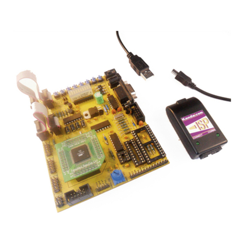
KANDA STK300 User manual

Page 1
STK300 USER MANUAL
Published by
KANDA SYSTEMS LTD.
www.kanda.com

Page 2
STK300 User Manual
Copyright © Kanda Systems Ltd. 1999.
All information contained in this publication, including product data, diagrams and
charts, represent information on products at the time of publication, and are subject to
change by Kanda Systems Ltd. without notice due to product improvements or other
reasons.
Kanda Systems Ltd. assumes no liability for the accuracy or use of the information.
Kanda Systems Ltd. assumes no responsibility for any damage, or infringement of any
third-party’s rights, originating in the use of any product data, diagrams, charts or
circuit application examples contained in this publication.
All copyright and trademarks are recognized and are the property of their owners.
No part of this publication may be reproduced or distributed in any form or by any
means, or stored in a database or retrieval systems, without the prior written
permission of Kanda Systems Ltd., except in the case of brief quotations embodied in
critical articles and reviews.
© Copyright 1999 Kanda Systems Ltd. all rights reserved.
Version 1
Kanda Systems Ltd.
Unit 17/18
Glanyrafon Enterprise Park
Aberystwyth
Ceredigion
SY23 3JQ
UK

Page 3
Introduction
Welcome to the Kanda 300 Development Kit.
This system incorporates an In System Programming unit and an applications board.
For late breaking news and any manual errata always check the README.TXT file included with
the software.
Device Support
The system software currently has support for the following devices.
•AVRMEGA103
•AVRMEGA103L
•AVRMEGA603
•AVRMEGA603L
Upgrades for new devices will be available via the Internet from www.kanda.com
Kanda Systems cannot be held responsible for any errors or omissions in this system. The limit
of any liabilities is limited to providing replacement hardware or software.

Page 4
Getting Started
Unpacking the system
You will find the following items in the box:
•Main Board
•1 Disk set
•ISP Dongle
•ISP Ribbon Cable
System Requirements
The minimum hardware and software requirements are:
•80386 processor or above (486 or above recommended)
•1MB RAM
•1MB free hard disk space
•Windows 95/98/NT

Page 5
Connecting the system
On/Off
Switch Power
Connector
RS232
Connector Programming
Interface
Port Headers
A power supply is required with a standard 2.1mm barrel connector. It can be AC (7 - 12 V) or
DC (9 - 15 V). The connector is inserted into the power connection socket as shown.
The programming lead supplied is fitted into the Dongle case and the other end is inserted into the
programming interface on the board as shown.
The Dongle case is connected to one of the printer ports on the PC. If this is not LPT1, then you
will need to change the printer port setting in the software - see software section for details.
Connect Lead supplied
to Dongle and insert in
PC Printer Port or
Serial Port
RS 232 Connector
Not used for
programming
Power Connector
5.5/2.1 Barrel
On-Off Switch
Plug header on
lead into
Programming
Interface - Key way
gives orientation
Power Supply
9 - 15 V DC
7 - 12V AC

Page 6
Hardware Description
The main features of the board are shown in the diagram below.
Note: There are a number of jumpers on the board which are used to select different operations
and voltages. The default jumper settings are for programming operations at 5V (JP1 Closed)
with brownout also set to 5V (JP2 Open).
To carry out other operations, some jumpers may have to be removed - refer to the relevant
section for details. A full list of the jumpers and links are given in the table overleaf.
Plug in MEGA
board here
Analog I/P
Port A Digital
Port B Header
Port C
Header
Port D Jumpers
Disable Switches
Port D
Header
Misc Header for
non-port pins
8 switches on Port D
8 LEDs on Port B
JP2 for Brown-out
at 3.3V or 5V
On-Off
Switch
Power Input
9-15V DC or
7-12V AC
ISP Interface
Ext. SRAM
Address Latch
IC for RAM
4MHz Crystal
LCD
Contrast
Adjustment
LCD Connector
Analog Reference
Voltage Adjustment
Port B
Jumpers
Disable LEDs
JP1 Jumper for 3.3
or 5V Vcc Select
LK1 - Cut for A/D
External Reference
Power On
and Program
lights
Selector for
RS232
External
Memory
Expansion
Port E Header
O/P pins for
Ve supply to
Op-Amp etc.

Page 7
Jumpers and links and their functions
Jumper Function Open Closed Default
JP1 Voltage select 5v 3.3V Open
JP2 Brown out select 2.9V 4.5V Closed
PE0 RS232 RXD Port E.0 RXD Port E.0
PE1 RS232 TXD Port E.1 TXD Port E.1
Port B LEDs LEDs Disabled LEDs Enabled Closed
Port D Switches Switches Disabled Switches Enabled Closed
LK1 Analogue
Reference if LK1 cut then
EXTERNAL REF
from header
ONBOARD POT Closed
CUT Under
Board LCD Contrast If Cut, add extra
resistor Contrast Pot Closed
External Connections
All Ports are brought out to edge of board on to headers. Each header has a Vcc and Ground pin
for power supply to external circuits. Port F is the Analog input port and is on a header marked
Analog. There is an extra six-pin header for miscellaneous functions - Read, Write, ALE, Reset,
Ground and Vcc.
See sections on Using External Connections and Using Analog Functions for details.

Page 8
Installing The Software
Windows 95/98/NT
To install the software please insert the supplied disk or CDROM in your computer and perform
the following steps:
•Click on your Start button.
•Select Settings.
•Select Control Panel
•Choose Add/Remove Programs.
•Click the Install button.
•Follow On-Screen prompts.
The software will then be installed onto your computer and an Icon will be added to your start
menu.
Note: On some PCs, especially laptops, programming problems may occur if the Bios Parallel
Port settings are set to EPP Version 1.7. If programming problems do happen, ensure that the
Parallel Port settings in your BIOS are set to EPP V1.9 not V1.7.
This software does not run on Windows 3.xx.
Note: If you have any problems installing the software or suspect that you have faulty media
please contact our technical support department. Please make sure you have the latest version of
the software installed before contacting the support line.
Telephone: +44 (0) 1970 621041
Fax: +44 (0) 1970 621040
E-mail: [email protected]
Website www.kanda.com

Page 9
How to use the Software
The Programmer software is shown below:
Overview
The programmer uses three main displays:
•Flash Memory
•EEPROM Memory
•Status
Data and information is displayed on three screens. You can access each screen with a click on
the relevant button or via the View menu.
The main menu details file and programmer operations and the configuration information is shown
just below the menu bar.
A status indicator at the bottom of the screen shows whether an operation was successful. A red
light indicates an error has occurred.
Status Indictor and
Message Line
Red = Error
Yellow = In Progress
Green = OK
Memory Buffer
Window
- Editable
ASCII Pane
- Editable
Window
Selection Main Menu Device
Selection Security
Settings Hardware
Selection

Page 10
Configuring the software
1. The first step is to choose the type of hardware connection, using the drop-down list at the top
right of the screen. Select E-ISP Serial Port or E-ISP Parallel Port as required. Ensure that
the board is connected to the serial or parallel port as appropriate.
2. Select the required device in the Device drop-down. The memory sizes, fuse availability and
other device specific features are set automatically to fit the selected device.
3. Select the Programmer - Options menu choice.
Tab Type of
port Description
Port
selection Parallel Select from LPT1, LPT2, and LPT3
Serial COM 1, COM 2, COM3 and COM 4
Advanced
options Parallel Maximum Read and Write Timeout settings with a default
of 180000 and minimum Baud rate.
Serial Maximum Read and Write Timeout settings with a default
of 100000.
Note: If you have Time Out Errors when using the programmer you should try and
increase the time outs.
Voltage Serial and
Parallel Sets the operating voltage. Select the required level of Vcc
(Vdd). Most programming operations are at 5v even if the
voltage is set differently. Check the Atmel datasheets for
voltages that can be used on the ports. Note: Some low
voltage parts need 5V for programming.
The selected voltage is applied as soon as the dialog is
closed. It will change to 5V as soon as programming
operations takes place. Selecting Device, Run will re-
apply the operating voltage selected.
4. Select the level of programming security required from the Security drop-down menu.
Note: Some Tiny AVR devices, especially early versions, can lock out after the security lock bits
are set. Apply the lock bits after the code has been developed.
Loading Data
1. Select File - Load. A sub- menu enables you to select Flash or EEPROM Memory as the
target for the load operation.
Note: Only INTEL hex files can be used.
2. Select the appropriate file.
Status light Description
Red Error during the load operation, because:
•the file can not be found
•the file is not INTEL Hex,
•the file is too big
•or any other error
Error message displayed. Click on Error message to view Status window.
Green Operation successful

Page 11
Yellow Operation is taking place
This light coding applies for all operations.
3. When a file has been loaded into the Flash memory and the EEPROM memory if required, the
programmer is ready for programming operations. EEPROM data (or Flash data) can be
typed directly into the buffer windows instead of being loaded from a file. The data can be
entered as ASCII characters or as Hexadecimal numbers.
Programming
The programming operations are listed in the Device menu. The programmer must be configured
before programming can be undertaken, and for the Program function, data must be loaded into
the buffer windows
The options listed in the Device menu are:
Option Description
Erase The device is erased and code and EEPROM memories will be empty - blank
value is FFh. All Fuse settings will be cleared to default values (see data
book/CD-ROM for device specific fuse information).
Program Choose Flash, EEPROM, Lock bits or Fuses on the fly-out menu. If Flash or
EEPROM is chosen, then that part of the device is programmed with the
contents of the Flash or EEPROM buffer window respectively. If lock bits are
selected, the security bits are programmed according to the Security Settings
drop-down list described above. If Fuses are chosen, a dialog box appears with
the fuses available on the selected device. Set the fuses to your requirements.
Read If Flash or EEPROM are selected, the contents of the device memory selected is
uploaded and displayed in the relevant buffer window. If the device is blank,
then all locations will read as FFh. If the security (lock) bits are set, then the
data will be invalid. Selecting Fuses displays the status of the fuses on the
selected device in a list box.
Verify The contents of the selected memory area (Flash or EEPROM) on the device is
compared with the contents of the equivalent buffer window and any differences
are shown in Red - correct values are shown in Green.
Fuses Only available with some devices. Used for such functions as clock selection,
etc. You can read or write to the fuses of the selected device.
Run Converts the board operation to run mode. The operating voltage selected
earlier comes into effect.
Auto Program will run all, or a selection of the above options.
Select Auto-Program Options to set the required programming operations. A list of operations is
displayed:

Page 12
Check the required functions. All the selected functions will run when Auto-Program (F5) is used.
If Program Fuses is available and checked, then another dialog box will appear after this list is
closed where you can set device specific fuses.
Note: Erase the device before programming unless you are adding extra data to existing data in
the device. If you are changing data then you cannot change any programmed bit from a 0 to a 1
without erasing the device first. You can however, change a bit from a 1 to a 0. So BB could be
changed to AA for example but AA cannot be changed to BB. You will not be able to program the
device if the write lockbit has been set.
Warning: Setting Lockbits may mean that you will be unable to perform further verification on the
device, and disable further writing to the device, You will be able to re-use the device if you
perform an erase.

Page 13
Menu and Option Descriptions
File Menu
Load Select memory area/buffer window to load (Flash or EEPROM), then
open the Intel Hex file in the Open File dialog box. A red status
warning light indicates that the file load was unsuccessful. This may
be because the file is not Intel Hex or it is too large for the selected
buffer/memory.
Save Saves the contents of the buffer selected (Flash or EEPROM) to file.
Choose a filename in the File Save dialog box that appears.
Reload Reloads the buffer (Flash or EEPROM) with the last file opened.
Exit Quits the program. Standard Windows close choices can also be used
to exit the program.
Device Menu
Erase The whole device is erased.
Program The selected device memory, fuses or lock bits are programmed
Read The selected device memory or fuses are read
Verify The selected device memory is verified against the buffer contents
Fuses This is available if the software and device support this function
Run Runs the program downloaded to the device on the board.
Auto Program All operations selected in the Auto Program Options are carried out
Auto Program
Options Dialog box to set required programming operations that will be carried
out sequentially when Auto Program is pressed.
Programmer Menu
Options Dialog box for port selection, read/write timeouts and voltages (1.8 -
5V). You must choose Parallel or Serial port operation and the correct
device first. Note: Most parts program at 5V even if they are low
voltages for operation.
Information Shows information about the programmer state e.g. hardware
detected, which port etc.
View Menu
Flash The Flash Memory Buffer window is displayed.
EEPROM The EEPROM Memory Buffer window is displayed.
Status The Status Window is displayed. This lists all operations, error
messages, and status information that have been posted during this
session.
See also Window selection on the next page.
Help Menu
Readme Displays the latest information on the software and devices in the
Status window.
About Version and Program information

Page 14
Other Controls
Device Selector
Located at the top left of the screen, this drop-down list is used to select the required device.
Make sure that this selection matches the device you have plugged into the board. Obtain an
upgrade to support new devices as they are released.
Security
Located in the center of the screen, Security is used to select type of access to the device once it
has been programmed. This is done by programming the lock bits, so ensure that the lock bits
are checked in the Device, Auto Program Options if you want security set on the device, or
select Device, Program, Security Lock bits for manual programming.
Hardware Selection
Located at the top right of the screen, the hardware selection must be set to either serial or
parallel port. Which serial or parallel port is used is set in the Programmer, Options menu.
Ensure that the board is connected to the correct port.
Window Selection
Located below the Device field, these three buttons indicate which display is visible.
•Flash buffer window
•EEPROM buffer window
•Status Window
See below for details. Which display is active can also be selected using the View menu. See
previous page.
•Flash Memory
Displays the Flash memory in a buffer window.
The code to be programmed into the device is loaded into this buffer by the File, Load,
Flash option, or read from the device by the Device, Read, Flash option.
The size of the buffer changes to mirror the Flash memory size on the selected device. If
Device, Verify, Flash is used, the contents of this buffer are compared with the contents of
the Flash (code) memory on the device.
Locations which match are shown in green, mis-matches are shown in red. The data in this
buffer window can be changed or entered as either hexadecimal numbers or ASCII
characters. Holding the mouse cursor over a value brings up a fly-out, which gives the
address and the value in decimal, binary, hexadecimal and ASCII.
•EEPROM Buffer
Displays the EEPROM memory in a buffer window.
The code to be programmed into the device is loaded into this buffer by the File, Load,
EEPROM option, or read from the device by the Device - Read - EEPROM option. The size
of the buffer changes to mirror the EEPROM memory size on the selected device.
If Device, Verify, EEPROM is used, the contents of this buffer are compared with the
contents of the EEPROM memory on the device. Locations which matches are shown in
green, mis-matches are shown in red. The data in this buffer window can be changed or
entered as either hexadecimal numbers or ASCII characters. Holding the mouse cursor over
a value brings up a fly-out, which gives the address and the value in decimal, binary,
hexadecimal and ASCII.

Page 15
•Status
This window lists all the operations, status and error messages that have occurred
during the current session. To clear the messages displayed, right-click and select
Clear Status.
Status Indicator
Displays a visual result of the current operation - Red means that the operation failed, Yellow
means it is in progress and Green means it was successful. Further information is given in the
accompanying message. These messages are listed in the Status window.

Page 16
Programming Using the Board
Device Orientation
Before programming a device using the programming module, the device adapter must be
inserted correctly into the programming unit. The adapter itself has a corner cut off, which locates
pin 1 of the device and matches the marking on the main unit. This adapter should be pre-fitted,
but can be replaced if the device programming life is exceeded - refer to your supplier to obtain
new device adapter.
The orientation of the device is vitally important. If you put it in the wrong way then you may
damage the device. DO NOT PLUG A DEVICE ADAPTER IN WITH THE POWER SWITCHED
ON or you may damage it. Similarly never remove the device adapter with the power on.
Voltage Selection
Jumper JP1 is used to select either 3.3V or 5V programming.
For Vcc = 5V remove jumper JP1 - jumper open
For Vcc = 3.3V insert JP1 - jumper closed
Jumper JP2 is used to set Brown-out detector voltage.
For Brown Out = 5V insert jumper JP2 - jumper closed
For Brown Out = 3.3V remove jumper JP2 - jumper open
This should be set to the same voltage as Vcc. If Vcc is set to 3.3V and Brown-out is set to 5V,
then the device will be held in reset and will NOT program. See section on Brown-out Detector for
more details.
JP1
JP2
Power and Lead Connections
The 10 way programming lead is inserted in the box header - the key-way ensures correct
orientation. The computer connections are shown in the section on Connecting the System.
The power supply (9-15V DC or 7-12V AC) is plugged into the power connector (5.5/2.1 Barrel).
The Power ON/Off switch is located next to the power connector. Insert the device adapter before
switching the power on. The power on LED should light when the power is correctly applied.
Your hardware is now ready for programming. Refer to Using the Software description for details
of programming operations. A programming LED indicates programming is happening.

Page 17
Brown Out Detector
The brown out detector circuit is used to detect voltage drops. If a short glitch occurs in the
power, this circuit ensures that the processor resets properly rather than operating randomly.
The brown out detector must be set to the same voltage as the circuit voltage (Vcc) - 3.3V or 5V.
For 3.3V operation, jumper JP2 must be removed (jumper open) and for 5V operation it must be
closed.
Voltage Operating Voltage Hysterisis
5 Volts 4.5 Volts 200 mV
3.3 Volts 2.9 Volts 200 mV
These values are approximate and may vary with temperature and other factors.

Page 18
Board Applications
Using Switches and LEDs
The LEDs are connected through a 1K resistor network to Port B.
The switches are connected to Port D.
The switches and LEDs can be disconnected if required, so to use them, ensure that the jumpers
labeled Port B and Port D are closed. The board is also marked with the port pin connection for
each switch and LED.
The ports must be correctly set in software as input or output. This is accomplished by setting the
direction control registers to 0 for input and 1 for output. Typical set up code would be :
mov r16, $ff ; move literal into temporary store register
out DDRB, r16 ; set direction register to ones for output - LEDs
out PORTB, r16 ; switch all the LEDs on
mov r16, $00 ; move literal into temporary store register
out DDRD, r16 ; set direction register to zeros for input - Switches
Using External Connections
•All the ports are brought out to headers on the edge of the board. In addition to the port pins,
each header has a connection for ground and Vcc to supply external circuits. Note this
voltage (Vcc) will be either 3.3V or 5V depending on the setting of jumper 1 (JP1) and the
brown out detector will operate.
Note : If your circuit is to draw significant current ( >250 mA) then a heat sink will be required on
the on-board regulator - LM317. This device is rated at 1.5 Amps but it does need a heat sink to
supply this current. If your circuit will draw more than 1 amp, you may need a separate power
supply. The ports on the device are connected to the headers marked Port A, Port B, Port C, Port
D, Port E and Analog (Port F). The layout of all the headers is the same and is shown in the
diagram.
BIT 1
BIT 3
BIT 5
BIT 7
Vcc
BIT 0
BIT 2
BIT 4
BIT 6
GND
Misc Header
Bit 0 of Port. Same
for all Ports.
Cut Corner shown on
board for orientation
Bit 7 of Port. Same
for all Ports
Extra Connection
for Vcc
Extra Connection
for Ground

Page 19
The last header labeled Misc has connections to processor pins other than the port pins.
ALE
EXTERNAL
RESET
Vcc
Read
RD
GND
Write
WR
If external operations do not want pull-ups on the port pin, both the switches and the LEDs can be
disconnected from the processor. To isolate the LEDs, remove the jumper set labeled Port B, and
to isolate the switches, remove the jumper set labeled Port D.
Using Analog Functions
The A2D converters use the header labeled Analog for the A/D inputs on Port F, which is input
only. A +10V to -10V supply is provided on the connector marked Op-Amp next to the crystal. A
lead from this connector can be used for an external amplifier for the ADC inputs. The layout of
the Analog header is shown below.
Analog Port : Marked on Board
ADC1
ADC3
ADC5
ADC7
ANALOG
REF
ADC0
ADC2
ADC4
ADC6
ANALOG
GND
The A/D converters can use either the on-board (Internal) Voltage Reference or an external
Voltage Reference.
Cut out marked on
board to give
orientation
Extra Connection for
Vcc
Extra Connection for
Ground
Cut out marked on
board to give
orientation
ADC0 - ADC7 connected to Port F PF0 - PF7

Page 20
Using Internal Reference
To use the internal (on-board) Voltage Reference, the pot marked AREF is used to set the voltage
level. The voltage level can be measured with a meter connected to the header pins labeled
Analog Ref and Analog Gnd in the above diagram or from the two holes marked Meter (+ and -).
Using External Reference
To use the A2D converters with an external Voltage Reference, the link marked LK1 must be cut.
The voltage is applied to the pins marked Analog Ref and Analog Gnd on the Analog header - see
diagram above.
Dual Rail Power Supply
An dual rail power supply is included - marked OP-AMP. It is design to provide a low current
(<2mA) supply for external operational amplifiers for signal conditioning etc. on the ADC inputs. It
is designed to supply +10V and -10V, but this may vary especially if the RS232 is being used.
Using Real Time Clock
A 32768 Hz crystal is connected to TOSC1 and TOSC2 pins - Pin 19 and Pin 18. This can be
used to generate a 1 second pulse by setting Timer 0 to Asynchronous Operation - see data book
for details.
Using External RAM
The AT90MEG103 can be used with external SRAM. A socket is provided for a 28 pin RAM chip
and for an address latch chip. These are next to the device adapter at the top of the board. There
is also a header for further memory expansion, which is connected through the address latch.
The pin functions are marked on the board, including chip select (CS).
RAM recommendations
A low power 62256 SRAM is suggested with an access time of 70 nS. If a very fast RAM is
required, the crystal frequency may need to be increased. If a much slower SRAM is used, the
SRAM Wait State bit must be enabled in user software (see data book). The layout of the 28 pin
RAM socket is shown below, and any RAM with this pin-out could be used.
The RAM is memory mapped to $8000..$FFFF.
Other manuals for STK300
1
Table of contents
Other KANDA Microcontroller manuals
Popular Microcontroller manuals by other brands

InterNiche Technologies
InterNiche Technologies PIC32MX user guide

Samsung
Samsung ARTIK 530s manual

Silicon Laboratories
Silicon Laboratories C8051F00 DK Series user guide

Atmel
Atmel ATmega645 Application note

Abov
Abov MC80F0304 user manual

NXP Semiconductors
NXP Semiconductors LPC5411 Series Product data sheet