KD1JV Designs Mountain Topper User manual

The Mountain Topper
Tri-bander
(revised 4-10-14)
A very small, very efficient, three band rig
By
KD1J Designs
580 Durand Rd
Randolph, NH 03593
http://kd1jv.qrpradio.com stev[email protected]
Specifications:
Three bands, choose 3 - 40M, 30M, 20M or 17M.
80M possible, but filter parts not supplied.
Receiver:
MDS: ~0.2 u
Small signal band width ~ 500 Hz
Audio output limited to ~ 1200 mv p-p
Headphone output, 16 ohms min recommended.
Minimum current (no signal) ~40 ma
Transmitter:
2.5 watts @ 9 volt supply typical
Spurs -50 dBc or better
Table of Contents
Assembly:......................................................................2
Check out and Calibration:...........................................13
Reference Oscillator Frequency Calibration:....13
Local Oscillator frequency trim and FO
adjustment:........................................................14
FO adjustment: ..............................................14
Receiver input peaking:.....................................14
Transmitter test and output (low pass) filter
adjustment:........................................................14
asic operation:...........................................................18
Turning the rig on and off:.......................................18
and selection:.......................................................18
Volume control: ......................................................18
Input attenuator:......................................................18
Control switches:....................................................19
Frequency tuning: ..................................................19
Tuning limits: .....................................................19
RIT:.........................................................................19
MENU:....................................................................20
Quick selections: ....................................................20
DFE Mode: .......................................................20
Tune Mode: .......................................................20
attery Voltage:.................................................21
Fn switch only selected functions:..........................21
Frequency readout: ................................................21
S: Selecting Keyer code speed..........................21
M: Keyer Memory entry: ..................................21
Checking and storing the message:...................22
Sending messages: ..........................................22
eacon Mode:...................................................22
P: Program user preferences.............................23
Straight key mode:..................................................23
Operating voltages: ................................................23
HIGH SWR CAUTION: .....................................23
1

Assembly:
●Your work area should be reasonably clean and uncluttered. Good lighting is a must.
●Empty the packets containing the parts into small paper bowls. This will ensure that they do not get
lost. Some people like to do the assembly over a cookie sheet as the lip around the edge helps to keep
parts from going far. The metal sheet also provides some measure of static control, especially if you
ground it. A white sheet under your work area could help in finding a part which might get away from you.
●A very thin 0.015”) solder is supplied for soldering the surface mounted parts. Very little solder is
need for each connection. Ideally, you want a little convex fillet at the end of chip resistors and
capacitors. Try not to end up will a ball of solder at the end of the part.
●Do not use liquid solder flux. It simply makes a mess and is difficult to clean off the board and get out
from under parts. If not completely removed from the board, it can cause problems.
●Before placing a part, lightly tin one pad for where it will go. You can speed assembly by tining one pad
at all the locations for which a particular value of part will go. There is no need for a low wattage
soldering iron. It is best to have a hot tip which will let you get the job done quickly. You will need
a small tip on the iron, 1/32” to 1/16” chisel or round is best.
●Most of the surface mount parts come in part carriers. To remove the part s), hold the carrier close to
the work surface and carefully peel back the clear plastic covering the part. This can be done with the
tip of a sharp hobby knife such as a #11 Xacto blade or pointy tipped tweezers. Once you remove the
clear plastic strip, dump the part out of the carrier and onto your work surface.
●If you use tweezers to handle the parts, be very careful you don't grab onto them too tightly. These
little parts have a way of flying out from between the tips of the tweezers, never to be seen again.
Apparently, they go into the twilight zone, along with all the pens, small parts and hardware which
falls off the bench. They must go someplace since its never anywhere I can ever find them again!
●An alternative to using tweezers to handle the parts is to use a tooth pick or chop stick with the end
rubbed into a little bees wax. The bees wax makes the end sticky so the part will stick to it. For the
smaller IC's I grab them length wise with the tweezers.
●Tack the end of a part in its place by applying heat to the end of the part over the tined circuit board
pad, while applying a little pressure to make sure it lays flat to the board. Be sure to heat both the
pad and the end of the part. Generally, you will not have to add any additional solder to this
connection. Then solder the other end of the part. If you don't do this right away and go onto tacking
down some more parts, there is a good chance you will forget to go back and solder all the parts which
require it.
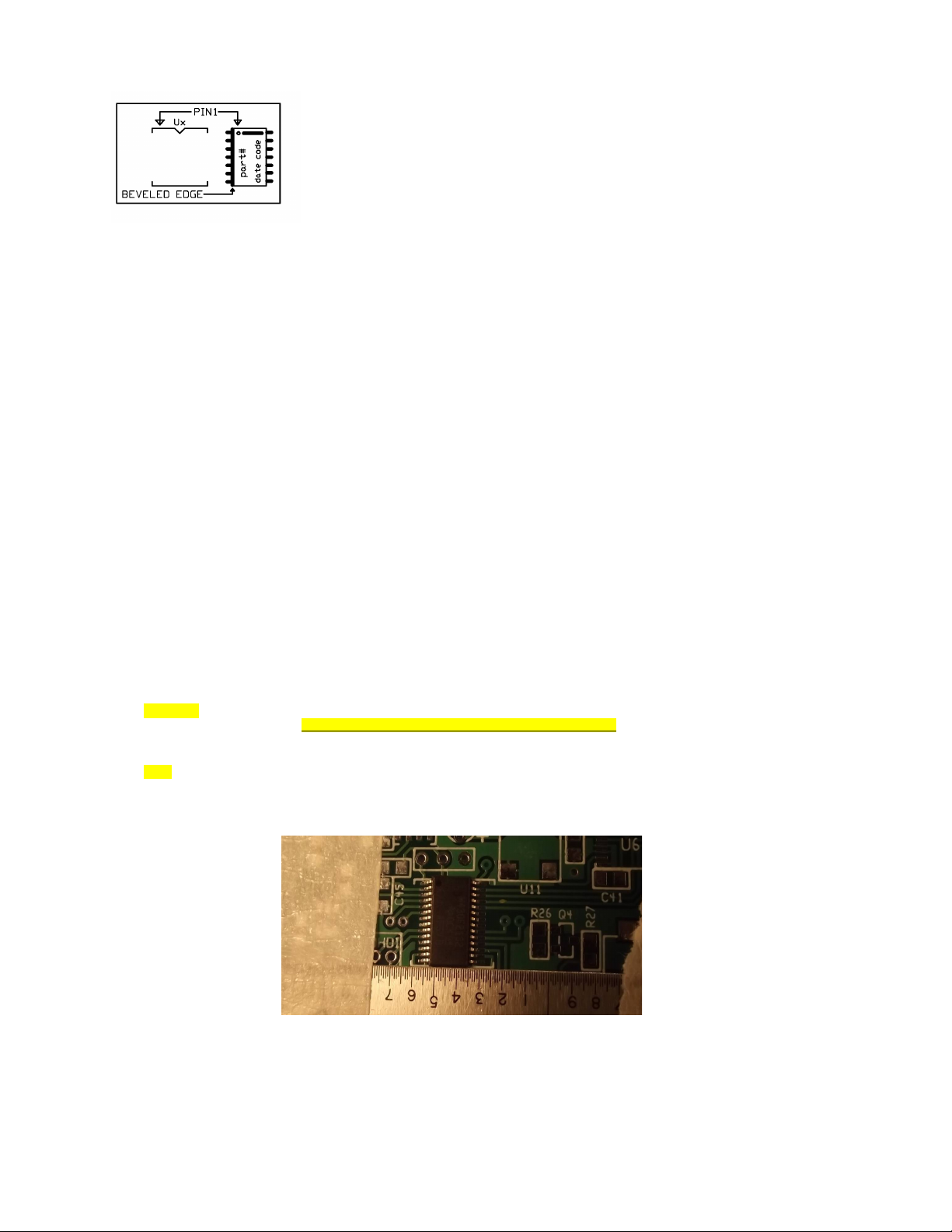
●It is nearly impossible not to make solder shorts between pins on the DDS chip, due to the close pin
spacing. Remove any shorts with solder wick.
Using solder paste:
Using solder paste is the ideal way to build the board. Small amounts of solder paste in an application syringe
can be bought for about $5.00 from Cash Olson over the internet. Also needed is a warming plate to preheat the
board to about 200 degrees and a low power heat gun. An “Embossing” heat gun is commonly used found at craft
stores), though a hair dryer on low setting might work. A soft air flow is required as to not to blow parts off
the board.
For chip caps and resistors, a very small dab of solder paste is put on the pads and then the part placed
over the pads. The parts will slide around very easily, so one must be careful not to nudge them. For IC's,
placing the IC down first, then putting a bead of paste along the leads looks to be a better method then putting
the paste on the pads first, then the IC.
The LED display should be hand soldered, along with all the through hole parts. Start with the side of the board
with the most parts first bottom in the case of the MTR).
Once all the parts have been placed, put the board on the warming plate and heat to about 200 degrees.
Then slowly heat the top of the board with the hot air gun. When the solder paste reaches its melting point, you
will see it liquefy and the parts snap into alignment to the pad. This is when the solder paste turns from a dull
gray to shinny. Be on the look out for “tomb stoning” which is when a chip cap or resistor will stand up on one
end. Once all the solder has reflowed, remove the power to the heating plate and let it cool down.
I have a youtube video showing how to solder SMT parts, both by hand and using solder paste.
http://youtu.be/Ah5HEjDTHUo You may want to watch some of the other suggested videos on SMT soldering which are
done a bit more professionally then mine.
2

Using the parts placement guides:
The parts placement guides on the following pages are color coded to show the location of the various types of
parts. Parts to be installed are highlighted in various colors to help identify their locations. The guides are
scaled so that the writing on them is easy to see on a computer monitor and come out crisper after the conversion
to pdf. Unfortunately, if you print all these pages out, it will use up a bunch of your ink jet ink.
Some parts do not have values marked on them or are very hard to read. Capacitors are not marked so these have
been color coded with a marker on the part carrier using the resistor color code to indicate their value in pfd.
SOT-23 parts have numbers printed on them, but are very hard to read. Therefore, these parts are also color
coded, but with a color sticker, as they come in plastic carriers. The color on the carrier matches the color
shown on the placement guide diagram.
Resistors have their value printed on them, though it might take a magnifying glass to read the numbers.
Therefore, individual values are not color coded.
Here's what the finished board should look like when your done:
I made the mistake of using hot air to attach the LED display and ended up melting the bottom edge. Therefore, if
you use solder paste, hand solder the display.
3

Component location diagrams
These diagrams show the overall part locations and values. This page can be printed out to help locate part
locations.
Color highlighting is used to help identify component type, not value. Blue = capacitors, Yellow = resistors,
Red and orange = inductors, gray = semiconductors or through hole parts.
Top Side:
Bottom Side:
4

Parts list:
5
QTY Value Color code or value #
1 or
2
51 510 The extra 51 or 270 resistor
used to select 17M band
option.
3 or
4
270 271 50-50 chance of getting the
51 or 270 resistor.
9 470 471
2 2.2 K 222
1 3.9 K 392
7 10 K 103
5 22 K 223
3 100K 104
1 330K 334
1 2.67K 2671 1%
1 14.0K 1402 1%
1 113K 1133 1%
1 267K 2673 1%
7 30 p Trimmer caps
3 3.3 p (3.3) GRN/GRN
5 22 p (22) RED/RED
1 33p (33) Org/Org/ lk
2 47 p (47) YEL/VOL
2 68 p (68) LU/GRY
8 100 p (101) RN/ LK/ RN
11 1000p (102) RN/ LK/RED I accidentally cut a bunch
of strips of 10, so some kits
have one of these caps
loose.
15 0.01 u (103) RN/ LK/ORG
1 0.022u (223) RED/RED/ORG
7 0.1 u (104) RN/ LK/YEL
1 1 u (106) RN/ LK/ LU
2 4.7 u ELECTRO
1 33 u ELECTRO
1 100 u ELECTRO
2 3.9 uH RED L3, L6 SMT 1206
3 10 uH LUE L1, L2, L11 SMT
0805
2 22 uH 40M RED/RED/ LK/GLD
2 12 uH 30M RN/RED/ LK/GLD
2 8.2 uH 20M GRY/RED/GLD/GLD
2 100 p (101) C0G leaded
2 150 p (151) C0G
3 220 p (221) C0G
3 330 p (331) C0G
1 560 p (561) C0G
1 680 p (681) C0G
QTY Part number Color code or
value #
location/description
2 SA612A U1, U4 MIXER
1 LM4808M U3 AUDIO AMP
1 TC1014-3.3VCT713 lue A5xx
(last two
characters
are date code
U6 3.3V REG
1 LM386M U2 AUDIO AMP
1 AD9834 RUZ U8 DDS
1 MCP1703-5002E/D MCP1703 U7 5V REG
1 74AC02M AC02 U9 QUAD OR
1SN74LVC1G3157D V CC5x U5 ANG SWITCH
1 MSP430F2132IPW U10 MPU
1 ASV-50-EJ-T ASV 50.0 U11 50 MHz CLK
2 2N7002 RED [702] Q1, Q2 MOSFET
2 NDT2955 2955 Q3, Q5 P-CH
3 S170 Q4,6,7 MOSFET
1 AV99 YEL [A7] D1
2 ZT52C5V1-F [W8] D2, D3 5.1V zener
1 ZX85C47 GLASS D4 47V zener
1 0.3” 7 SEG LED DISPLAY
1 32.768 kHz CYLINER CRYSTAL
5 4.9152 MHz HC-49/US XTAL, MATCHED
1 DPDT Slide switch
3 DP3T SLIDE SWITCHES
4 6 X 4.3mm TACT SWITCH 612-
TL1105EF100Q
1 1.7mm X 4mm DC JACK 163-4018-EX
1 1.7mm X 4mm DC PLUG 171-3219-EX
2 3.5mm STEREO JACKS
4 0.187” # 2 SWAG THREADED SPACER
4 #2-32 SCREWS
1 Red display filter film
6 T-30-2 RED IRON TOROID
1 FT37-43 LACK FERRITE TORIOD
1 8+ feet #28
MAGNET
WIRE
1 1 feet HOOK UP WIRE
1 48” 0.015” SOLDER
1 CIRCUIT OARD
4 umper feet
1 3” solder wick
1 Enclosure, top and
bottom.

Semiconductor placement
●Finding Pin 1. Some of the ICs used in this kit have a dot or
indentation at the Pin 1 corner of the chip. For others, the Pin 1
locations isn't as obvious. The manufactures logo is sometimes used as
is the case for U1 and U3) or sometimes there is a line along the Pin 1
end of the chip. In all cases, there is a beveled or rounded edge along
the side of the Pin 1 left) side of the IC package. When the package is
orientated vertically and the beveled edge is to the left, Pin 1 is
always in the upper left corner as shown in the diagram.
●U1 and U4, SA612) use the manufactures log NXP) for the pin 1 corner designator.
●Before placing an IC or transistor, tin one of the corner pads and then tack that lead of the part down
first. Before soldering any other pins, make sure all the leads are lined up on the pads. This is
especially important for U8 and U10, where these isn't much room for error. see hit below for an aid to
lining up the leads with the pads) Then solder the lead on the opposite corner from the tacked lead to
make sure the body doesn't move when you solder the rest of the leads.
●You will have to carefully check the number on the 8 pins IC's to tell them apart. Using a magnifying
glass and tilting the part slightly to the light will aid in reading the a part number. The rest of the
IC's are each in unique packages, so are easier to determine their locations.
●Tilting an IC to the light can make reading the part number easier.
●U5 and U6 are very similar. The way to tell them apart is the fact U5 has 6 leads and U6 has 5. To help
tell them apart, the U6 part carrier has a Blue sticker on it. U5 has a faint dot which marks the pin 1
end, also the lettering “CC5R” will be upside down when installed correctly.
●There are several different SOT-23 devices, the packages they are in are each color coded to match the
layout diagram.
●U11 is the rectangular box with the silver top. Be sure to get solder to flow into the little “U” shaped
cups near each corner of the part. A number of builders have had trouble with this and not made solder
connection to the pads under the part. A fine tipped iron is required here. Also, be careful of using
too much solder and making a short to the metal top of the package.
●D3 has very faint line on one end to indicate the cathode end. Look carefully for this line and face it
towards the line printed on the board.
●There maybe more numbers or letters on the semiconductor packages then indicated on the layout diagram.
These are date or lot codes and can vary depending on when the parts are purchased. Therefore these are
not used for part identification on the layout diagrams.
●CAUTION! There are three parts in SOT-223 packages, one of which is the 5V regulator, which goes on the
top side of the board. Do not mix up with the 2955 MOSFETS, Q2 and Q3. The regulator is loose in the
semiconductor parts bag, while the two MOSFETS are together in a parts carrier.
●HINT: Taping a straight edge, such as a thin metal ruler, across the board and lined up with the bottom
outline of U8 or U10 as the case maybe) will aid in keeping the part aligned with the pads. First do U8,
then U10. After soldering the leads, clean up any solder shorts with the supplied solder wick. Be sure to
only pull the wick parallel to the leads, not against the gain!
6

Bottom side semiconductors:
NOTE: The lettering on U5 and U6 will be “up side down” when viewed with
this board ordination. Note the faint DOT indicating pin one on U5 and
the corresponding dot on the board. Look very carefully for the line on
the D3 diode indicating the cathode end.
Whether you use solder paste or hand solder, you will likely have shorts between the leads of U10 and U8. Use the
supplied solder wick to remove the shorts. Place the wick over the leads and apply heat with your iron. Be sure
to slide the wick off the pins along the leads, not across them.
U11: make sure you get the clock oscillator positioned correctly. Once soldered in place, it is very difficult to
remove. Also make sure you solder it well. Not making good connections to the little solder tab cups on the side
of the part has been a problem for some, likely due to have a soldering iron tip which is a little too big.
7
LOCATION PART # PACKAGE
U8 AD9834 TSSOP-20
U10 F2132 TSSOP-28
Q2 Red/702 SOT-23
D1 Yellow /A7 SOT-23
U1/U4 SA612A SO-8
U2 LM386 S0-8
U3 LM4808 SO-8
U9 74AC02 SO-14
D3 -- W8 2 leads
U6 lue/A5xx SOT23-5
U5 ---- CC5x SOT-23-6
U11 50.00 silver
Q3 2955 SOT-223
Remember, Q3 is in parts carrier, not loose
The last letter on U5 is a date code.

Resistors : Bottom
●Since part designation numbers for most parts are not printed on the board, you will need to use the
diagram to locate where the part goes. Pay careful attention to where the part is located to be sure it
doesn't go where a cap will go later.
●Resistor locations are highlighted in yellow. The number shown inside the outline is the same as marked
on body of part. Note that several resistors have four numbers printed on them, these a 1% values.
Resistors with three digits are 5%.
●Three inductors will also be installed with the resistors. These are packaged with the resistors, but are
larger and have no numbers printed on them. There are two values used, so they are color coded. The two
left over “orange” inductors will be used on the other side.
●There will be a number of resistors left over which go on the top side of the board. Put these aside in a
safe place until needed.
●The “approximate location ” in the table will help locate the position of the resistor values on the
board. upper/middle/lower is Y coordinates area while left/center/right is X coordinates.
●Resistors R1, R2 and R3 values depend on the band to be used see band value table below. The placement
diagram shows the location and values for the typical 40/30/20 band line up. You might decided to make
you band selection 40/20/17 or 30/20/17 etc. If you do an alternative band selection line up, you will
need to keep track of which filter parts go into the corresponding band slots later in assembly.
8
Value # places Approximate location
471 1 R4, upper/center
271 3 R7/11/16 upper/center
222 2 R1 Upper right,
R23 lower/center
392 1 upper/center
103 6 R2/5/9/14/17/22
223 4 R1/ R8/ R20/ R24
upper/center/lower left
104 2 R21/35 lower/center
334 1 R6 upper/left
NOTE The next two values
look alike – only the
last digit is different.
2671 1 R13 upper/left
2673 1 R10 upper/left
1133 1 R15 upper/left
lue 1 upper/right inductor.
Red 2 middle/right inductor.
and select values: R1/R2/R3 R3 = highest frequency band. Your band
combination values may vary from that shown on the diagram (40/30/20)
17M (R3) 51 ohm (510) [or 270 ohm {271} since
I ran out of enough 51 ohm resistors at
about 75 kits]
20M (R3) 2.2K (222)
30M (R2) 10K (103)
40M (R1) 22K (223)

Capacitors : Bottom
Capacitors are now numbered and color coded in a manor similar to through hole resistors so that their values are
more easily identified. The “sprocket” side the side with the holes) is the least significant digit. Therefore,
a 0.1 ufd cap will be numbered “104” and color coded Brown, Black, Yellow.
The colors on the layout diagram no longer relate directly to the colors on the capacitors, but are used simply
to make locating the location of caps with the same value easier. Match the value of the component written inside
the outline to the appropriate value as indicated by the color code on the chip carrier. Two digit values
3.3/22/47) will have only two colors on the carrier.
9
Value/highlight
on diagram
Color code
on part
#
places
3.3 Green GRN/GRN 3
22 pale green RED/RED 3
47 teal YEL/VOL 1
68 tanish Blue / Gray 1
101 purple BRN/BLK/BRN 8
102 yellow BRN/BLK/RED 10
103 pale blue BRN/BLK/ORG 14
223 blue RED/RED/ORG 1
104 pinkish BRN/BLK/YEL 4
106 red BRN/BLK/BLUE 1

TOP RESISTORS:
TOP CAPACITORS:
TOP Semiconductors:
10
Value # places location
510 1 R18
471 8 R25 to R32
103 1 R36
223 1 R19
1402 1 R34
104 1 R33
lue 2 (10 uH
inductor)
L1, L11
Value Color code # places
102 (yellow) RN/ LK/RED 1
103 (blue) RN/ LK/ORG 1
104 (purple) RN/ LK/YEL 3
CT1-7 Green trimmer 7
Note notched end of trimmer cap and match
with outline on board. Otherwise adjustment
screw will be “hot”.
Values for C48/C49/C50 depend on selected
band for that switch position.
40 M (C48) 68 lue/Gray
30 M (C49) 47 Yellow/Violet
20 M (C50 33 Orange/Orange/ lack
17 M (C50) 22 Red/Red
Value location
Red (702) Q1
---- tiny! W8 D2 Polarity!
MCP1703 U7 Don't confuse
with Q6!
2955 Q5 SOT-233 mosfet
7 seg display
Hand solder
LED
Display
Make sure
decimal point is in
lower right hand
corner. Once
soldered in place,
the display is
nearly impossible
to remove.

Through hole parts:
(use your normal solder {.02 or /.032} for most of these parts)
When removing these parts from the plastic bag, keep a look out for the small watch crystal which could easily
get lost. The threaded spacers are in with the hardware.
Bottom side through hole parts:
11
●X1 – X5. The cases of of X2,3, 4 and 5 should be tack
soldered to the pad along the top edge of the board. Flow a
little solder between X2 and X3, then again between X4 and
X5.
●X6 – small cylinder crystal. Tack solder top of crystal to
solder pad at the top of the crystal.
●Insert the four (4) threaded spacers into the corner holes .
Insert from top side and solder on bottom. Only solder the in
place the two on the left hand side of the board next to the
band select switches. The two which are not soldered will be
used later as stand offs so the board can be attached to the
top of the case while testing and making adjustments.
●Slide switches. Four places. Three DP3T and one DPDT.
Make sure they are seated flat to be board before soldering
more then one lead.
●S1-4 TACT switches. These can only go in one way, so
don't force them. The leads which go along the top and
bottom are spaced a little farther apart.
●Electrolytic caps, 4.7 ufd, C17 and C20. Long lead is plus
(+). These must be mounted laying down, flat to the board.
●Low pass filter band capacitors, see table.
●L18 – 8 turns (6“) on black T37-43 core. Wind now, but put
aside and install later.
●C13 – 33 uFd electrolytic. Stand this off the
board a little and tilt slightly for better
access to the headphone jack wire solder
pads.
●C62 – 100 uFd electrolytic – lay this part
over, but snip the leads of the TACT switch
real close to the board first so they don't
nick the plastic wrap on the cap.
●D4 – large glass diode – 47V zener.
●Q7, Q8, Q9 - S-170 TO-92
●L3/4/5 and L8/9/10 mount vertically see
table for values.
● L12 to L17 See table below for number of
turns to wind.
and 1 and 2 and 3 40M 30M 20M 17M
L3, L8 L4, L9 L5,L10 22 uH Red/Red/ LK/GLD 12 uH RN/RED/ LK/GLD 8.2 uH GRY/RED/GLD/GLD 8.2 uH GRY/RED/GLD/GLD
L16 L14 L12 T30-2 RED 18 turns 10” T30-2 RED 13 turns 9” T30-2 RED 12 turns 8” T30-2 RED 11 turns 8”
L17 L15 L13 T30-2 RED 20 turns 12” T30-2 RED 16 turns 10” T30-2 RED 15 turns 10” T30-2 RED 14 turns 10”
80 M values L3, L8 L16 L17 C41/C64 C53 C48 R1
39 uHy 23 turns, #30 T30-2 26 turns, #30 T30-2 680 pfd (C0G) 1500 pfd (C0G) 150 pfd 100K
Tack 33 pfd caps across L3, L8 to resonate on 80M with trimmer caps. Cap at L8 needs to go to ground, not across inductor.
X6
and Location / value Location / value
and 1 - 40M C41, C64 331 (330p) C53 681 (680p)
and 2 - 30M C46, C59 221 (220p) C54 561 (561p)
and 3 - 20M C56, C47 151 (150p) C55 331 (330p)
and 3 - 17M C56, C47 101 (100p) C55 221 (220p)

Final board inspection:
The board should now be fully populated with the parts. Before wiring up the board to the jacks for testing, do a
close inspection of all the solder connections with a magnifying glass. A few minutes inspecting your work and
fixing any problems now will save a lot of time later.
Cleaning the flux off with an electrical cleaner such as “CRC QD Electronic Cleaner”, available in the auto parts
section of Walmart, makes inspection easier. An old toothbrush makes a good tool to scrub the board with. Alcohol
does not do a good job of removing flux and can leave a white film which could cause trouble.
Make sure you removed any shorts between leads on the TSSOP parts U8 and U8) along with U5 and U6. If you hand
soldered, make sure you soldered both ends of the part. When tacking down one end of a number of parts of the
same value, it can be easy to miss soldering the other end.
Jack Wiring:
Because the receiver input trimmers and BFO trimmer are on the top of the board, they need to be adjusted before
the board in mounted inside the enclosure. The various jacks need to be wired to the board while the adjustments
are being made and having them flop around loose can be a potential problem, as one of the bare terminals might
short against something which could cause damage.
To avoid these problems, the board can be temperately mounted over the top of the enclosure.
●Mount the two board spacers which you did not
solder to the board and mount them with the
narrow end towards the case with the short #2
screws.
●Install the various jacks to the case.
●Attach the wires for connecting to the jacks
to the board.
●Mount the board to the spacers on the top of
the case using the long #2 screws. You will
need to leave a little space between the
spacers so that the toroids don't touch the
top of the case, so first screw in the long
screws int the board spacer most of way in,
leaving just enough that a few threads will
catch the spacers mounted to the case when
the screw is all the way in.
●Now wire up the jacks. Use the shortest
possible path from the board to the jacks, by
routing the wire through the various holes in
the top of the case. Use the supplied Teflon
insulated stranded wire for power, power ground and antenna. Use left over magnet wire for the rest.
Headphone and paddle grounds can be returned via the case ground.
12

Check out and Calibration:
Clean the board of any flux residue. This will help in inspecting all the solder connections. “Electrical Parts
Cleaner”, available at most commercial electrical parts suppliers works well to remove flux. Denatured alcohol
will also work. Avoid rubbing alcohol, as this leaves a white residue. Using your magnifier, inspect all the
solder connections, looking in particular for any you might have missed making. Hopefully, you have all the ICs
installed with the proper orientation and location, as this type of error is not easy to correct. Same goes with
the caps, as it’s now difficult to verify their correct values.
WARNING! When powering the board outside the cabinet be sure to insulate the power jack terminals to prevent
shorting to something on the board. If the raw DC should touch one of the paddle inputs, it will blow that
processor port and will need to be replaced. Other damage could occur, depending on what you happen to bump the
supply or ground to on the board. This is not a problem if you mount the board to the over the top of the
enclosure as shown on the previous page.
●If you have already installed L18, remove it before doing the initial power up tests.
•Use an ohm meter to check for shorts across the DC in, +3.5 and +5 regulator outputs to ground.
•Find and eliminate short if one is detected.
•Wire up a 9V supply to the power plug Use 9V battery or current limited supply set to 50 ma limiting) to
start. This way, if there is a problem, its unlikely any damage will result from too much current being drawn.
• Plug a set of stereo headphones into the headphone jack.
•Plug in the power supply
•You should hear the power up message “4” “3” or “2” in the headphones and see a that number appear on the LED
display. If you hear this message, you know the processor and audio amp are working fine.
•Check the voltage at TP1, it should be 0 volts. If not, check connections on R19.
•Check the voltage on the PA gates, Q7 to Q9. This voltage should be zero 0) volts. If it is not, check solder
connections on U8 pins.
•Plug a paddle into the paddle jack and send some dits and dahs. You should of course, hear them in the
headphones.
•Connect a voltmeter between ground and the Drain of Q5, the PA keying transistor. Large metal tab is Drain).
•Send a string of Dahs and watch the voltmeter. The voltage reading should go to near the DC supply input
voltage. It should then slowly decay to zero when you stop sending. This is the voltmeter discharging the .1
uF bypass cap. When using a very high impedance DVM to measure the voltage, it may take a LONG time for the
voltage to decay. Check the soldering in the keying circuit if there is a problem.
•Remove power from the board.
•You can now install L18.
Reference Oscillator Fre uency Calibration:
NOTE: Entering the calibration mode will rest the reference, offset and initial power on frequencies to their
default values. This is done to ensure “known good values” are used in the off chance the stored values become
corrupted.
The “ideal” reference frequency of 50.000,000 MHz is initially assumed to calculate the DDS VFO frequency. In
practice, the reference oscillator has a +/- 20 ppm tolerance. This tolerance can cause an error between what the
processor thinks the operating frequency is and what it really is. The error would be most noticeable on the
higher bands, where the reference clock is less divided. Therefore, this calibration is provided to adjust the
value of the reference frequency value used in the DDS frequency calculation to exactly match the actual
oscillator frequency and therefore produce the expected operating frequency.
However, the typical error using the 20 ppm clock is small enough that if you don't have an accurate frequency
counter, it is usually best to use the default values and “click past” this part of the calibration.
This calibration is most easily done with an accurate frequency counter. If you do not have access to one, but do
have a rig with general coverage, good calibration and can tune to 10 MHz, then you can use that. If you can
connect up a PSK program or other audio spectrum analyzer software which can show you the audio frequency of the
signal from the rig's audio, this will help a lot. Set the rig to receive USB at 9.999,000 MHz. This will cause a
1 kHz beat note when a 10.000,000 MHz signal is received. The PSK waterfall can be used to show you when you have
adjusted the DDS frequency to produce the exact 1 kHz beat note. A short pick up wire attached to a piece of coax
going to the rigs antenna jack and placed near the TP1 test point should pick up plenty of signal. If you have no
means of accurately measuring 10 MHz, skip through this procedure by clicking the Fn switch after step 6 and go
directly to the LO cal procedure.
1. Click and hold closed both the RIT and Tune UP switches.
2. Apply power.
3. “CR” will be annunciated by the side tone. “C” and then “r” will appear on the LED display when calibration
mode is enabled.
4. Release the switches.
13

5. Connect a frequency counter to DDS TP1.
6. Wait a minute or two for the oscillator to stabilize.
7. Using the tune up and tune down switches, adjust the frequency at TP1 to exactly 10.000,000 MHz.
8. Once the frequency is adjusted, click the Fn switch to store the new reference frequency.
9. The side tone will now announce “CO” A low pitched tone will be heard in the headphones. The display will
change to “o”
NOTE: if you don't get any output from the DDS, often times this is due to a bad or missing solder connection to
one of the reference oscillator pins. Also check the soldering to the DDS chip.
Local Oscillator fre uency trim and BFO adjustment:
This is used to trim the LO frequency to exactly match the center response of the IF crystal filter. This will
ensure the best sensitivity of the receiver. This adjustment is made with the help of an Oscilloscope. An audio
spectrum analyzer program running on your PC would also work. A program of this type is located on the CD. If one
isn’t available, skip to step 5 and peak the BFO trimmer by ear. You can solder a short wire to TP2 and one of
the headphone jack pins to hang a clip lead onto.
NOTE: The default offset frequency comes out very close to ideal and likely will need no adjustment. The more
important adjustment is setting the BFO trimmer so that the beat note peaks in the audio filter response.
BFO adjustment:
1. Connect a ‘Scope to the headphone jack. 2V / div, 1 ms / div sweep)
2. Preset the BFO trimmer cap CT1) by giving it about a ¼ turn.
3. You should hear a pretty loud tone in the headphones.
4. Adjust the green BFO trimmer cap, CT1, and peak the audio signal at the headphone jack. This centers the beat
note in the audio band pass filter.
5. You can monitor the signal at TP2 with a Scope and tune the LO for largest signal using the up and down tuning
buttons.
6. If you tweak the LO frequency, be sure to go back to the headphone jack and reset the BFO frequency to peak in
the audio filter.
7. Click the Fn button again to finish the calibration. The rig will reset and restart.
If the above calibrations worked, you know everything but the transmitter is working properly. You can now go
onto the testing and adjusting the band filters. Otherwise, go to the trouble shooting guide on page 16 and track
down the reason the receiver isn’t working.
Receiver input peaking:
There are three sets of capacitor trimmers which have to be peaked, one set for each of the three bands. The two
caps in vertical line with each other are for one of the three bands. CT2/CT5 are for 40, CT3/CT6 are for 30 and
CT4/CT7 are for 20 or 17.
Attach an antenna or signal generator the antenna input and peak the trimmers for best signal or band noise.
Note: the receive can seem to be quite “deaf” until the trimmers are peaked. 20M may not have enough atmospheric
noise to be noticed, so finding a signal to peak or using a signal for an other transmitter maybe required.
Transmitter test and output (low pass) filter adjustment:
●Connect a QRP watt meter and 50 ohm dummy load to the antenna jack
●Connect a 9.0 Volt supply. Other voltages can be used, but power out at 9.0 volts is the only known data
point for sure.
●Use a straight key or keep the Dash paddle closed when turning power to the board on so it goes into
straight key mode.
●Key the transmitter and check the power output. If using a 9.0 volt supply, the power should be close to
2.5 watts and between 4.5 and 5 watts with a 12.0 volt supply.
●Power out can be tweaked by adjusting the spacing of the turns on the LPF toroids. Typically, moving
turns closer together on the coils on the PA side of the filter L12/L14/16) will decrease power while
spreading them apart to be move evenly spaced around the core) will increase power. The power out on 40
and 30 will likely be a little on the high side with the turns evenly spaced.
●To achieve maximum PA efficiency, using an milliamp meter to monitor the current while making the filter
adjustments can allow you to find the point where you get the most power out with the least amount of
current.
●Once one band is done, switch to the others and make any adjustments if needed.
14

Final steps:
After testing and before you mount the board into the case and do the final
wiring, poke holes in the black felt to line up with the PB switches and then
trim the felt as shown to the left. This helps keep grit out of the case and
makes it look a little better.
Jack wiring diagram. The wires will be much
longer in order to mount the board to the top
of the enclosure, cut the wires back to a
more reasonable length when the board is
mounted permanently into the enclosure.
Tape the red filter over the LED display
viewing hole inside the case with some clear
shipping tape.
<< Bottom, inside view.
After you do the final wiring, attach the
bottom piece of the enclosure and attach the
four bumper feet.
15
Short terminal
is +
Headphone

Troubleshooting:
With careful assembly, the MTR should power up and work great the first time power is applied. But we all know
that sometimes doesn't happen and you'll have to figure out why.
In nearly all cases, any problem can be tracked down to soldering issues, usually missing connections. On
occasion, the connection can look good as there is solder there, but it did not stick to the pad under the part.
This kind of problem is a bit harder to find then the missing solder.
So, before you do anything else, spend a few minutes with a magnifying glass and a strong light and inspect the
board, looking closely at all the solder connections. Inspecting the connections is easier if the board is
cleaned of flux. CRC brand QD Electronic Cleaner, available in the automobile section of Wal-Mart does a good job
of removing flux. Use an old but clean) toothbrush to scrub the board. De-natured alcohol can also be used do
not use rubbing alcohol, it will leave a white film residue).
It also helps to know the general area to look for a problem. The chances are good most everything is working and
there are only one or a couple of problems to find. It really helps to have a 'Scope and signal generator, but a
DVM will usually point you in the right direction.
Possible specific problems:
●Dead!
Supply wired with correct polarity?
Connections to Q5. This part acts like a diode, but D2 and R36 bias the gate so the mosfet turns “on”,
eliminating the diode drop.
Output from 5V and 3.3 V regulators? If not, check connections and for shorts to ground.
Connections to U10, the processor. Check power supply pins and X6 crystal connections. The processor will not do
anything except set the ports direction and state unless the 32 kHz clock is running.
●Missing segments on LED display.
Check connections on R27 to R32, at the display and the processor leads.
●No receive
Could you hear and adjust the BFO beat note in Cal mode?
If so, everything pass the first mixer U4) is working and you can concentrate on the input circuits. If no BFO
note was heard, continue below:
DDS working?
If not, a common problem is often with the soldering of the reference oscillator. Make sure solder flowed into
the little cups and you didn't use too much solder and short to the metal cover. Check the connections of all the
parts in the area around the the DDS chip, U8.
Got Audio?
The audio is remarkably quiet, so until you hook up an antenna, you probably will not hear any noise. If you can
hear side tone, then you know the problem is before the audio switch, U5 or a connection to it.
Mixers okay?
First, make sure they are in the correct way. The little “NXP” lettering marks the pin 1 corner of the chip.
Check all the connections around these parts.
●No transmit:
Not a whole lot to go wrong here.
Keyed voltage getting to L18? Check Q2, Q3 and associated parts.
Check connections to U9 and L18
Check connections on output filter toroid.
Make sure filter values matches the band.
16

Voltage charts:
17
P1 1.4V RFIN P8 5.0V V+
P2 1.4V RFIN P7 4.3V OSC
P3 0V GND P6 4.9V OSC
P4 3.9V OUT P5 3.9V OUT
U1/U4 SA612 mixer oscillator
P1 2.5V OUT P8 5.0V V+
P2 2.5V -IN P7 2.5V OUT
P3 2.5V +IN P6 2.5V -IN
P4 0V GND P5 2.5V +IN
U3 LM4808 audio amp
P1 2.2V Audio in P6 3.5V Control
P2 0V GND P5 5V V+
P3 0V ST in P4 2.2V Audio out
U5 Analog SPDT switch
P1 0V TEST P28 3.3V MUTE
P2 3.3V V+ P27 3.3V DDS
P3 0V ST out P26 3.3V DDS
P4 0V GND P25 0V DDS
P5 2.7V osc P24 0V Tx key
P6 1.7V osc P23 3.3V Tune dn
P7 3.3V reset P22 3.3V MENU
P8 3.3V Tune up P21 3.3V RIT
P9 3.3V Dash in P20 0/3.3V and volt
P10 3.3V Dot in P19 .5 to 1.2 att V
P11 3.3V 7seg P18 3.3V QSK sw
P12 3.3V 7seg P17 3.3V 7seg
P13 3.3V 7seg P16 3.3V 7seg
P14 3.3V 7seg P15 3.3V 7seg
U10 MPS430 MPU
P1 1.13V FS ADJ P20 .75V IOUT
P2 1.17V REF out P19 .37V IOUT
P3 1.76V COMP P18 0V AGND
P4 3.3V AVDD P17 .37V CMPin
P5 3.3V DVDD P16 0V CMPout
P6 2.4V CAP P15 3.3V FSYNC
P7 0V DGND P14 3.3V SCLK
P8 1.7V 40 MHz P13 0V SDATA
P9 0V Fsel P12 0V SLEEP
P10 0V Psel P11 0V RESET
U8 AD9843 DDS
P1 gain P8 gain
P2 0V -IN P7
P3 0V +IN P6 5.0V V+
P4 0V GND P5 2.5V OUT
U2 LM386 audio amp

Operation:
Basic operation:
Turning the rig on and off:
The slide switch to the right of the display turns the power on and off. There was suppose to be international
on/off icons to label the switch, but somehow these got dropped from the silkscreen artwork and didn't get
noticed. The decimal point on the LED will light to indicate power is on.
●When the rig is powered up, it checks the position of the band select switch and loads the initial values
for that band. The display will flash a number to indicate the currently selected band 8, 4, 3, 2 or 7)
and enunciate that number in Morse.
●The initial frequency operating frequency will be the QRP calling frequency for that band as shown in the
table below. It is possible to change these default frequencies to another more to your liking later if
you wish. Only three of these bands are actually available for use.
Band Display/Morse Initial frequency
________________________________
40 M 4 7.030 MHz
30 M 3 10.118 MHz
20 M 2 14.060 MHz
17 M 7 18.0680 MHz
Band selection:
Three, DP3T switches are used to select one of the thee bands the rig has been built for.
●Make sure all three switches are in the same position, i.e., left, center or right. It would be a good
idea to get into the habit of moving all the switches in sequence, like top to bottom.
●The switch near the top edge of the case tells the processor which band is selected. When the position of
this switch is changed, the digit for the band selected will flash on the display.
●When changing bands after initial power up, the last used frequency for that band will be loaded.
Volume control:
There is none! Instead, an automatic level control is built into the rig. This circuit limits the audio output
level to about 420 mV rms, which is about 10 mW into a 16 ohm load, typical for a pair of stereo ear buds
connected in parallel. With sensitive ear buds, this can actually produce too much volume if your hearing is
still good. In this case, an in line volume control can be added in series with your headphones.
Input attenuator:
Volume can be reduced using the attenuator feature. This turns the QSK receiver input switch off, greatly
reducing the sensitivity of the receiver.
●To enable, press and hold closed the <RIT> switch until “A” is enunciated by the side tone, about 1
second after the “R” for RIT mode) and the letter “A” appears on the display.
●To disable, press and hold closed the <RIT> switch until “A” is enunciated by the side tone and the
display blanks.
NOTE: If the attenuator is turned on when keyer beacon mode is enabled, it will be turned off. It will also be
turned off if one of the menu functions is selected, such as keyer message entry, DFE or setting low voltage
battery warning.
The attenuator will stay on when displaying frequency, battery voltage or in keyer speed setting mode. The “A”
will be restored to the display when the function has completed. The attenuator will also stay on in RIT mode,
but there will be no indication of this as the display will be used to display the RIT tuning delta. The
attenuator mode indicating “A” will be restored to the display when RIT is exited.
18

Control switches:
●Four push button switches control
the operation of the Mountain
Topper.
●All switches have multiple
functions. The primary function of
each switch is labeled in BLACK in
the switch function flow diagram
shown to the right.
●Secondary functions are enabled by a
short click TAP) of either the <Fn>
switch or the <RIT> switch, followed
by clicking the switch for the
desired function. This allows often
used secondary functions to be quickly accessed.
●Additional functions are enabled by holding the Fn or RIT switch closed for longer then 1 second.
●You can right click on the image to print it out, then laminate it and tape to the bottom of the rig for
reference.
Frequency tuning:
The operating frequency of the rig is controlled by the TUNE UP and TUNE DOWN buttons. These are labeled on the
front panel with an up arrow and down arrow, respectively. “Clicking” the appropriate switch will increment or
decrement the current frequency by 50 Hz. Holding one of the tune switches closed for longer than one 1) second
will start an auto-tune mode. The frequency will now change in 100 Hz steps at a rate of about 10 steps a second
as long as the switch is held closed. Tuning will revert back to normal one step, 50 Hz tuning when the switch is
released. The 100 Hz / 10 steps a second tuning rate is a compromise between being able to scan the band at a
reasonable rate, while not being so fast its easy to miss weak signals.
When tuning stops, after a short delay the current frequency will be displayed on the LED readout, one digit at a
time.
Tuning limits:
The tuning range includes the entire band, though SSB reception is not possible since it will be received on the
wrong sideband. A double beep will sound when the band edges are reached and tuning will stop there, preventing
out of band transmission.
RIT:
The MTR has only RIT Receive Incremental Tuning) and is limited to a tuning range of +/- 1500 Hz. When RIT mode
is enabled, the LED display is used to give indications of where you are tuned in respect to the transmit
frequency.
●RIT is enabled by clicking and holding closed the <RIT> switch closed until the letter “R” is annunciated
in Morse by the side tone. There is a slight delay after closing the switch and the sending of the “R”,
as the RIT switch is also used to activate the transmission of keyer messages.
●RIT is exited by clicking and holding closed the <RIT> switch until “R” is annunciated. “X” will then be
annunciated to indicate RIT has been exited. The display will blank and the original Rx =Tx) operating
frequency which was in use when RIT was activated will be restored. If the attenuator was on when RIT was
activated, the letter A will be displayed again.
LED Display while in RIT mode:
While RIT is active, the display is used to show the approximate Rx
frequency delta relative to the Tx frequency, as illustrated by the
diagram.
●A [0] is displayed when Rx = Tx frequency. A side tone beep is
also sounded when you tune back to the frequencies being
equal.
●When you tune above or below the Tx frequency, but by less
then 250 Hz, the display will show [-]
●When you tune beyond delta 250 Hz, LED segments above or below
the center [-] segment will light, changing in a clock wise direction for above the Tx frequency and
counter clock wise for below the Tx
●Between 250 and 450 Hz, the upper left or bottom left segment will light. The upper segment for above the
Tx frequency and the bottom segment for below.
19

●Between 500 and 950Hz, the top or bottom segment will light.
●Above 1000 Hz, the upper right or bottom right segment will light.
●AT 1500 Hz, the tuning limit, a beep will sound in the side tone.
Toggling between the RIT Rx fre uency and the RX = Tx fre uency:
●Momentarily pushing the <Fn> button will toggle the receive frequency back to the transmit frequency to
check if the frequency is still clear or if someone is calling you there.
●The top and center segments of the LED display will light, which is as close as we can get to making an
equal sign: [=].
●While in Rx = Tx mode, you may transmit using the key or paddle, but no other functions will be
available.
●Push the <Fn> button again to toggle back to the RIT frequency.
ME U:
The Fn switch is used to access, activate or escape from, the various functions and options available in the rig.
The Fn switch is sometimes used alone and sometimes in conjunction with the other switches to activate a
function. In all cases, how long the Fn switch is held closed will determine what function is to be activated.
Quick selections:
The DFE, Tune mode and battery voltage functions can be quickly accessed by using the <Fn> switch in conjunction
with one of the three other switches.
●Click and release the <Fn>, then one of the other three switches clicked within 1/2 second to activate
the desired function.
●<RIT> = DFE direct frequency entry)
●<Tune Down> = Tune Mode
●<Tune Up> = Battery Voltage
DFE Mode:
“DFE” is annunciated when mode is activated a dash, [ - ], is displayed on LED
This mode allows you to enter a desired operating frequency using the paddle. This can be any frequency within
the upper and lower band edges currently in use. Simply use the paddle to enter the frequency numbers in Morse,
starting with the 100 kHz digit and ending with the 100 Hz digit four numbers total). The LED display will
display the number which has been entered and the side tone will sound a beep. If a number is miss sent, a “?”
will be annunciated and that digit must be re-entered. When four digits have been entered, the new frequency will
be read out via Morse and the display, then the rig will re-tune to that frequency. If the frequency entered is
beyond the tuning limits, DFE mode will simply terminate and the frequency will remain where it was.
NOTE:
●DFE mode is not available if the rig is in Straight key mode.
●DFE mode is not available when RIT is active.
●DFE mode can be escaped by clicking the <Fn> switch at anytime before all 4 digits have been entered.
●Some “Cut numbers” can be used. These are “T” = 0, “A” = 1, “U” = 2 “V” = 3, “N” = 9.
Tune Mode:
“T” is annunciated when mode is activated, “t” of sorts) is shown on display
NOTE: Tune mode is not available if the rig is in Straight key mode.
This mode allows you to toggle the transmitter on and off using the paddle. This makes it easier to adjust a
small antenna tuner if two hands are required to operate it One to hold it in place and one to turn knobs).
NOTE: If the supply voltage exceeds 10.0 volts, the power output is automatically reduced. This reduces the risk
of PA FET damage if the SWR becomes excessive while adjusting an antenna tuner or checking SWR into an unknown
load. Power output starts at a few 100 mw and it takes a few seconds for the power to ramp up to about 2 watts.
If full power output is desired, for say checking power output into a 50 ohm load dummy or antenna) with a
supply voltage greater then 10.0 Volts, put the rig into straight key mode by holding closed the Dash paddle
while tuning power on. Reset to paddle mode when done by cycling the power off and back on again.
●If a constant carrier is not needed, it is better to send a string of Dots then use Tune mode for
adjusting a tuner.
●Toggle transmitter on: Tap the LEFT DOT) paddle.
●Toggle transmitter off: Tap RIGHT DASH) paddle.
20
Other manuals for Mountain Topper
1
Table of contents