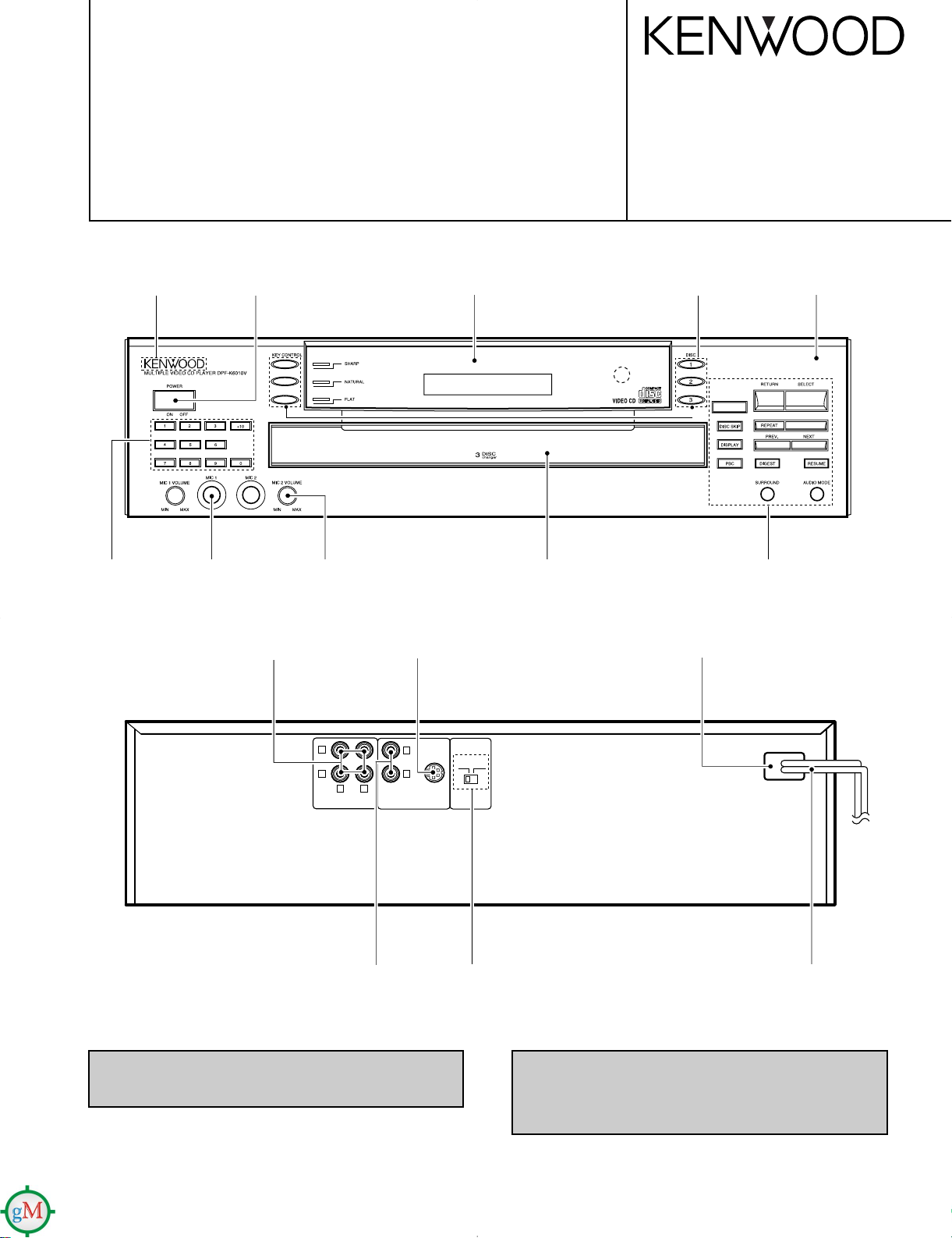
DPF-K6010V
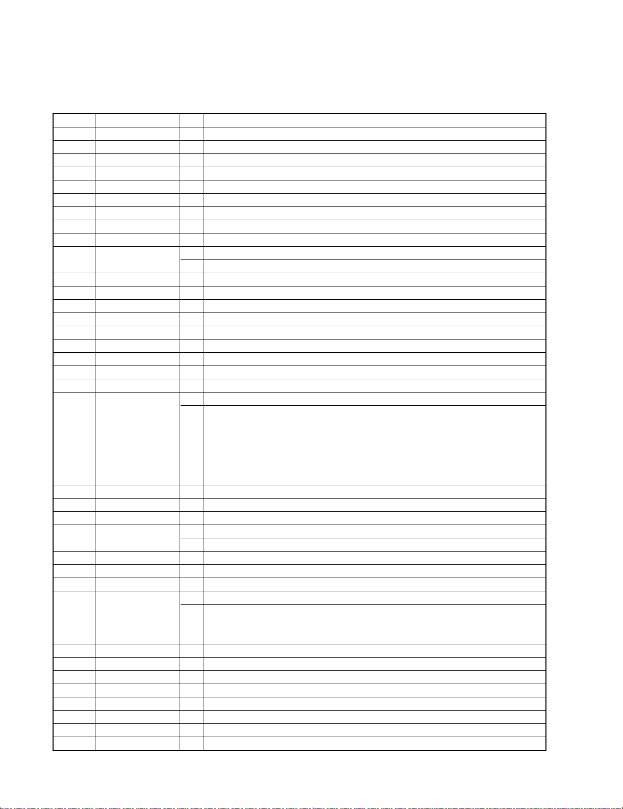
No. Name I/O Description
1 VDD – Voltage supply for 3.3V.
2 RAS O DRAM row address strobe (active low).
3 DWE O DRAM write enable (active low).
4~12 MA0~MA8 O DRAM multiplexed row and column address bus.
13~28 DBUS0~DBUS15 I/O DRAM data bus.
29 RESET I System reset (active low).
30 VSS – Ground.
31 VDD – Voltage supply for 3.3V.
32~39 YUV0~YUV7 O Y is luminance, UV are chrominance data bus for screen
Video interface. YUV (0~7) for 8 bit YUV mode.
40 VSYNC I/O Vertical sync for screen video interface, programmable for rising or falling edge.
41 HSYNC I/O Horizontal sync for screen video interface, programmable for rising or falling edge.
42 CPUCLK I RISC and system clock input.
CPUCLK is used only if SEL PLL [1 : 0] = 00.
43 PCLK2X I/O Pixel clock ; two times the actual pixel clock for screen video interface.
44 PCLK I/O Pixel clock qualifier in for screen video interface.
45 (GFS) AUX0 I/O GFS input from IC2 (CXD2500BQ).
46 (SQSO) AUX1 I/O Inputs 80 bit Sub Q and 16 bit PCM peak-level data.
47 (VFD D) AUX2 I/O Auxiliary control pins.
48 (MUTE) AUX3 I/O "H" for muting, "L" for release.
49 (IRQ) AUX4 I/O Auxiliary control pins.
50 VSS – Ground.
51 VDD – Voltage supply for 3.3V.
52 VFD L I/O Auxiliary control pins.
53 STB I/O Auxiliary control pins.
54 VFD CK I/O Auxiliary control pins.
55~62 LD0~LD7 I/O RISC interface data bus.
63 LWR O RISC interface write enable (active low).
64 LOE O RISC interface output enable (active low).
65~67 LCS (3, 1, 0) O RISC interface chip select (active low).
68~79 LA0~LA11 O RISC interface address bus.
80 VSS – Ground.
81 VPP – Digital supply voltage for 5V.
82~87 LA12~LA17 O RISC interface address bus.
88 ACLK I/O Master clock for external audio DAC (8.192MHz, 11.2896MHz, 12.288MHz, 16.9344
MHz, and 18.432MHz).
O Dual-purpose pin. AOUT is the audio interface serial data output
Pins SEL PLL [1 : 0] select phase-lock loop (PLL) clock frequency CPUCLK for the
ES3210 : 00 = bypass PLL.
89 AOUT/SEL PLL0 I 01 = 54MHz PLL.
10 = 67.5MHz PLL.
11 = 81MHz PLL.
90 ATCLK I/O Audio transmit bit clock.
O Dual-purpose pin. ATFS is the audio interface transmit frame sync.
91 ATFS/SEL PLL1 IPins SEL PLL [1 : 0] select phase-lock loop (PLL) clock frequency CPUCLK for the
ES3210. See the SEL PLL0 pin above for the settings.
92 DOE O DRAM output enable (active low).
93 AIN I Audio interface serial data input.
94 ARCLK I Audio receive bit clock.
95 ARFS I Audio interface receive frame sync.
96 TD MCLK I TDM interface serial clock.
97 TD MDR I TDM interface serial data receive.
98 TD MFS I TDM interface frame sync.
99 CAS O DRAM column address strobe bank 0 (active low).
100 VSS – Ground. 5
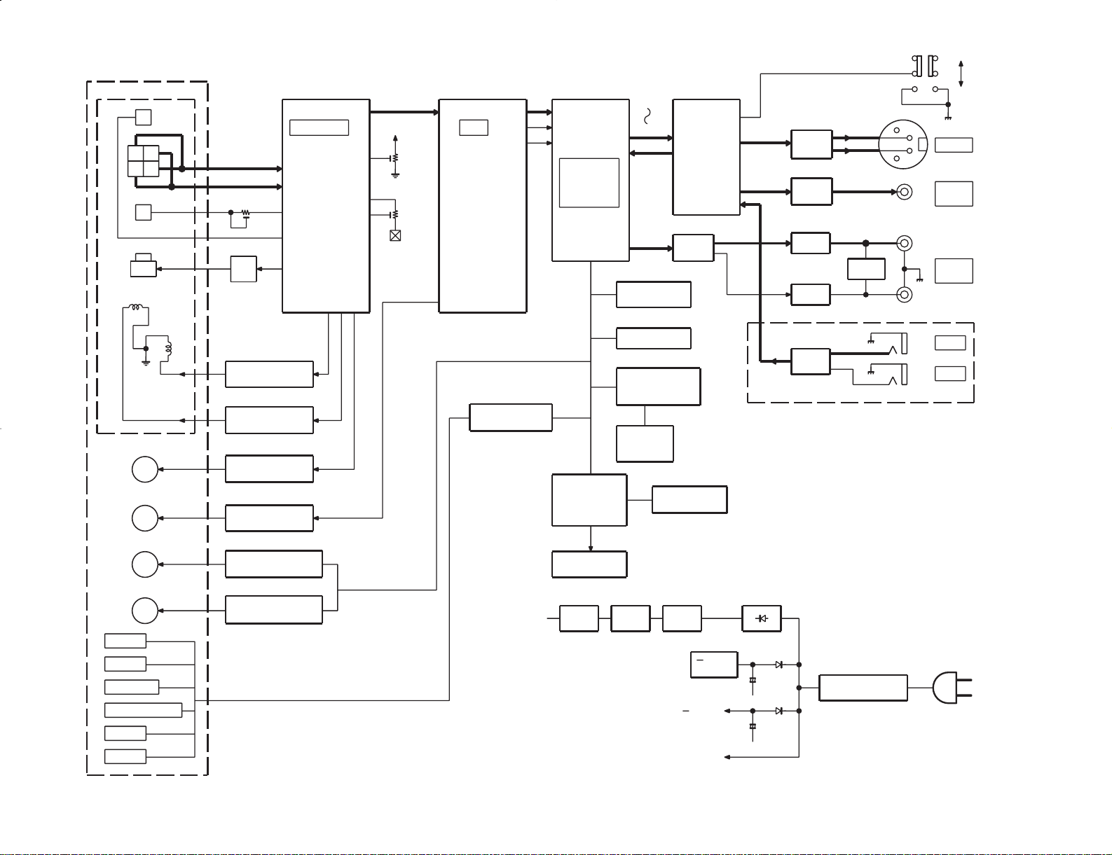
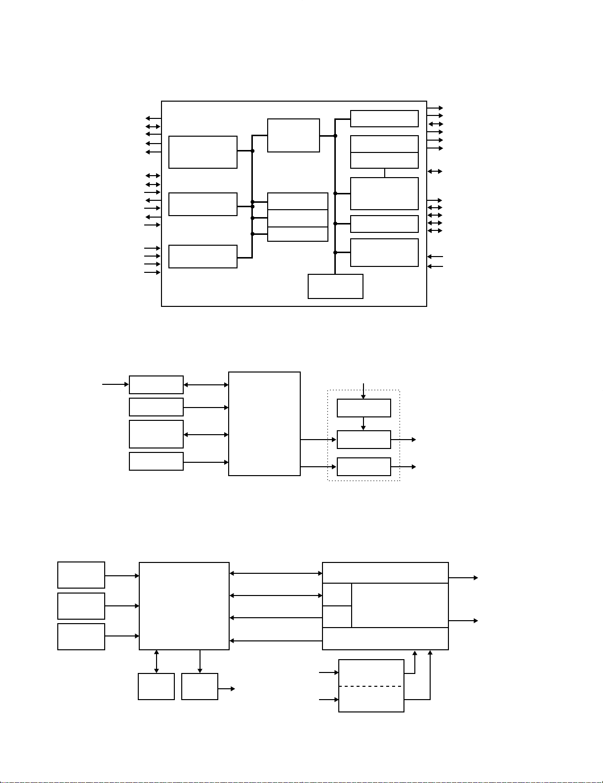
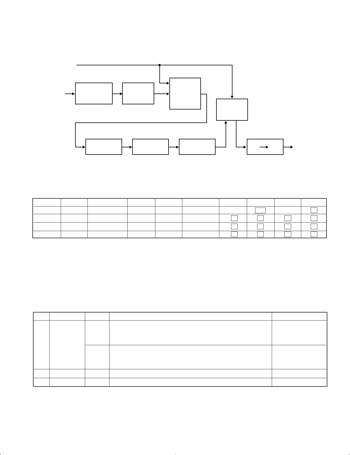
CIRCUIT DESCRIPTION
1. MPEG Microprocessor : IC11 (E3210F)
Pin description
DPF-K6010V(K)COVER1,1(98.12.1010:54 y[W 10