manuals.online logo
Brands
  1. Home
  2. •
  3. Brands
  4. •
  5. Kenwood
  6. •
  7. Transceiver
  8. •
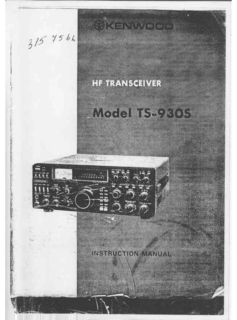
  9. Kenwood TR-7730 User manual

Kenwood TR-7730 User manual

Other manuals for TR-7730

2

Other Kenwood Transceiver manuals

Kenwood TM-701E User manual

Kenwood

Kenwood TM-701E User manual

Kenwood TS-870S User manual

Kenwood

Kenwood TS-870S User manual

Kenwood Nexedge NX-320E User manual

Kenwood

Kenwood Nexedge NX-320E User manual

Kenwood TS-950 series User manual

Kenwood

Kenwood TS-950 series User manual

Kenwood TS-511S User manual

Kenwood

Kenwood TS-511S User manual

Kenwood TK-2107 User manual

Kenwood

Kenwood TK-2107 User manual

Kenwood TS-890S User manual

Kenwood

Kenwood TS-890S User manual

Kenwood NEXEDGE NX-220 User manual

Kenwood

Kenwood NEXEDGE NX-220 User manual

Kenwood TH-215A User manual

Kenwood

Kenwood TH-215A User manual

Kenwood TS-450S User manual

Kenwood

Kenwood TS-450S User manual

Kenwood TK-860HG User manual

Kenwood

Kenwood TK-860HG User manual

Kenwood TK-261 User manual

Kenwood

Kenwood TK-261 User manual

Kenwood TS-990S Manual

Kenwood

Kenwood TS-990S Manual

Kenwood TM-401A User manual

Kenwood

Kenwood TM-401A User manual

Kenwood TM-321A User manual

Kenwood

Kenwood TM-321A User manual

Kenwood Trio TS-520 User manual

Kenwood

Kenwood Trio TS-520 User manual

Kenwood TS-890S Operating manual

Kenwood

Kenwood TS-890S Operating manual

Kenwood NX-320 Series User manual

Kenwood

Kenwood NX-320 Series User manual

Kenwood TK-2140 User manual

Kenwood

Kenwood TK-2140 User manual

Kenwood TK-385 User manual

Kenwood

Kenwood TK-385 User manual

Kenwood TH-27 Series User manual

Kenwood

Kenwood TH-27 Series User manual

Kenwood TK-2402 User manual

Kenwood

Kenwood TK-2402 User manual

Kenwood TS-950SDX User manual

Kenwood

Kenwood TS-950SDX User manual

Kenwood TS-870S User manual

Kenwood

Kenwood TS-870S User manual

Popular Transceiver manuals by other brands

City Theatrical SHoW DMX SHoW Baby user manual

City Theatrical

City Theatrical SHoW DMX SHoW Baby user manual

Standart Horizont HX407 owner's manual

Standart Horizont

Standart Horizont HX407 owner's manual

B&G V90S quick start guide

B&G

B&G V90S quick start guide

VictelGlobal ALK300 series Operation manual

VictelGlobal

VictelGlobal ALK300 series Operation manual

Cactus Wireless Flash Transceiver V6 user manual

Cactus

Cactus Wireless Flash Transceiver V6 user manual

Yaesu FT-11R user guide

Yaesu

Yaesu FT-11R user guide

Skanti TRP 5000 instruction manual

Skanti

Skanti TRP 5000 instruction manual

ELECRAFT KX3 Installation and operation guide

ELECRAFT

ELECRAFT KX3 Installation and operation guide

American Lighting DMX512 quick start guide

American Lighting

American Lighting DMX512 quick start guide

Furuno FM-77 Operator's handbook

Furuno

Furuno FM-77 Operator's handbook

Yaesu FT-7B manual

Yaesu

Yaesu FT-7B manual

Mizuho MX-2 Operating & assembly instruction

Mizuho

Mizuho MX-2 Operating & assembly instruction

Blitz MJ-398U instruction manual

Blitz

Blitz MJ-398U instruction manual

Utilicom LongRanger 2050 Operator's manual

Utilicom

Utilicom LongRanger 2050 Operator's manual

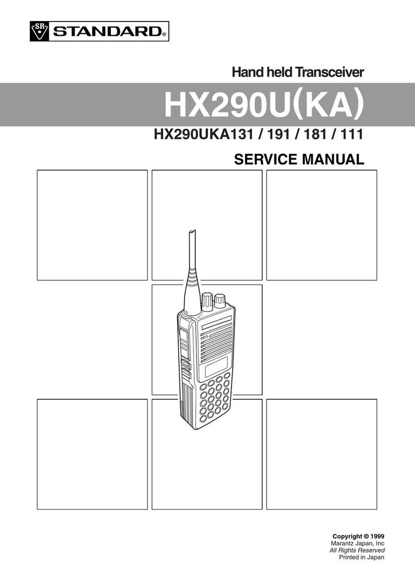
Standart HX290UKA Service manual

Standart

Standart HX290UKA Service manual

Altronix Pace1PTM installation guide

Altronix

Altronix Pace1PTM installation guide

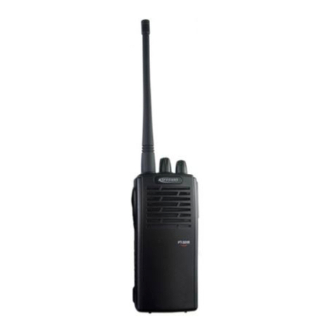
Kirisun PT2208 instruction manual

Kirisun

Kirisun PT2208 instruction manual

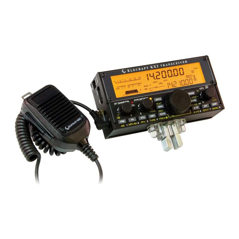
ELECRAFT KX2 manual

ELECRAFT

ELECRAFT KX2 manual

manuals.online logo
manuals.online logoBrands
  • About & Mission
  • Contact us
  • Privacy Policy
  • Terms and Conditions

Copyright 2025 Manuals.Online. All Rights Reserved.

YKENWOOD
SERVICE
MANUAL
R-7730
VHF
FM
TRANSCEIVER
®KENWOOD
2m
FM
TRANSCEIVER
BUBY
1
2
POWERS
VOL
SQUELCH
a
2
yo
-
o
Oty.
al
.
A
TR-7730
ON
AiR
RPT
56
CONTENTS
SPECIFICATIONS
........
0.2...
00
eee
eee
2
DISPLAY
UNIT
(X54-1520-11)
2.2...
ee
ee
12
CIRCUIT
DESCRIPTION
.................00.
2
M,
MR
BOARD
(J25-2757-14)
2.0...
ee
ee
12
PC
BOARDS
M.S,
TONE
BOARD
(J25-2757-14)
..
0.0.00.
06.
12
RX.TX
UNIT
(X44-
1450-10)
(K,
M
TYPE).
......
8
SCAN,
HOLD
BOARD
(J25-2758-14)
.........
12
RX.TX
UNIT
(X44-1450-51,
-61)
(T,
WTYPE)....
9
PARTS
LIST
2...
ee
eee
13
FINAL
UNIT
(X45-1190-10)
2.2...
eee
eee
10
DISASSEMBLY
...
0.0.0.0...
0.0.0
eee
18
PLL
UNIT
(X50-1750-10)
2.2.2.2
eee.
10
LEVEL
DIAGRAM.........
00.20.2202
eee
20
CONTROL
UNIT
(X53-1230-10,
-61)
.........
11
ADJUSTMENTS
©.
2...
0...
cee
ee
nee
21
M.CH
BOARD
(J25-2715-04)
..
0.2...
2.
eee
11
PACKING
©...
6.
ee
eee
28
RPT
BOARD
(J25-2744-04)
1...
.........0..
11
SCHEMATIC
DIAGRAM
(K,
MTYPE)........
...
29
SCHMITT
BOARD
(J25-2755-14)
............
11
SCHEMATIC
DIAGRAM
(T,
WTYPE)...........
30
10K/5K
or
25K/5K
(J25-2756-04)
...........
11
REFERENCE
DATA
.........
cee
ee
ee
31
H|/LOW
BOARD
(J25-2756-04)
........0....,
11
BLOCK
DIAGRAM
...............
BACK
COVER
TR-7730
SPECIFICATIONS/CIRCUIT
DESCRIPTION
[General]
SeMICONdUCtOIS
.........cccee
eee
cec
seen
eeeeteteeeneneees
ICs
15
(K,M)
16
(W,
T)
Transistors
46
(K,M)
49
(W,
T)
FETs
7
Diodes
91
(K,M)
95
(W,
T)
Frequency
range
..........-.2-eeeeeeeceeeseeeenaeee
vanes
144.000
to
147.995
MHz
(K,M)
144.000
to
145.995
MHz
(W,
T)
Frequency
synthesizer
’
Digital
contro!,
phase
locked
VCO
Mode
.......c.ccccccecsccerssnececeeseneeceneeeentetseneeeee
FM
(F3)
Antenna
impedance
..................ccsceeeseeeeeeneee
50
ohms
Power
requireMent
..........cccceceeeeetee
seen
eeeeeen
eee
13.8
VDC
415%
Grounding
...........ceeeeceeeceenee
et
ee
ener
eeeenen
tae
nene
Negative
Operating
temperature
Current
Crain
.........cc
ce
cececsece
ec
eereeeeteteeeaeer
erent
—20°C
to
+60°C
0.4A
in
receive
mode
with
no
input
signal
5.5A
in
HI
transmit
mode
(Approx.)
3A
in
LOW
transmit
mode
(Approx.)
Less than
2.5
mA
for
memory
back
up
(from
power
supply)
Dimensions.
...........c..ccceeeeeecteeeeeseentereeeenenans
147.5
mm
(5-3/4)
wide
51.5
mm
(2”)
high
198.0
mm
(7-3/4")
deep
(projections
excluded)
Weight........-:::.ccsseeeeecceeecneeseeseessseaeeeeseneeees
1.5
kg
(3.3
Ibs)
(Approx.)
{Transmitter
Section]
RF
output
power
(at
13.8
VDC,
50
OD
load)
........0..
cece
HI
25
Watts
min.
LOW
5
Watts
approx.
(Adjustable)
Modulation
............:.0:0600
Frequency
tolerance
(-—10°C~
+50°C)
Variable
reactance
direct
shift
Less than
+
20x
10°
Spurious
radiation
.........cccccccceeeeeeeeeeeeneneeeeeee
HI
Less
than
—
60
dB
LOW
Less
than
—
53
dB
Maximum
frequency
deviation
(FM}
...............
+5
kHz
Microphone
.............cccceccen
eer
en
eee
eeeene
ene
eneenees
Dynamic
microphone
with
PTT,
up,
down,
switches,
500
2
{Receiver
Section]
CirCUitry
0.0...
ccccceeee
eee
enecneneneneeereeteenteneeetner
Double
conversion
superheterodyne
Intermediate
frequency
..........:ccccceeveeeeeeenerees
1st
IF
10.7
MHz
2nd
IF
455
kHz
Receiver
Sensitivity
.........cccccecnsesseeveeeueeneeeers
Better
than
0.5
»V
for
30
dB
S/N
Better
than
0.25
zV
for
12 dB
SINAD
Receiver
selectivity
...........ccccceeeesenseeeeeeneeeees
More
than
12
kHz
(—6
dB)
Less
than
25
kHz
(—
60
dB)
Spurious
reSPONSe............
ccc
ceeeecetee
eee
er
eee
ees
Better
than
60
dB
Squelch
sensitivity
...
eesvsasssesesesteaeesestenes
0.16
pV
(threshold)
Audio
OUtPUL
2...
cee
ece
ete
c
cer
eeeenea
rea
neaennees
More
than
2.0
watts
across
8
ohm
load
(10%
dist.)
Note:
Circuit
and
ratings
are
subject
to
change
without
notice
due
to
developments
in
technology.
NOTE
:
Letter
designations
used
in
this
manual
:
K
ULS.A.
X
AUSTRALIA
T
BRITAIN
M
GENERAL
MARKET
W
EUROPE
<
RECEIVER
SECTION
>
RX.TX
UNIT
(X44-1450-
XX)
The
antenna
signal
is
applied
to
the
RF
amplifier
(Q3
:
3SK76},a
dual
gate
MOS
FET
and
helical
resonator
L5
(3
poles)
and
L6
(2
poles),
and
is
then
converted
to
the
10.7
MHz
Ist
IF
signal
by
O04,
the
1st
mixer.
A
2-stage
MCF
(Monolithic
crystal
filter)
is
used
in
the
1st
IF
stage.
All
this
achieves
high
dynamic
rane
and
high
sensitivity.
The
1st
IF
signal,
after
passing
through
the
MCF,
is
mixed
with
the
10.245
MHz
2nd
local
oscillator
signa,
generated
by
05
to
obtain
a
455
kHz
2nd
IF
signal.
This
signal
passes
through
the
ceramic
filter
ICF7>W455F)
and
is
amplified
by
[C1,
Q7
through
Q10,
andis
then
de-
modulated.
An
S
meter
signal
is
obtained
by
ditecting
the
signal
from
the
collector
of
Q7
by
diodes
D2
ad
D3,
and
is
then
applied
to
the
display
unit.
The
S
meter
uses
8
LEDs,
and
indicates
6
amber
and
1
red
LE)
when
the
antenna
input
level
is
15
dBu.
TR775!
CIRCUIT
DESCRIPTION
Item
Rating
Nominal
center
frequency
(fo)|10.7
MHz
Pass
bandwidth
fo+7.5kHz
or
more
at
3dB
fo
+25 kHz
or
less
at
40
dB
fo
+45
kHz
or
fess
at
60
dB
Attenuation
bandwidth
70
dB
or
more
within
fo
+1
MHz
80
dB
or
more
within
fo—
(910
kHz
+
10
kHz)
Guaranteed
attenuation
40
dB
or
more
within
fo
to
Spurious
fo
+500
kHz
Ripple
1,0
dB
or
less
Loss
1.5
dB
or
less
Input
and
Output
impedance
|3kQ
Operating
temperature
—20°C~+70°C
Table
1
MCF
(L71-0219-05)
(RX.TX
unit,
L17)
Item
Rating
Nominal
center
frequency
455
kHz
6
d8
bandwidth
+6
kHz
or
more
50
dB
bandwidth
+12.5
kHz
or
less
Ripple
(within
455
+4
kHz)
3
dB
or
jess
Loss
6
dB
or
less
Guaranteed
attenuation
(within
455+
100
kHz)
35
dB
or
more
Input
and
output
impedance
2.0
k®
Table
2
Ceramic
filter
CFW455F
(L72-0315-05)
(RX.TX
unit,
L18)}
The
VCO
signal
is
amplilfied
by
Q2
and
Q3
in
the
PLL
unit,
and
then
applied
to
the
RX.TX
unit
via
the
LT
terminal.
The
signal
is
amplified
by
Q1
and
Q2
before
it
is
applied
to
the
power
module.
This
simple
transmitter
structure
pro-
vides
superior
spurious
radiation
characteristic.
The
HIGH/LOW
switch
signal
is
applied
to
Q28,
Q22
and
Q21
in
the
RX.TX
unit,
which
controls
the
B+
voltage
applied
to
the
driver
stage
(O2),
so
that
final
input
and
out-
put
power
is
varied.
The
RF
meter
is
adjusted
so
that
6
amber
LEDs
light
at
HIGH
power.
However,
the
number
of
LEDs
on
may
vary
according
to
the
VSWR
of
the
antenna
system.
Terminal
:
RE
Input
:
Vee
1
:
GND
:
Vec
2
:
RF
Output
abON=—
Fig.
1
POWER
MODULE
VP-15E
1305
Item
Rating
Center
frequency
and
deviation
455
kHz
+1.0
kHz
Peak
separation
15
kHz
or
more
Voltage
sensitivity
(at
455
kHz)|
15
mV/kHz
or
more
Item
Symbol!
|
MAX
Rating
|
Condition
Power
supply
voltage
Vec
17V Te=
25°C
DC
current
lec
BA
Tc
=
25°C
Operating
case
temperature
Top
—30~
100°C
Storage
temperature
Tsta
|
—40~110°C
—10°C~+50°C
Operating
temperature
Table
3
Ceramic
discri
CF
Y455S
(L79-0446-05)
(RX.TX
unit, L179)
<
TRANSMITTER
>
RX.TX
UNIT
(X44-1450-
XX)
The
microphone
signal
is
amplified
and
limited
by
IC2
(TA7061AP),
and
is
then
applied
to
D1
(1S2208)
in
the
PLL
unit
to
directly
modulate
the
VCO.
The
VCO
gener-
ates
144~
145.995
MHz
(W,
T)
or
143.9~
148.995
MHz
(K,
M)
according
to
the
control
signa!
from
the
microprocessor.
VP-15E1305
MAX
Rating
It
Symbol]
Conditi
Rating
Unit
em
ymbo
‘ondition
MIN
|
TYP
|
MaAx
|
UNI
f
range
f
144
148
|
MHz
Power
input
Pin
250
mw
Pin
=
250
mw
Power
output
Po
Vee
=
13.0V
30
Ww
Operating
voltage
Vec
13.0
Vv
Input
and
out-
Pin
=
250
mw
put
impedance
Zz
Vec
=
13.0V
50
2
a
Pin
=
250
mW
Total
efficiency|
nT
Vee
=
13.0V
45
50
;
%
VP-15E1305
Electrical
Characteristic
TR-7730
CIRCUIT
DESCRIPTION
PLL
CIRCUIT
(X50-
1750-10)
VCO
Q1
:
2SK19
(GR)
generates
143.900~
148.995
MHz
(K,
M)
or
144.00~
145.995
MHz
(W,
T)
during
transmission
and
133.200~
138.295
MHz
(K,
M)
or
133.30~135.295
MHz
(W,
T)
during
reception.
The
VCO
signal
is
buffered
by
Q2
and
amplified
by
O3
and
Q4.
It
is
then
mixed
with
the
HET
signal
(from
Q5)
by
Q12
to
obtain
a
PLL
IF
signal
(5.4~
10.495
MHz
[K,
M}
or
5.5~
7.49
MHz
[W,T]).
The
HET
signal
is
generated
by
O5,
a
third
overtone
oscilla-
tor
using
a
46.1666
MHz
crystal
to
generate
138.5
MHz
for
transmission
and
a
42.6
MHz
crystal
to
generate
127.8
MHz
for
reception.
Both
frequencies
are
shifted
5
kHz
when
the
5K
control
signal
from
the
control
unit
(X53-1120-10)
is
applied
to
D9
and
D10
to
shunt
TC3
and
TC4.
The
resonant
frequencies
of
L5,
L7,
L10,
and
the
VCO
tank
circuit
and
the
HET
frequency
are
switched
for
recep-
tion
and
transmission
using
the
8R
(8V
DC
during
recep-
tion)
and
8T
(8V
DC
during
transmission)
control
lines.
The
PLL
IF
signal
is
amplified
by
010
and
buffered
by
011
and
Q9,
and
then
applied
to
pin
2
of
IC3
(TC9122P)
the
programmable
divider.
1C3
is
supplied
with
frequency
divid-
ing
data
from
the
control
unit
:550~
1049
(K,
M}
or
550~
749
(W,
T)
in
BCD,
and
the
PLL
IF
frequency
is
also
divid-
ed
to
a
10
kHz
signal
for
a
phase-lock
comparison
signal.
IC2
(TC5082P-GL)
is
the
10.24
MHz
oscillator.
Its
output
is
divided
by
1024
to
10kHz
for
IC1‘s
reference
signal.
These
comparison
and
reference
signals
are
input
to
the
phase
comparator
(IC1
:
TC5081P)
and
the
resultant
DC
output
signal
is
applied
through
the
low
pass
filter
Q8
and
Q7
to
the
VCO
tank
circuit
through
varicap
diode
(D2
:
1$2208)
to
control
the
VCO
output
frequency.
if
the
PLL
unlocks,
the
voltage
at
IC1
pin4
drops
to
turn
off
Q6
and
D11,
which
shuts
off
Q3.
[
sw
AMP
MOD
TX,RX
UNIT
01
——~al
FROM
Ic2
182208
F.CONT
D2
182208
N
=
550~749
(Ww,
T)
N
=
540~1049
(K,
M)
CONTROL
UNIT
FROM
1C1
TX
:
143.900~148.995
MHz
(K,
M)
RX
:
133.200~138.295
MHz
(K,
M)
TX
:
144.00~145.98
MHz
(W,
T)
RX
:
133.30~134.30
MHz
(W,
T)
TX
:
138.5MHz
RX
:
127.8MHz
|
5.5
MHz~7.49
MHz
(W,
T)
5.4
MH2~10.49
MHz
(K,
M)
TC3,
4
7
TX
:
46.1663MHz
(X2)
RX:
42.6Miz
(X1)
aQ1li~g
28C460
(B)
CONTROL
UNIT
+5kHz
SHIFT
10.24MHz
OSC/DIVIDE
(1/1024)
mm
on
Fig.
2
PLL
unit
block
diagram
GNO
Pout
De
Dt
Ca
C3
C2
Ci
B4
;
Symbol
N
Ce
it
emarks
[ia]
fi7]
[ie] [ts]
14
fa]
fiz]
|
[to]
ymbo!
ame
lontent
and
operation
|
Pin
Programmable
counter
Programmable
counter
input
terminal
to
which
the
signal
to
be
Bulld-in
bias
h
‘
input
terminal
divided
rs
input
crreuit
GND
OUT
Pout
Programmable
counter
Programmabie
counter
output
terminal.
Outputs
1/N
of
the
D
output
terminal.
imput
frequency.
The
output
pulse
width
equals
5
bit
of
-
2
the
input
n
c
4
J
Ai~Aa
|
x1
Terminal
to
set
the
dividing
ratio.
The
followmg
input
Built-in
BR
~<
B8,~8&
|
x
10
Program
input
|
combination
is
prohibited
pull-down
4
Ci~C.
|
x
100
terminals
AL
Ar
Ay
Ae
8
Br
By
Be
Cy
Cr
Cs
Co
Di Di
cesistor
A
“
0,~O.
}
=
1000
10000
000
060
000
0 0
4
6
10000000
0
00
0
0
Voo_IN
1
1000
0000000
0
0
4
0
0
100000000
0
0
2,
4
1°01
00
000
000
0
0
0
ce)
1 1
o
0
0
0600
0
0 6 0
0
Qo
EE
a
Voo
Pin
At
A2
AB
Aa
Bt
B22
B3
4
Fig.
3
TC9122P
(PLL
unit,
1C3)
Table
4
TC9122P
(PLL
unit,
IC3)
TR-773(
CIRCUIT
DESCRIPTION
XT
xT
XTOUT
CONTROL
CIRCUIT
(X53-
1230-10)
Fig.
6
shows
a
block
diagram
of
the
control
circuit,
which
uses
a
microprocessor
to
minimize
the
number
of
per-
ipheral
circuits.
@
Frequency
Indicator
The
frequency
indicator
uses
a
4
digit
dynamically
driven
LED
display.
The
BCD
data
from
the
microprocessor
D
port
(pins
8~11)
is
converted
by
decoder
driver
1C2
(TC
5022BP}
into
the
segment
signals
which
are
applied
to
the
corresponding
segments
of
all
digits.
The
signals
from
the
E
port
(pins
12~15)
turn
ON
Q7
through
Q10
(2SC1959)
to
light
the
digits.
VOD
GND
ow
46
atisi0
08
@
PLL
Data
(Frequency
Dividing
Data}
The
frequency
dividing
data
is
output
from
ports
D,
E,
G,H
PIN
NO
8
7
6
4
1
and
|
(pins
9~11,
12,
and
22~32)
in
BCD.
It
is
550
when
PIN
NAME
Q,
Qh
On
Qu
|
XTout
“VF
is
displayed,
650
when
5.7/7
is
displayed,
749
when
—_
Dividing
ratio
|
1/256
|1/1024|
1/2048]
1/4096
|
1/1
5.44
is
displayed
and
1049
(K,
Monly)
when
2.4%
is
displayed.
seatbut
frequency]
40
kHz
|10
kHz|
5
kHz
|2.5
kHz
|
10.24
©
Reset
Circuit
;
Current
flows
through
D36
when
the
power
source
voltage
Fig.
4
TC5082P-GL
(PLL
unit,
1C2)
supplied
to
the
microprocessor
exceeds
about
3.5V.
The
collector
voltage
of
O5
(2SC1815
(Y)})
then
becomes
H
and
a
pulse
is
generated
by
the
CR
differentiating
circuit.
This
|
|
| f
|
FL.
pulse
is
applied
to
and
resets
the
microprocessor.
SIN
@
Switch
Circuit
Rin
|
|
|
|
| |
[
|
One
terminal
of
each
contro!
switch
is
connected
to
one
of
the
control
pulse
signal
output
terminals
of
the
micropro-
Poor
—
HIGH
IMPEDANCE
JL
_--
JL
—_---
cessor
and
the
other
terminal
to
one
of
the
input
terminals.
Ly
When
a
control
switch
is
turned
ON,
the
corresponding
PHASE
OUT
Ise
signal
is
input
to
the
corresponding
input
ter-
TP
LI
LJ
output
pulse
sig
p
p
g
inp
minal
and
the
prescribed
function
is
performed
Diodes
are
used
to
prevent
the
control
pulse
signals
from
being
input
to
the
wrong
circuit.
@
Encoder
and
UP/DOWN
Switch
Input
Circuit
The
mechanical
encoder
output
signals
are
appl
ied
to
the
Schmitt
circuits
formed
by
I1C102
(TC7404UBP},
then
R
@-tdo
BD:
applied
to
part
A
(pins
33~36)
of
the
microprocessor.
The
microprocessor
judges
UP/DOWN
and
counts
the
number
POour
of
applied
pulses.
One
turn
of
the
dial
equals
50
step
P
output.
—{
>»
®
Scan
Circuit
f
Scan
operation
is
controlled
entirely
by
the
micio
processor
.
—@
voo
It
starts
when
the
SCAN
switch
is
pressed
andstops
when
either
the
HOLD
switch
is
pressed
or
the
transmit
signal
imc
vss
(8T)
becomes
H.
Scan
operation
temporarily
st
ops
when
;
the
squelch
stop
signal
(input
to
the
SS
termiml
)
becomes
Fig.
5-A
TC5081P
(PLL
unit,
1C1)
Timing
chart
Voo
,
H.
Variation
of
the
frequency
dividing
data
for
the
least
PHASE
.
oe
woe,
oe
. .
oo
OUT
significant
digit
is
detected
by
the
circuit
crtsisting
of
Q1,
Q2
and
the
OR
circuit
D10~13
so
tha
a
pulse
is
Ain
@—f>o—
Aout
obtained
every
time
the
data
changes.
This
pulse
signal
is
; . ;
.
applied
to
the
scan
stop
terminal
(pin
4)
of
the
Micropro-
Fig.
5-B
TC5081P
(PLL
unit,
1C1)
Equivalent
circuit
cessor
to
momentarily
suspend
slow
scannity
after
the
frequency
has
been
changed.
TR-7730
CIRCUIT
DESCRIPTION
LED
7
Decoder
~
9997007
river
ie
ie
ic2
E3%E2461
4E0
15
414
113
[12
Latch
ICc3
4
89,10,11
EO
4
——
EO
5kHz
data
=
“
°
(
GE
10
kHz
data
ForPLL
MHz
data
Abit
2bit
PLL
|
H
=
>
100
KH?
data
q
19
leh
19-40
“pr
ch
19—
V
Memory
2en
19-39
{C1
——_&—=—_——
MHz
data
.
channe
3ch
19-38
Sbit
@
M
switch
14438
switch
ach
19-+37
INT
@
MR
switch
14-37
Sch
19-+37.38
+)
@
SCAN
Ni
Vec
~~
switch
1337
on
RES
@
HOLD
7
c
A
mu
Reset
by
switch
1340
@
MS
switch
13-38
4
2
2
+f
33,34 35,36
.
UP/DOWN
Schmitt
switch
(MIC)
Power
supply
|
4°
Transmit
signal
(8T)
for
backup
Squelch
stop
signal
(SS)
Rotary
a
Other
circuit
encoder
Power
supply
IC4
Fig.
6
Control
unit
block
diagram
POWER
SW
Pin]
Pin
|
input
[Output
Note
Pulse
Pin|
Pin
|
Input
|
Output
Note
Pulse
No.
signal
|
signal
signal
No,
signal
|
signal signal
1
CL1
Clock
signal
400
kHz
(Level
at
14500
MHz)
2
{Poo
Normally
L
23
[pot
©
|b
|toKte
deta
signals
I
z
data
signals
3
|Pci_
|
0
Normally
L
24
|PG2
o
|e
[for
PLL
me
4
|PC2
i)
Squelch
signal,
SCAN
stops
25
|PG3
o
|p
iL
when
H.
26
|PHO
OIA
rH
5
PC3
ie)
Normally
L,
H
during
transmis-
27
~|PH1
o
|p
|
100
kHz
data
!
L
sion.
28
|PH2
o.
Ic
{signals
for
PLL
4
6
INT
[e)
Normally
H
29
IPH3
Oo
|D
ia
7
RES
°
Microprocessor
is
reset
when
H.
30
|PIO
O
JA
)1MHzdata
im
8
PDO
re)
fo)
oO
31
=
jPIi
oO
|B
|
sont
for
|
H
9
|PD1
ro)
re)
10
kHz,
100
kHz,
and
MHz
ro)
32
|PI2
oO
{C
/PLL
iH
10
|PD2
[e)
Oo
digit
signals
are
output.
ie)
33
|PAO
[e)
Encoder
signal
11
[PDs
°
©
°
34
|PAI
[@)
Encoder
signal
12
|PEO
OQ
|5kHz
digit
signal
is
output.
ie)
35
|PA2
Oo
Normally
4,
L
when
MIC
UP
13
|PE1
O
{10
kHz
digit
signal,
SCAN,
o)
switch
is
pressed.
HOLD
or
M.S
is
output.
36
|PA3
O
Normally
H,
L
when
MIC
14
|PE2
O
{100
kHz
digit
signal,
Mor
MR
ie)
DOWN
switch
is
pressed.
is
output.
37
|PBO
fo)
MR,
SCAN,
Memory
CH4
or}
ce)
15
|PE3
O11
MHz
digit
signal
is
output.
re)
pulse
signal
is
input.
16
|PFO
Not
connected.
38
|PB1
e)
M,
MS,
Memory
CH3
or
5
pute
ie)
17,
(PFI
O
|
\1MHzdata
signals
|
L
signal
is
input.
18
IPF2
fe)
for
PLL
UL
39
|PB2
(e)
Memory
CH2
pulse
signal
is
1°)
19
|PF3
©
jMemory
output
signal
fo)
-
input.
5
20
[TEST
Normally
H
40
|PB3
|
0
sional
aia
CH1
pulse
21
Ice
5V
power
supply
a1
GND
GND
-
42
|CLO
Clock
signal
400
kHz
Table
5
Microprocessor
Functions
.PD650C-021
(Control
unit,
1C1)
TR7dl
CIRCUIT
DESCRIPTION
@
Power
Supply
for
control
system
Transistor
O6
(2SC496
(Y))
generates
5V
for
the
frequency
display.
A
6V
AVR
(Automatic
voltage
regulator)
IC
(1C4
:
NJM78LO6K)
supplies
power
to
the
microprocessor
through
diode
D18.
@
Backup
Circuit
The
level
at
the
microprocessor
INT
terminal
becomes
L
when
the
POWER
SW
is
turned
OFF,
and
the
micropro-
cessor
enters
the
backup
mode.
In
this
mode,
all
output
ports
are
low
to
minimize
power
consumption.
At
power
OFF,
the
backup
supply
is
024
(2SC2603
(E))
on
the
RX.TX
unit.
When
the
POWER
SW
is
turned
ON,
the
levels
at
both
the
INT
(pin
6)
and
UP/DOWN
(pins
35
and
36)
terminals
be-
come
H,
returning
the
microprocessor
to
operation
as
be-
fore
the
POWER
SW
was
turned
OFF.
Input
port
B
pins
(87~40)
are
grounded
by
Q3
and
O4
when
the
POWER
SW
is
turned
OFF,
and
scan
operation
is
stopped
by
momentarily
simulating
the
transmission
mode
through
Q11.
Upper
=
Pin
No.
24
13
ean
|
FM
81
@>
AM
“p
a
RBI
(2
1)
RBO
TTT
PM
Alarm
ORIVER
|
ORIVER
|
Lic
=
~
+}
borers
i
5)
0
|
*—
Voo
:
Pin
No.
1
dol
TCower
do2
1
@
L
@e
|
)
(aes
[Colon
\sea
°®
aco
TO
ac
|
L
l
7-
SEGMENT
NB)
4
!
oer
|
Cc
é
{pe
'
:
©
necooes
io.
|
|
PIN
NO
FUNCTION
PIN
NO
FUNCTION
0
®
9)
9
|
l
1
PM
Anode
13
FM,
Alarm
Cathode
L-—4
Lo
=
2
Dig
1
Cathode
14
FM
Anode
. .
.
.
.
3
Seg
d
Anode
15
Sega
Anode
Fig.
7
TC5022BP
(Control
unit,
1C2)
Equivalent
circuit
4
dp
1
Anode
16
dp
2
Cathode
5
Dig
2
Cathode
17
Upper/Lowe
Colon
Cathode
INPUT
OUTPUT
6
Lower
Colon
Anode
18
Seg
f
Anode
BI
URBI
A
YB
pc
yD
pea
bh
pe
fd
fe
fT
ets
7.
|
Upper
Colon
Anode
19
|Segb
Anode
H
|
«
fe
*
*
*
L
L
L
L
L
L
L
|
L
|
oH
L L
L
L
[
L
L
L L
{|
Lb
L L
H
8
Dig
3
Cathode
20
Seg
c
Anode
L
[ok
L
L L L
H H
H
H
H
H
L
L
L
*
H L
L L
L
H H
L
L
L
L
L
9
dp
2
Anode
21
dp
1
Cathode
L
[=
[oL
H
L
L
|
H
H
L
H
H
L
H
L
;
Lo
7
7
7
7
7
7
7
7
7
7
7
3
10
Dig
4
Cathode
22
Seg
g
Anode
Boje
pepe
|RH
PERE
PE
PTH
TR
PE
Pe
|
aa
11
Sege
Anode
|
23
|AM
Anode
L
|
om
H
L
H
L
H
L
H
H
L
H
H
L
L
|
oe
L
H
H
L
H
L
H H
H
H
H
L
12
Alarm
Anode
24
AM,
PM
Cathode
L
[of
H H
H
L
H H H
L L
H
L
L
L
|
om
L
L
L
H H
H
H
H H
H
H
L
Ea
eB
OO
ee
Fig.9
4-digit
LED
LN543RK
(Display
unit,
D1)
L
|
L
H
L
H H
H H
H
H
H
L
L
L
|»
H
H L
H L
H
H
L
L
L
L
L
L
|
so
L L
H
H
H
H L
H
H L
H
L
L
[so
H L
H
H
H
H
H
H L
L
H
L
L
|
oe
L
H
H
H L
H
H
L L
H
H
L
L
|
H
H
H H
H
L
H
H
L
H H
L
4
wy
;
Undetermined
a
|
*%
;
Don't
Care
GND
Eq
7
ce]
Vin
Table
6
TC5022BP
(Control
unit,
1C2)
Truth
table
Vref
MIN.
[2
3]
Vref
MAX.
4
2
vo1G}-<[-4
4]
Vcc
oar
-oO
TT.
INPUTS
OUTPUT
CLOCK
_)>
ce
at
3
do
|
ptt
4+
POLARITY
73
CLOCK
A
POLARITY
On
*
Vo2
EE
_
pe
|
V010
bi
pn
gta,
'
'
cz
iT
Lan,
oy
V
Vo3
[5
2
09
gop
GLa
$
L
L
J
d2
1s
D
ott!
go
Vo04
[e-~<T
—>—t
Vo8
4
L
LATCH
3
;
—_
{2
-
@e4cp.
o}——~d2
Vo5
Gt<
{4
t“t>—J
vo7
14
y
H
LATCH
,
5
°
os
ie
Dimmer
Vss
¢
8V
Lice
Gb"
93
4
Level
change
control
E
>
5B
vos
Voo.
16V
*
n:0~3
Table
7
TC4042BP
Truth
table.
Fig.
8
TC4042BP
Block
diagram
Fig.
10
TA7612AP
(Display
wa
t,
1C1)
ECGLOSTS
GL8LDSZ
GLOLVSZ
£09ZOSZ
96V0SC
O979SZC
8ESZOSZ
8S00SC
SLLLVSZ
W1-29SVSZ
=
=
2)
~J
©
[-
©
ea)
>
PLASE
(AdAL
IN‘)
(OL-OSVL-VPX)
LINN
XL’XHA
Q1,4:
3SK74(L)
Q2
:
2SC2538
Q3:
3SK76
or
3SK92
Q5,
7~10
:
2SC460(B)
O6
:
2SC1923(0)
011~14
:
2SC1815(Y)
015~18,
20,
23,
24
:
2SC2603(E)
O10
-
SCATTISIE)
094,96
97
-
96C408IY)
0229,
28
20
:
25C458(B)
026
:
2SA1015(Y)
032
:
2SA562TMLY)
IC1
:
TA7302P
IC2
:
TA7OG1AP
IC3:
HA1366W
IC4
:
uPC78LO8A
D1,
4~7,
12,
13,15,
20:
181555
D2,
3,8~11:
1N6O0
D14:
181212
D16:
XZ-060
D17
:
XZ-070
D18:
XZ-100
D19:
XZ-090
D23,
24
:
WZ-040
MalA
apis
S}JUgUOdWIO)
M3IA
GUV08
Od
OCJI-ME
++
>
>
SIN
GO
[on
o>)
Np
=
0
>
>
r
>
WwW
Oo
©
=
y
~
A
S
2D
GDH
QO
+O
oS
ed
53
”
—h
+
a.
c
®
~~
©
V
.@)
Q
=
A
2D
aa
86
93
(qo)
Os
he
Z
fn
°
-
a
oO
Z
V
A
aD
aa
O38
—-
“>
7
LQ
Q3
O
tS
V
28
3
a
N
3
ccc
Rae
\+
oOo
oO
EE!
aag
B88
cc
cle
an
wna
wm
Oo
od Oo
Qa
aoa
Q1,4.
SOK/4(L]
QZ:
2502088
3:
35K76
or
35K9Z2
Q5,
7~10
:
2SC460(B)
OG
:
2SC1923(0)
Q11~14
:
2SC1B15(Y)
Q15~18.
20, 23,
24
:
2SC2603(E)
Q19
:
2SA1115(E)
O21,
25,
27
:
2SC496(Y)
O22,
28~31
:
2SC458(B)
Q26
:
2SC1015(Y)
O32
:
2SA562TM(Y)
IC1
:
TA7302P
IC2:
TA7O61AP
IC3:
HA1366W_
1C4
:
uwPC78LO08A
D1,
4~7,
12,
13,15,
20~22
:
1$1555
D2,3,8~11:1N60
D14:
181212
D16:
XZ-060
D17:
XZ-070
D18:
XZ-100
D19:
XZ-090
D23,
24
:
WZ-040
(AdAL
M‘L)
(L9-‘LS-OSVL-VYX)
LINN
XL
XY
A
MBIA
Opts
S}JUsUOdUWIO)
EZ
7-HL
M3aIA
GdV08
Id
TR:7730
Pc
BOARD
VIEWS
WFINAL
UNIT
(X45-1190-10)
0)
I
Components
side
view
2SA1015
28C1775
2801815
2801923
25C1959
2802240
2SC460
25C496
E
2SC2603
NN
B
ge
©
2SK19
NJM78LO6K
GNO
ouTPUT
TC5081P
TC5082P
1SS99
1N60
D4,6:
:
MI-402
D2:
MI-303
D3:
:
VP-15E1305
D1
1
C
GL
Transistor
terminal
indication
V
PLL
UNIT
(X50-1750-10)
|=
Components
side
view
Q1:
2SK19(GR)
Q2,
12
:
2SC1923(0)
03,4:
3SK74(L)
Q5,9~11
:
2SC460(B)
O6
:
2SC1775(E)
Q7
:
25C2240(GR
)
Q8
:
2SK30A(O)
IC1
:
TC5081P
IC2:
TC5082P-GL
IC3
:8C9122P
D1,2:
182208
D3:
182588
D4,5,9,
10,
12,14:
BA2438
D6~8
:
181555
D11,13
:
1N60