kinetic V660 User manual

Model V660
Programmable Clock Generator
INSTRUCTION MANUAL
March, 1998
© 1996, 1997, 1998
Copyright by
KineticSystems Company, LLC
All rights reserved

Model V660
CONTENTS
Features Data Sheet
General DescriptionData Sheet
Ordering InformationData Sheet
AccessoriesData Sheet
UNPACKING AND INSTALLATION1
Logical Address Switches1
Interrupt Switches2
Module Insertion2
OPERATION3
V660 STRAP OPTIONS4
SYNChronous/ASYNChronous (2 groups)4
FRONT PANEL INFORMATION LEDs4
Inputs and Outputs4
PROGRAMMING INFORMATION5
VMEbus/VXIbus Addressing5
VXIbus Configuration Registers5
ID/Logical Address Register6
Device Type7
Status/Control Register7
Offset Register8
Attribute Register8
Subclass Register8
OPERATIONAL REGISTERS 9
Diagnostic Register 10
Interrupt Status/ID Register 021610
Frequency Step Data (FSD)11
RAM Address Pointer (RAP)13
Control Status Register (CSR)13
Previous Pulse Count Register (PPC)14
Current Pulse Count Register (CPC)14
V660 REGISTER LAYOUT15
Status/Control Register15
Offset Register15
Attribute Register15
Subclass Register15
Step Program Counter17
Module Reset17
Enable Interrupt17
Test the Interrupt17
V660 Block Diagram18
V660 Timing ExampleV660 PROGRAMMABLE PULSE GENERATOR APPLICATIONS19
Example 119
Example 220
Warranty

Model V660
UNPACKING AND INSTALLATION
The Model V660 is shipped in an anti-static bag within a styrofoam packing container. Carefully remove
the module from its static-proof bag and prepare to set the various options to conform to the desired
operating environment.
Logical Address Switches
The V660 represents one of the 255 devices permitted in a VXIbus system. (Logical Address 0 is reserved
for the Slot 0 device). The module is shipped from the factory with its address set for Logical Address
255. This address can be shared by multiple devices in a system that supports dynamic configuration. If
the V660 is to be used in a system that does not support dynamic configuration, or in a system where
static configuration of the module is desired, the Logical Address must be manually established. This is
accomplished by manipulating eight rocker switches located under the access hole in the module's right-
side ground shield. (Refer to FIGURE 1.)
FIGURE 1 - V660 SWITCH LOCATIONS
1

Model V660
The eight switches represent a binary combination of numbers that range from zero to 255. Use a scribe
or other appropriate instrument to set the Logical Address to the desired value.
The bit pattern for the base address is shown below:
15
14
13
12
11
10
09
08
07
06
05
04
03
02
01
00
1
1
LA
128
LA
64
LA
32
LA
16
LA8
LA4
LA2
LA1 0 0 0 0 0 0
R
Bits 15 and 14 are set to "1" (VXI defined).
Bits 13 through 6 are user-selectable via the address switches LA128-LA1.
Bits 5 through 0 are set to A0@to indicate a block of 64 bytes.
Interrupt Switches
The V660 has two banks of eight-position switches to select one of seven Interrupt Request levels. Refer
to Figure 1 (page 1) for the switch locations and switch settings. Both banks of eight-position switches
must be set to the same positions. As shown in Figure 1 (page 1) IRQ 7 is set to the same position in both
banks.
Module Insertion
The V660 is a C-sized, single width VXIbus module. It requires 3.1 Amps of +5 volt power, and 10 cubic
feet per minute of air flow to maintain stability. Except for Slot 0, it can be mounted in any unoccupied
slot in a C-size VXIbus main frame.
CAUTION: TURN MAINFRAME POWER OFF WHEN
INSERTING OR
REMOVING MODULE
WARNING: REMEMBER TO REMOVE INTERRUPT ACKNOWLEDGE DAISY-CHAIN
JUMPERS PRIOR TO INSERTING MODULE IN BACKPLANE
To insure proper interrupt acknowledge cycles from the V660 module, the daisy-chain Interrupt
Acknowledge jumper must be removed before the module is installed in a slot. Conversely, daisy-chain
jumpers must be installed in any empty slot between the V660 and the Slot 0 Controller.
2

Model V660
OPERATION
The Model V660 Programmable Clock Generator provides precise control over generated clock
frequency. Moreover, the conditions under which the Output Clock may be altered or disabled are
programmable and quite flexible.
The operation is conceptually quite simple. With the V660 in the inactive state, the program RAM
address is initialized to zero with a read of register 3E16 or a write of register 3216 with data equal to zero.
A predetermined sequence of output frequency and control information governing the response of the
Output Clock, Interrupt, and other outputs is written into the on-board RAM memory. One set of
frequency and control information constitutes a Step in the sequence. A Step then, consists of four
consecutive 16-bit words in the RAM: a frequency divisor, a flag word, and two words containing a 24-
bit termination count whose meaning is determined by Flag bits.
Once an entire sequence (up to 256 Steps) of Step information is loaded, the RAM pointer can be set to a
starting Step address (usually zero). Through the CSR register, the user chooses a clock source (Base
Clock) upon which the Output Clock is derived Ceither one of two internal crystal oscillators (10 MHZ
or 10.24 MHZ) or an external clock provided through a front-panel single-pin LEMO connector. The
user may also choose to predivide the Base Clock by 256 if the Output Clock is to be in a frequency range
that is much smaller than the Base Clock. When the FPA (Frequency Program Active) bit in the CSR is
set along with this Base Clock and other initializing information, the module will begin to exercise the
program list.
The V660-ZB11 option provides a divide by 10 range of possible frequencies from the V660-ZA11
option. Moreover, all strobe pulse widths are longer on the ZB11 option (200 nanoseconds versus 35
nanoseconds) for compatibility with modules which require longer trigger input pulses.
Control information within each Step describes the internal and external conditions required for the
termination of that Step. If and when these conditions are reached, the next Step is executed with its own
set of frequency and control information. Step termination can be programmed to occur after a) a
predetermined number of external triggers are received (from either one of two sources), b) a
predetermined number of output clocks are produced, or, at any time you read register 4216. Step
executions will continue until the completion of a Step containing an EOL (End-of-List) flag bit. This
will cause the next accessed Step to be the Afirst@step (i.e., the Step located at RAM address zero). At
this point, the program will either seamlessly continue execution with this step or deactivate completely.
The decision is based on the state of the RCM (Recycle Mode) bit in the CSR when the EOL Step is
completed.
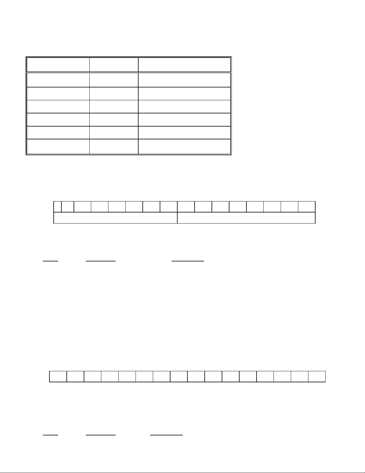
For program RAM layout refer to page 9, 11, 13
3

Model V660
V660 STRAP OPTIONS
SYNChronous/ASYNChronous (2 groups)
Normally, with either the internal clocks or a free-running external clock selected as the Base Clock, the
timing relationship between the transitions of the selected clock and the setting of the FPA bit by writing
the Control Status Register 2E16 is arbitrary. Since an asynchronous activation of the module program
through the FPA bit could result in ambiguous counting, these straps, when in the SYNC position,
synchronize the internal program activation to a safe phase of the Base Clock. This will occur (and will
be displayed on the front panel AACTIVE@LED) on the second negative-going edge of the base clock
following a write to the Control Status Register 2E16. Clock frequency division and counting will begin
on the succeeding, rising edge of the Base Clock.
If an external clock is used and it is externally gated off until after a write to the Control Status Register
2E16 (which sets FPA) is complete, the straps may be set to the ASYNC position. This is only necessary
if it is important to begin program execution and counting at the first incoming clock transitions.
Otherwise, the straps may remain in the SYNC position. AT NO TIME should these straps be in the
opposite position from one another.
FRONT PANEL INFORMATION
LEDs
ADD_REC This LED is illuminated when the operational registers are being accessed.
INT SRC This LED turns on (when Interrupts are enabled) at the end of each program step.
Inputs and Outputs
Inputs (LEMO)
TRIG 1
External trigger to proceed to next step in program. The trigger is
counted down by a predetermined count for each step. The step
takes effect at the 2nd "tick" of the base frequency clock following
the selected number of step triggers.
TRIG 2
An alternate trigger which functions identically to TRIG 1 when
selected
CLK IN
Input Base Frequency from external TTL frequency source (10
MHZ maximum)
(1MHz maximum for the V660-ZB11 option)
Outputs (LEMO)
4

Model V660
BASE CLK This output is provided to drive other Programmable Clocks from a
common frequency source.
EOL
This output is pulsed at the end of the last step (step with EOL bit
set). The purpose of this output is to permit external counting of the
number of times the list is reset (program cycles). This count could
be used to signal shutdown of the V660 after a fixed number of
cycles.
STEP
CMPL 1
This output is generated at the end of selected program steps when
the STC1 flag is set in the Program Step Flag byte.
STEP
CMPL 2
This output is generated at the end of selected program steps when
the STC2 flag is set in the Program Step Flag byte.
GATE-OUT
Latched output set or cleared at the start of each program step based
on the SGTO-bit in the Program Step Flag byte.
CLK OUT
This is the generated output clock. The clock pulse is derived from
the base clock in such a way as to minimize jitter in the clock output.
PROGRAMMING INFORMATION
VMEbus/VXIbus Addressing
Of the defined VXIbus Configuration Registers, the V660 implements those required for register-based
devices. The V660 also contains a set of Operational Registers to monitor and control the functional
aspects of the devices. Both registers sets are described in this section.
Access to the Configuration Registers for all VXIbus modules is available through the VMEbus short
address space. The register addresses are located in the upper 16 kilobytes of the A16 address range
(C000 hex to FFFF hex). The setting of the Logical Address switch, or the contents of the Logical
Address Register (see below) are mapped into Address lines A6 through A13, thereby establishing a base
address for the module somewhere in the range of C000 hex to FFC0 hex.
VXIbus Configuration Registers
Configuration Registers are required by the VXIbus specification so that the appropriate levels of system
configuration can be accomplished. The Configuration Registers in the V660 are offset from the base
address. Note: the V660 only responds to these addresses if the Short Nonprivileged Access (29 hex)
or Short Supervisory Access (2D hex) Address Modifier Codes are set for the backplane bus cycle.
Table 1 shows the applicable Configuration Registers present in the V660, their offset from the base
(Logical) address, and their Read/Write capabilities.
TABLE 1 - CONFIGURATION REGISTERS - SHORT I/O ADDRESS SPACE
OFFSET (HEX)
W/R MODE
REGISTER NAME
5

Model V660
OFFSET (HEX)
W/R MODE
REGISTER NAME
0016
W/R
ID/Logical Address Register
0216
R
Device Type Register
0416
W/R
Status/Control Register
0616
W/R
Offset Register
0816
R
Attribute Register
1E16
R
Subclass Register
ID/Logical Address Register
1
5
1
4
13
12
11
10
09
08
07
06
05
04
03
02
01
00
0016
0
1 0 0 1 1 1 1 0 0 1 0 1 0 0 1 R
DON=T CARE
LOGICAL ADDRESS REGISTER
W
D16
On READ transactions:
Bit(s) Mnemonic Description
15, 14 Device Class This is a Register-Based device.
13, 12 Address Space Needs This module requires the use of A16/A24 address space.
11 – 00 Manufacturer's ID 3881 (F2916) for KineticSystems.
For WRITE transactions, bits 15 through 8 are not used, and setting them has no effect on the V660. In
Dynamically configured systems (i.e., the Logical Address switches were set to a value of 255), bits 7
through 0 are written with the new Logical Address value.
Device Type
15
14
13
12
11
10
09
08
07
06
05
04
03
02
01
00
0216 1 1 1 1 0 1 1 0 0 1 1 0 0 0 0 0 R
On READ transactions:
6
Bit(s) Mnemonic Description

Model V660
15 - 12 Required Memory The V660 requires 256 bytes of additional memory space.
11 – 00 Model Code Identifies this device as Model V660 (66016).
Status/Control Register
15 14 13 12 11 10 09 08 07 06 05 04 03 02 01
00
┌───────┬─────┬─────┬───────┬─────────────────────────────────────────┬─────┬─────┬─────┬──
───┐
│A24 ACT│MODID│S │1 │ZEROs │RDY │PASS │0
│RST │
├───────┼─────┼─────┼───────┼─────────────────────────────────────────┴─────┴─────┴─────┼──
───┤
│A24 ENA│N/U │N/U │1 │NOT USED
│RST │
└───────┴─────┴─────┴───────┴───────────────────────────────────────────────────────────┴──
───┘
0416
Bit(s) Mnemonics Description
15 A24 Writing a "1" will enable A24 addressing and allow access to the
Operational Registers. Reading a "1" indicates A24 is active.
This bit is reset to a "0" on power-up or the assertion of
SYSRESET*.
14 MODID This Read-Only bit is set to a "1" if the module is not selected
with the MODID line on VXIbus connector P2. A "0" will
indicate that the device is selected by a high state on the P2
MODID line.
13 Status This Read-Only bit indicates the status of the last operational
transaction to the V660. A "1" indicates the transaction
completed successfully.
12 1 This Read/Write bit is included for compatibility with other
KineticSystems VXIbus modules. It should always be written
with a "1".
11-4 N/U Not used. Read as a "0".
3 RDY READY. The V660 is always ready. Read as "1".
2 PASS PASS. The V660 will always pass self tests. Read as "1".
7
1 N/U NOT USED. Read as "0".

Model V660
0 RST RESET. This Read/Write bit controls the Soft Reset condition
within the V660. While the Soft Reset condition is enabled (by
writing a "1" to this bit position), any further access to the
Operational Registers (see below) except the Diagnostic and
Interrupt Status registers is inhibited. The output bit patterns
from the module are maintained in the state they were in just
prior to the Soft Reset being enabled. This bit can be reset by
writing a "0", on power-up or the assertion of SYSRESET*.
Offset Register
15 14 13 12 11 10 09 08 07 06 05 04 03 02
01 00
┌──────────────────────────────────────────────────────────────────────────────────────────
─────┐
│A24
<───────────────────────────────────────────────────────────────────────────────────> A9 │
W/R
└──────────────────────────────────────────────────────────────────────────────────────────
─────┘
0616
This 16-bit read/write register defines the base address of the A24 Operational Registers. The register is
reset to an all "0" condition on power-up or the assertion of SYSRESET*, and is written with the
appropriate value under program control.
Attribute Register
15 14 13 12 11 10 09 08 07 06 05 04 03 02
01 00
┌──────────────────────────────────────────────────────────────────────────────┬────┬─────┬
─────┐
│NOT USED │0 │
1 │0 │R
└──────────────────────────────────────────────────────────────────────────────┴────┴─────┴
─────┘
0816
Bits 3-15: Not Used. Read as zeros
Bit 2 = 0 Indicates Interrupt Control Capability
Bit 1 = 1 Not an Interrupt Handler
Bit 0 = 0 Indicates Interrupt Status Capability
Subclass Register
15 14 13 12 11 10 09 08 07 06 05 04 03 02
01 00
8

Model V660
┌─────┬─────┬─────┬─────╥─────┬─────┬─────┬─────╥─────┬─────┬─────┬─────╥─────┬─────┬─────┬
─────┐
│1 │1 │1 │1 ║1 │1 │1 │1 ║1 │1 │1 │1 ║1 │1 │
1 │0 │R
└─────┴─────┴─────┴─────╨─────┴─────┴─────┴─────╨─────┴─────┴─────┴─────╨─────┴─────┴─────┴
─────┘
1E16
Bit 15 = 1 Indicates that this is a VXIbus-defined Extended Device
Bits 14-0 = 7FFE16 Indicates that this is an Extended Register Based Device
TABLE 2 - V660 OPERATIONAL REGISTERS - STANDARD ADDRESS SPACE
A24
OFFSET
W/R
MODE
REGISTER NAME
0016
W/R
Diagnostic Register
0216
R
Interrupt Status Register
1216
R
Reads the Control Status Register
(CSR)
1616
R
Reads the Previous Pulse Count
Register
Bits 0-15 LOW
1816
R
Reads the Previous Pulse Count
Register
Bits 16-23 HIGH
1A16
R
Reads the Current Pulse Count Register
Bits 0-15 LOW
1C16
R
Reads the Current Pulse Count Register
Bits 16-23 HIGH
1E16
R
Reads the RAM Address Pointer (RAP)
2216
R
Reads the RAM at Selected Address and
Increment Address (FSD)
2616
R
Test the Interrupt Request
2A16
W
Clears Interrupt Status
2E16
W
Writes the Control Status Register
(CSR)
3216
W
Writes the Program RAM Address
egister (RAP)R
3616
W
Writes the RAM at Selected Address and
Increment Address (FSD)
3A16
W
Disables Interrupts
3E16
W
Resets the Program Counter
4216
W
Steps the Program Counter (sync with
2nd base clock tick)
4616
W
Places the module in Inactive state,
clears Interrupt, Interrupt Request,
nhibit, and CSR RegisterI
4A16
W
Enable Interrupt
4E16
R
Tests the Interrupt
OPERATIONAL REGISTERS
9

Model V660
The Operational Registers are the means to access the functional registers of the V660. For compatibility with
other KineticSystems VXIbus modules in this series, these registers are positioned in the VMEbus Standard
Address (A24) space. The base address for these registers is defined by the contents of the Offset Register
within the Configuration Register set.
Prior to gaining access to the Operational Registers, the A24 Enable bit (bit 15) must be set in the
Status/Control Register. Note: The V660 will only respond to these addresses if the Standard
Nonprivileged Data Access (39 hex), Standard Nonprivileged Program Access (3A hex), Standard
Supervisory Data Access (3D hex), or Standard Supervisory Program Access (3E hex) Address
Modifier Codes are set for the bus cycle(s).
Of the 256 bytes requested by the setting of the Device Type register in the Configuration Register set, only
40 bytes are used. (256 is the minimum number of bytes that can be requested through the Device Type
register.) Table 2 shows the applicable Operational Registers present in the V660, their offset from the base
A24 address, and their Read/Write capabilities.
Diagnostic Register
15
14
13
12
11
10
09
0
8
07
0
6
05 04
03
02
01 00
Don=t Care
D
S 0
INT
ENA
IN
T
SR
C
D/
C 0 0
R
Don=t Care 0
0 0
INT
ENA 0
D/
C
CL
R
INI
T
W
0016
Bit Mnemonic Description
15-8 D/C Don't Care. Read as "0".
7 Diagnostic When this bit is set to a "1", the last register access to the
operational registers was valid.
6 Status When this bit is set to a "1", the last register access to the
operational registers was accepted.
5 N/U Not Used. Read as "0".
4 INT ENA Interrupt Enable: setting this bit to a "1" will enable interrupts.
3 INT SRC Interrupt Source: When this bit is set to a "1", the VXI module has
asserted an Interrupt.
10

Model V660
2 D/C Don't care. Read as "0".
1 CLR Setting this bit will clear the interrupt status bits.
0 INIT Setting this bit to a one will only reset the operational registers
(OFFSET 1216 through 4E16). The configuration registers and the
Diagnostic register are unaffected.
Interrupt Status/ID Register 0216
15 14 13 12 11 10 09 08 07 06 05 04 03 02 01
00
┌───────────────────────────────────────────────┬──────────────────────────────────────────────
─┐
│STATUS │ID
│R
└───────────────────────────────────────────────┴──────────────────────────────────────────────
─┘
0216
This is a read only 16-bit Interrupt Status Register. During an interrupt acknowledge cycle, this register will
output a Status/ID value during a D8, D16, or a D32 data transfer. In a D32 data transfer, the upper 16-bits
will be pulled up to logic A1@by the backplane termination networks. A read from this register will show the
current Status/ID value.
Bit Mnemonic Description
15-8 STATUS: These eight bits will indicate Request True or Request False:
Request True = FD16
Request False = FC16
7-0 ID: These eight bits represent the Logical Address of the V660
Configuration Registers.
Frequency Step Data (FSD)
This register provides access to the Program RAM at the address pointed to by the RAM Address Pointer
Register (RAP). Reads and Writes to the Frequency Step Data register automatically increments the RAP
register. The FSD can only be accessed when the V660 is in the inactive state.
To load a frequency step sequence, the RAM Address Pointer (RAP) is written with an appropriate starting
address (typically 0), followed by sequential 16 bit writes to the FSD with a program sequence in the order of
Modulo-N Bits 0-15, Flag bits 0-7, Count Bits 0-15, and Count Bits 16-23.
Program RAM Layout
11

Model V660
The program RAM is a 1K x 16 Static RAM. Program steps are configured as follows in the RAM:
Rap+0
Modulo-N bits 0-15 (Nf)
Rap+1
0 0 0 0 0 0 0 0
Flag bits 0-7
Rap+2
Count bits 0-15 (Np)
Rap+3
0 0 0 0 0 0 0 0
Count bits 16-23 (NP)
Frequency Step Data (FSD)
1
5
1
4
13
12
11
10
09
08
07
06
05
04
03
02
01
00
FSDW
FSDR
RAP
Modulo-N Bits 0-15
3616
2216
Frequency Word Base Clock/Desired Freq = Module-N-Value
15-08 07 06 05 04 03
02
01
00
FSD
W
FSDR
RAP
+1
Not Used
EOL
DFLG
SGT0
LAMF
STC2
STC1 TS
3616
2216
Flag Word
BIT
MNEMONIC
DESCRIPTION
15-8
Not Used
Write As Zero
7
EOL
End of List (This flags the last item in the list.)
6
DFLG
Delay Flag = 1 Disables CLK-OUT for step duration
5
SGTO
Set Gate Out (Inhibit)
4
LAMF
Set Interrupt at end of step
3
STC2
Generate Step Complete Strobe STC-2 at end of step
2
STC1
Generate Step Complete Strobe STC-1 at end of step
1-0
TS
Trigger Select
Equals 0 Software only (Note 3)
Equals 1 Output Pulse Count reached (Note 1)
Equals 2 External Step Trigger - 1
Equals 3 External Step Trigger - 2 (Note 2)
1. A programmed number of output clock pulses (COUNT).
12

Model V660
2. Front Panel LEMO "step" pulses (TRIG 1 or TRIG 2 rising edge TTL triggers) or
Normally Closed (to ground) contact closures.
3. Software only. (Read register 4216)
Note: A step can always be terminated by a read of register 4216.
15
14
13
12
11
10
09
08
07
06
05
04
03
02
01
00
FSD
W
FSDR
RAP
+2
Count Bits Low 0-15
3616
2216
Output Pulse Low This register combined with output pulse high produces the total number of
desired output pulse.
15
14
13
12
11
10
09
08
07
06
05
04
03
02
01
00
FSD
W
FSDR
RAP
+3
Don=t Care
Count Bits High 16-23
3616
2216
Output Pulse High
RAM Address Pointer (RAP)
1
5
14
13
12
11
10
09
0
8
07
06
05
04
03
02 01
00
1E
16
Not Used
R1
0
R
9
R8
R7
R6
R5
R4
R3
R2
R
1
R
32
16
Don=t Care
W1
0
W
9
W8
W7
W6
W5
W4
W3
W2
W
1
W
In the inactive state, this register serves as an address register for loading a frequency step program into
RAM. It is associated with the Frequency Step Data register (FSD) and is incremented following a read
or write to the FSD. This register can be read any time and written only when the V660 is in the inactive
state. This register is used for reading or writing a program sequence into the V660 RAM. It may also be
used to define an arbitrary starting point in a list.
In the active state, this register provides the address of the next program step. Note: Each frequency step
starts on a quad-word boundary (0, 4, 8, 12, ...).
Control Status Register (CSR)
1
5
14
13
12
11
10
09
0
8
07
06
05
04
03
02 01
00
13

Model V660
12
16
Not Used
R
2E
16
Don=t Care
FP
A
RC
M
EI
NH
SG
O
CG
O
D2
56
CSEL
W
BIT
MNEMONIC
DESCRIPTION
15-8
Not Used
Read As Zero
7
FPA
Frequency Program Active: This flag is set whenever the
frequency step program is active (read). To start V660 -
Set FPA = 1 (write), and FPA = 0 to STOP.
6
RCM
Equals 1 Set Recycle Mode (read/write bit)
5
EINH
Equals 1 Enable Inhibit when Gate-Out is true
4
SGO
Equals 1 Set Gate-Out true (initialize Gate-Out)
3
CGO
Equals 1 Clear Gate-Out
2
D256
Equals 1 Divide Base Clock selected by CSEL bits by 256
1-0
CSEL
Equals 0 (10.00 MHZ internal clock/l.0 MHZ for ZB11)
Equals 1 (10.24 MHZ internal clock/1.024 MHZ for ZB11)
Equals 2 (external clock)
Previous Pulse Count Register (PPC)
1
5
14
13
12
11
10
09
0
8
07
06
05
04
03
02
01
00
16
16
R
1
6
R1
5
R1
4
R1
3
R1
2
R1
1
R1
0
R
9
R8
R7
R6
R5
R4
R3
R2
R1
L
o
18
16
Not Used
R2
4
R2
3
R2
2
R2
1
R2
0
R1
9
R1
8
R1
7
H
i
This is a 24 bit register. To read all 24 bits of the Previous Pulse Count Register (PPC), a read from the
LOW register must be executed first followed by a read from the HIGH register. The LOW register will
return bits 1 through 16, while the HIGH register will return bits 17 through 24.
The Previous Pulse Count Register contains the number of clock output pulses generated by the previous
step. Since by design the Programmable Clock can generate an indeterminate number of clocks on a
given step, in some applications it may be necessary to be able to determine the number of clocks
generated.
14

Model V660
Current Pulse Count Register (CPC)
15
14
13
12
11
10
09
0
8
07
06
05
04
03
02
01
00
1A1
6
R1
6
R1
5
R1
4
R1
3
R1
2
R1
1
R1
0
R
9
R8
R7
R6
R5
R4
R3
R2
R1
L
o
1C1
6
Not Used
R2
4
R2
3
R22
R2
1
R2
0
R1
9
R18
R1
7
H
i
This is a 24-bit register. To read all 24 bits of the Current Pulse Count Register (CPC), a read from the LOW
register must be executed first followed by a read from the HIGH register. The LOW register will return bits
1 through 16, while the HIGH register will return bits 17 through 24.
The Current Pulse Count Register contains a count of the number of clock output pulses generated so far by
the current step. When CPC = Np and termination on number of pulses is selected, the program step occurs.
This register is required so that software can determine the current state.
15

Model V660
V660 REGISTER LAYOUT
CONFIGURATION REGISTERS
ID/Logical Address Register
1
5
1
4
13
12
11
10
09
08
07
06
05
04
03
02
01
00
0016
0
1 0 0 1 1 1 1 0 0 1 0 1 0 0 1 R
DON=T CARE
LOGICAL ADDRESS REGISTER
W
D16
Device Type
1
5
1
4
13
12
11
10
09
08
07
06
05
04
03
02
01
00
1
1 1 1 0 1 1 0 0 1 1 0 0 0 0 0 R
D16
0216
Status/Control Register
15 14 13 12 11 10 09 08 07 06 05 04 03 02 01
00
┌───────┬─────┬─────┬───────┬─────────────────────────────────────────┬─────┬─────┬─────┬─────┐
│A24 ACT│MODID│S │1 │ZEROS │RDY │PASS │0 │
RST │R
├───────┼─────┼─────┼───────┼─────────────────────────────────────────┴─────┴─────┴─────┼─────┤
│A24 ENA│N/U │N/U │1 │NOT USED │
RST │W
└───────┴─────┴─────┴───────┴───────────────────────────────────────────────────────────┴─────┘
0416
Offset Register
15 14 13 12 11 10 09 08 07 06 05 04 03 02
01 00
┌──────────────────────────────────────────────────────────────────────────────────────────
─────┐
│A24
<─────────────────────────────────────────────────────────────────────────────────> A9 │
W/R
└──────────────────────────────────────────────────────────────────────────────────────────
─────┘
16

Model V660
0616
Attribute Register
15 14 13 12 11 10 09 08 07 06 05 04 03 02
01 00
┌──────────────────────────────────────────────────────────────────────────────┬────┬─────┬
─────┐
│NOT USED │0 │
1 │0 │R
└──────────────────────────────────────────────────────────────────────────────┴────┴─────┴
─────┘
0816
Subclass Register
15 14 13 12 11 10 09 08 07 06 05 04 03 02
01 00
┌─────┬─────┬─────┬─────╥─────┬─────┬─────┬─────╥─────┬─────┬─────┬─────╥─────┬─────┬─────┬
─────┐
│1 │1 │1 │1 ║1 │1 │1 │1 ║1 │1 │1 │1 ║1 │1 │
1 │0 │R
└─────┴─────┴─────┴─────╨─────┴─────┴─────┴─────╨─────┴─────┴─────┴─────╨─────┴─────┴─────┴
─────┘
1E16
OPERATIONAL REGISTERS
INTERRUPT REQUEST REGISTER
1
5
14 13 12 11 10 09 08 07 06 05 04 03 02 01 00
2616
R
A read of this register will test the Interrupt Request.
CLEAR INTERRUPT STATUS
1
5
14 13 12 11 10 09 08 07 06 05 04 03 02 01 00
2A16
S
R
S = Status bit in Diagnostic Register = 1
A read of this register will clear the interrupt status.
17

Model V660
2E (See offset 12) page 9, 11, 13 Control Status Register
32 (See offset 1E) page 9, 11, 13 RAM Address Pointer
36 (See offset 22) page 9, 11, 13Program RAM Layout
DISABLE INTERRUPTS
1
5
14 13 12 11 10 09 08 07 06 05 04 03 02 01 00
3A16
R
A read of this register disables the interrupt.
PROGRAM COUNTER RESET
1
5
14 13 12 11 10 09 08 07 06 05 04 03 02 01 00
3e16
R
A read of this register will reset the program counter.
STEP PROGRAM COUNTER
15 14 13 12 11 10 09 08 07 06 05 04 03 02 01 00
4216
R
A read of this register will step the program counter.
MODULE RESET
15 14 13 12 11 10 09 08 07 06 05 04 03 02 01 00
4616
R
A read of this register places the module in the Inactive state, Clears Interrupt, Interrupt Request, Inhibit,
and CSR register.
ENABLE INTERRUPT
18
1
5
14 13 12 11 10 09 08 07 06 05 04 03 02 01 00
4A
W
Table of contents
Popular Portable Generator manuals by other brands

Winco
Winco 50PTOC4-03/1 Installation and operator's manual

Generac Power Systems
Generac Power Systems QT130 overview

Powermate
Powermate WX 2200 owner's manual

Aktobis
Aktobis WDH-AP005 operating manual

Peak Scientific
Peak Scientific Infinity 1032 installation guide

Boston Scientific
Boston Scientific rezum manual

Chicago Electric
Chicago Electric 65309 Set up, operating, and servicing instructions

Firman
Firman etrailer W02983 owner's manual

Powermate
Powermate PM2000i owner's manual

LONCIN
LONCIN HomeSite Power LC5000-AS Service manual

Kärcher
Kärcher PGG 3/1 Original operating instructions

ATI Technologies
ATI Technologies SX080 instruction manual