Kitronik FM Radio KIT Owner's manual

FM RADIO KIT
GET IN TUNE WITH THIS
ES
S
ENTIAL INFORMATION
BUILD INSTRUCTIONS
CHECKING YOUR PCB & FAULT-
FINDING
MECHANICAL DETAILS
HOW THE KIT
WORKS
Version 2.
0

FM Radio Essentials
www.kitronik.co.uk/2135
Build Instructions
Before you start, take a look at the Printed Circuit Board (PCB). The components go in the side with the writing on
and the solder goes on the side with the tracks and silver pads.
Start with the eight resistors:
The text on the PCB shows where R1, R2 etc go.
Ensure that you put the resistors in the right place.
PCB Ref
Value
Colour Bands
R2 & R8
10K
Brown, black, orange
R3 & R4
100K
Brown, black, yellow
R6
4.7K
Yellow, purple, red
R7
15K
Brown, green,
orange
R9
100
Brown, black, brown
R10
1
Brown, black, gold
The ceramic disc capacitors should be soldered into the board. There are a lot of these so be careful to put them all
in the correct place. The capacitors can be identified by the text printed on them (see close up image below right). It
doesnt matter which way around the capacitor goes into the board.
Solder the voltage regulator (shown right) into the PCB where it is labelled IC2. Make sure that the
shape of the component matches the outline on the PCB.
PCB Ref
Value
Text
C1, C9, C15, C18
100nF
104
C2, C12, C19, C20
10nF
103
C3 & C5
3.3nF
332
C4, C6, C16
180pF
181
C7
39pF
39
C8
2.2nF
222
C10
330pF
331
C11
220pF
221
C13
220nF
224
C14
470pF
471
PLACE RESISTORS
1
SOLDER THE CERAMIC DISC CAPACITORS
2
SOLDER THE VOLTAGE REGULATOR
3

FM Radio Essentials
www.kitronik.co.uk/2135
Solder the Integrated Circuit (IC) holder into IC3. When putting this into the board, be sure to get it
the right way around. The notch on the IC holder should line up with the notch on the lines marked
on the PCB. Once this has been done insert the 8 pin IC into this socket, making sure that the notch
on the device matches the notch on the IC holder.
Now solder in the four electrolytic capacitors. The capacitors have text printed on the side that indicates their value.
The capacitors are placed as follows.
PCB Ref
Value
C21
100
F
C23
220
F
C17 and C22
470
F
Make sure that the capacitors are the correct way around. The capacitors have a - sign marked on them, which
should match the same sign on the PCB.
Solder the two potentiometers into the PCB. Each potentiometer has a different value so they have
to be put in the correct place. If you look at the potentiometers, you will see they are labelled with
their value. The shaft of the potentiometer should point away from the PCB.
PCB Ref
Value
R1
10K
R5
100K
Solder the PP3 battery clip to the terminals labelled Power In. Connect the red wire to + and the
black wire to - after feeding it through the strain relief hole.
Solder the length of single core wire to the terminal labelled Antenna. You will first have to strip off a piece of the
insulation to expose a short length of the wires core. Before doing this, make sure that you feed it through the strain
relief hole. Once soldered, measure 750mm of wire from the point where the wire is soldered and cut any remainder
off (this will make sure that the antenna is the right length to pick up the correct radio frequencies for the radio).
SOLER THE IC HOLDER
4
SOLER THE ELECTROLYTIC CAPACITORS
5
SOLER THE
POTENTIOMETERS
6
Value
ATTACH THE BATTERY CLIP
7
CONNECT THE WIRES
8

FM Radio Essentials
www.kitronik.co.uk/2135
The kit is supplied with ½ a metre of twin cable. This cable is used to connect the speaker. Cut this
to the required length for your enclosure design.
Take the piece of wire that you have cut off and strip the ends of the wire. Connect one end to the
two terminals on the speaker (shown right) and the other end to the board marked speaker after
feeding it through the strain relief hole. It does not matter which way around these connections go.
Checking Your FM Radio PCB
Check the following before you connect any batteries for you radio.
Check the bottom of the board to ensure that:
All holes (except the four large mounting holes) are filled with the lead of a component.
All these leads are soldered.
Pins next to each other are not soldered together.
Check the top of the board to ensure that:
The outline of components IC2 and IC3 match the outlines on the PCB.
The negative markings on the electrolytic capacitors line up with the same markings on the PCB.
The red wire on the PP3 lead is connected to the power connector labelled Red and the black wire on the
PP3 lead is connected to the power connector labelled Black.
Additionally check that the resistors and capacitors are in the correct place if your board does not work.
CONNECT THE SPEAKER
9

FM Radio Essentials
www.kitronik.co.uk/2135
Adding an On / Off Switch
If you wish to add a power switch, dont solder both ends of the battery clip directly into the board, instead:
Solder one end of the battery clip to the PCB, either black to - or red to +.
Solder the other end of the battery clip to the on / off switch.
Using a piece of wire, solder the remaining terminal on the on / off switch to the remaining
power connection on the PCB.
1
2
3

FM Radio Essentials
www.kitronik.co.uk/2135
Designing the Enclosure
When you design the enclosure, you will need to consider:
The size of the PCB (below left, height including components = 22mm).
How big the battery (or batteries) are.
How to mount the speakers (below right).
All dimensions in mm.
The volume and tuning potentiometer shafts can be cut to the required length and are designed to be mounted
using a 7mm diameter hole. Maximum panel thickness is 4.5mm (allows 2mm for nut and washer on
potentiometers). The potentiometers can be mounted off board and connected to the PCB using lengths of wire if
required.
Mounting the PCB to the
enclosure
The drawing to the left
shows how a hex spacer
can be used with two bolts
to fix the PCB to the
enclosure.
Your PCB has four
mounting holes designed to
take M3 bolts.
88
46
4 x 3.3mm diameter mounting holes
4
4
Power input Antenna
Speaker
20
40.5 28 19.5
6.5

FM Radio Essentials
www.kitronik.co.uk/2135
How the FM Radio Works
To aid the description of the circuit, we have split it into two parts. The first deals with the decoding of the FM radio
signal and the second deals with the audio amplification.
Radio decoding
For the radio circuit to work, it needs a stable power supply (not one that falls as the battery becomes flat). To
provide the stable power supply, a voltage regulator is used. This provides a 3V output for the circuit to run from.
Capacitor C17 is to remove any unwanted noise from this 3V supply.
The key component of the radio circuit is the TDA7010T chip. This chip is used to receive radio signals via an aerial
and then decodes this signal to recover the audio signal that it carries. To recover the radio signal the chip needs to
generate another radio signal by using a circuit called VCO (voltage controlled oscillator) which it mixes with the
received radio signal to recover the desired radio station. The signal that the VCO generates can be altered, allowing
radio stations on different frequencies to be recovered. The VCO uses a resonant circuit that is made up of inductor
(L1), capacitor (C16) and the varicap diode (D1). A varicap diode is a diode that also has a capacitance. This
capacitance varies as the voltage across the diode varies. By adjusting the potentiometer (R5), which is used to tune
the circuit, the voltage that is fed to the varicap diode can be adjusted. This, in turn, changes the capacitance of the
varicap diode and, therefore, the frequency of the resonant circuit (and thus the frequency to which the radio is
tuned).
The remaining capacitors are used by the chip to filter the recovered radio signal.
Resistor R2 is used to disable the mute feature of the chip. If this is not fitted when the radio is not tuned into a radio
station, the audio output is muted (silent). When it is fitted you get a hissy sound between stations. We have fitted
it as it makes it easier to manually tune into stations.
Potentiometer R1 is used to control the amount of the audio output signal that is fed to the amplifier circuit. By
doing this, it will therefore control the overall volume that comes out of the radio.
Battery
(15V max)
C17
470uF
Audio
out
C20
10nF
R6
4.7K
TDA7010T
Mute
Audio out
LF
V+
Voltage
regulator
In Out
Gnd
VCO
Mix1
Mix2
Mix Out
CR
DM
Gnd
IF
Mix 3
RF in
IF
IF
R7
15K
R5
100K
Tune R4
100K D1
L1
56nH
C16
180pF
R1
10K
Volume
C12
10nF
C19
10nF
Aerial
R2
10K
C1
C2
C4
C3
C11
C10
C9
C8
C7
C6
C5

FM Radio Essentials
www.kitronik.co.uk/2135
Audio amplification
The audio amplification is performed by another Integrated Circuit or IC called a TBA820M. Inside the TBA820M are
lots of transistors, which are connected together to allow the small input signal to be amplified into a more powerful
output that can drive a speaker.
All amplifiers need to use feedback to ensure that the amount of gain stays the same. This allows the output to be an
exact copy of the input, just bigger. The gain is the number of times bigger the output is compared to the input, so if
an amplifier has a gain of 10 and there is 1 volt on the input, there will be 10 volts on the output. Before looking at
how the feedback works, we first need to understand how a standard amplifier works. An operational amplifier has
two inputs, these are called the inverting (-) and non-inverting (+) inputs. The output of the operational amplifier is
the voltage on the non-inverting input, less the voltage on the inverting input, multiplied by the amplifiers gain. In
theory, an operational amplifier has unlimited gain so if the non-inverting input is a fraction higher than the inverting
input (there is more + than -), the output will go up to the supply voltage. Change the inputs around and the output
will go to zero volts. In this format the operational amplifier is acting as a comparator: it compares the two inputs
and changes the output accordingly.
With an infinite gain the amplifier is no good to amplify audio, which is where the
feedback comes in. By making one of the input a percentage of the output the
gain can be fixed, which allows the output to be a copy of the input but bigger.
Now when the two inputs are compared and the output is adjusted, instead of it
going up or down until it reaches 0 volts or V+, it stops at the point when the two
inputs match and the output is at the required voltage.
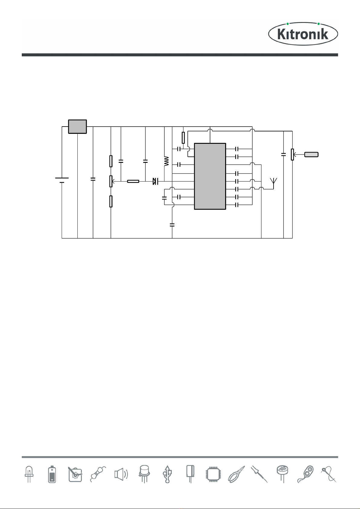
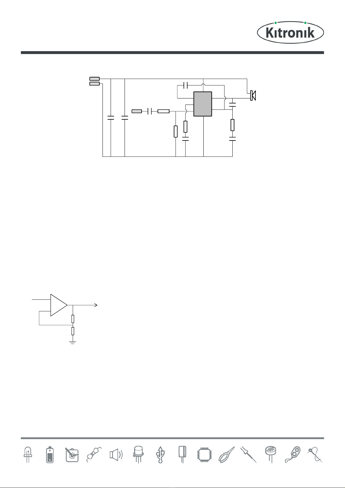
Looking at the circuit diagram for the audio amplifier, its not obvious where the feedback is this is because inside
the IC is a 6K resistor between the Output pin and the Gain setting input pin. The internal 6K resistor and the 100
resistor (R9) on the gain setting pin make up a potential divider that feeds back approximately a sixtieth of the
output. This fixes the gain so that the output is about 60 times bigger than the input.
The rest of the components are needed as follows:
C13 removes any DC offset from the audio signal from the radio IC.
R3 and R8 reduce the audio signal from the radio slightly so that when it is at full volume there is less chance of any
distortion on the sound from the speaker.
C18 & C22 are connected across the supply to make sure it remains stable.
The other capacitors have a filtering role, either to cut out high frequency noise or get the best out of the speaker.
Battery voltage
Speaker 1
R3
100K
C22
470uF
Audio
input
C21
100uF
C14
470pF
C15
100nF
R8
10K
R10
1R
TBA820M
Output
BS
FC
Gain
C18
100nF
C13
220nF
R9
100R
C23
220uF
Input
+
-
90%
Input
10%
Output
Amplifier
X10 gain

Online Information
Two sets of information can be downloaded from the product page where the kit can also be reordered from. The
Essential Information contains all of the information that you need to get started with the kit and the Teaching
Resources contains more information on soldering, components used in the kit, educational schemes of work and so
on and also includes the essentials. Download from:
www.kitronik.co.uk/2135
Every effort has been made to ensure that these notes are correct, however Kitronik accept no responsibility for
issues arising from errors / omissions in the notes.
Kitronik Ltd - Any unauthorised copying / duplication of this booklet or part thereof for purposes except for use
with Kitronik project kits is not allowed without Kitroniks prior consent.
This kit is designed and
manufactured in the UK by Kitronik
Table of contents
Other Kitronik Control Unit manuals
Popular Control Unit manuals by other brands

ITT
ITT McDonnell & Miller 14-B Series Installation & maintenance instructions

Simplex
Simplex 4100-5101 installation instructions

Advantech
Advantech ADAM-3656 Startup manual

GRAUPNER
GRAUPNER 34002 manual

ELCOS
ELCOS CIM-131 Instruction and user's manual

American Standard
American Standard 6047.8 Series installation instructions

Supermicro
Supermicro MicroBlade MBI-6118G-T41X user manual

Crestron
Crestron FT2A-PWR-UN-1-C14 installation guide

ZURN
ZURN 350AST Series installation instructions

Protector
Protector AS-5020.3 operating instructions

Weidmüller
Weidmüller DPA/DCV operating instructions

Festo
Festo MS6-SV-...-C series operating instructions