Kitronik 2112 User manual

LIGHT ACTIVATED SWITCH
CONTROL ELECTRONIC CIRCUITS WITH THE OUTPUT OF THIS
TEACHING RESOURCES
INTRODUCTION
TECHNICAL SPECIFICATION
COMPONENT FACTSHEETS
HOW TO SOLDER GUIDE
Version 3.0

Light Activated Switch Teaching Resources
www.kitronik.co.uk/2112
Index of Sheets
TEACHING RESOURCES
Index of Sheets
Introduction
Technical Specification
Soldering in 8 Steps
Resistor Values
Sensing Light – Photodetectors
Using a Transistor as a Switch
Darlington Pair
ESSENTIAL INFORMATION
Build Instructions – Light Activated
Build Instructions – Dark Activated
Checking Your Circuit
Testing the PCB
How the Light Switch Works – Dark Activated
How the Light Switch Works – Light Activated
Applications
Online Information

Light Activated Switch Teaching Resources
www.kitronik.co.uk/2112
Introduction
About the project kit
Both the project kit and the supporting material have been carefully designed for use in KS3 Design and Technology
lessons. The project kit has been designed so that even teachers with a limited knowledge of electronics should have
no trouble using it as a basis from which they can form a scheme of work.
Using the booklet
This booklet is intended as an aid for teachers when planning and implementing their scheme of work.
Please feel free to print any pages of this booklet to use as student handouts in conjunction with Kitronik project
kits.
Support and resources
You can also find additional resources at
www.kitronik.co.uk.
There are component fact sheets, information on
calculating resistor and capacitor values, puzzles and much more.
Kitronik provide a next day response technical assistance service via e-mail. If you have any questions regarding this
kit or even suggestions for improvements, please e-mail us at:
Alternatively, phone us on 0845 8380781.
Technical Specification
Supply Voltage
Minimum = 3V
Maximum = 12V
A supply voltage of 3V to 5V allows for better adjustment.
Output voltage
Vout = Supply voltage less 0.9V
Output current
Maximum = 0.5A
Guidance note
You should ensure that you have a stable power source when using the output to switch on high output loads. This is
because if the power source is unable to provide enough power, this may result in a supply voltage dip and cause
output to switch off. At this point the voltage is likely to recover and turns the output on again. The output would
then be in a state where it is rapidly switching on and off.
Board dimensions (in mm)

Light Activated Switch Teaching Resources
www.kitronik.co.uk/2112
Soldering in 8 Steps
Place soldering iron tip on the pad.
Make sure the soldering iron has warmed up. If necessary use a
brass soldering iron cleaner or damp sponge to clean the tip.
Pick up the Soldering Iron in one hand, and the
solder in the other hand.
CLEAN SOLDERING IRON
2
PICKUP IRON AND SOLDER
3
HEAT PAD
4
Place the component into the board, making sure that it goes in the
correct way around, and the part sits closely against the board.
Bend the legs slightly to secure the part. Place the board so you can
access the pads with a soldering iron.
INSERT COMPONENT
1

Light Activated Switch Teaching Resources
www.kitronik.co.uk/2112
Feed a small amount of solder into the joint. The solder
should melt on the pad and flow around the component leg.
Remove the
solder, and then remove the soldering
iron.
Leave the joint to cool for a few seconds, then using a
pair of cutters trim the excess component lead.
APPLY SOLDER
5
STOP SOLDERING
6
TRIM EXCESS
7
REPEAT
8
Repeat this process for each solder joint required.

Light Activated Switch Teaching Resources
www.kitronik.co.uk/2112
Resistor Values
A resistor is a device that opposes the flow of electrical current. The bigger the value of a resistor, the more it
opposes the current flow. The value of a resistor is given in Ω (ohms) and is often referred to as its ‘resistance’.
Identifying resistor values
Band Colour 1st Band 2nd Band Multiplier x Tolerance
Silver 100 10%
Gold 10 5%
Black 0 0 1
Brown 1 1 10 1%
Red 2 2 100 2%
Orange 3 3 1000
Yellow 4 4 10,000
Green 5 5 100,000
Blue 6 6 1,000,000
Violet 7 7
Grey 8 8
White 9 9
Example: Band 1 = Red, Band 2 = Violet, Band 3 = Orange, Band 4 = Gold
The value of this resistor would be:
2 (Red) 7 (Violet) x 1,000 (Orange) = 27 x 1,000
= 27,000 with a 5% tolerance (gold)
= 27KΩ
Resistor identification task
Calculate the resistor values given by the bands shown below. The tolerance band has been ignored.
1st Band 2nd Band Multiplier x Value
Brown Black Yellow
Green Blue Brown
Brown Grey Yellow
Orange White Black
Too many zeros?
Kilo ohms and mega
ohms can be used:
1,000Ω = 1K
1,000K = 1M

Light Activated Switch Teaching Resources
www.kitronik.co.uk/2112
Calculating resistor markings
Calculate what the colour bands would be for the following resistor values.
Value 1st Band 2nd Band Multiplier x
180 Ω
3,900 Ω
47,000 (47K) Ω
1,000,000 (1M) Ω
What does tolerance mean?
Resistors always have a tolerance but what does this mean? It refers to the accuracy to which it has been
manufactured. For example if you were to measure the resistance of a gold tolerance resistor you can guarantee
that the value measured will be within 5% of its stated value. Tolerances are important if the accuracy of a resistors
value is critical to a design’s performance.
Preferred values
There are a number of different ranges of values for resistors. Two of the most popular are the E12 and E24. They
take into account the manufacturing tolerance and are chosen such that there is a minimum overlap between the
upper possible value of the first value in the series and the lowest possible value of the next. Hence there are fewer
values in the 10% tolerance range.
E-12 resistance tolerance (± 10%)
10
12
15
18
22
27
33
39
47
56
68
82
E-24 resistance tolerance (± 5 %)
10
11
12
13
15
16
18
20
22
24
27
30
33
36
39
43
47
51
56
62
68
75
82
91

Light Activated Switch Teaching Resources
www.kitronik.co.uk/2112
LDR and Phototransistor symbols are
similar, with the Phototransistor symbol
also being similar to a normal transistor
symbol.
An LDR
A Phototransistor
Sensing Light – Photodetectors
To sense light levels in electronics requires a component which is
sensitive to light. 2 types of photodetector capable of doing this are
Light Dependent Resistors (LDR) and Phototransistors.
An LDR is a component that has a resistance that falls with an increase
in the light intensity falling upon the device.
A Phototransistor is a transistor whose base is exposed to light, rather
than being wired to a pin.
As the light level increases this activates the transistor, in a similar
manner to increasing the base current of a regular transistor.
The resistance of an LDR may typically change by 4000x between
Daylight and darkness.
A Phototransistor’s gain varies with the amount of light it is exposed
to, typically from 100 to 1500
You can see that there is a large variation between these figures
depending on the light level. With appropriate circuits these changes
can be used to control other electronics.
Applications
There are many applications for photodetectors. These include:
Lightingswitch
The most obvious application is to automatically turn on a light at certain light level. An example of this could be a
street light.
Camerashuttercontrol
Photodetectors can be used to control the shutter speed on a camera. The photodetector would be used the
measure the light intensity and then set the camera shutter speed to the appropriate level.
Example
The circuit shown right shows a simple way of constructing a circuit
that turns on when it goes dark. The increase in resistance of the LDR
in relation to the other resistor, which is fixed as the light intensity
drops, will cause the transistor to turn on. The value of the fixed
resistor will depend on the LDR used, the transistor used and the
supply voltage.
Load
5v
0v
Load
5v
0v

Light Activated Switch Teaching Resources
www.kitronik.co.uk/2112
Using a Transistor as a Switch
Overview
A transistor in its simplest form is an electronic switch. It allows a small amount of current to switch a much larger
amount of current either on or off. There are two types of transistors: NPN and PNP. The different order of the
letters relate to the order of the N and P type material used to make the transistor. Both types are available in
different power ratings, from signal transistors through to power transistors. The NPN transistor is the more
common of the two and the one examined in this sheet.
Schematic symbol
The symbol for an NPN type transistor is shown to the right along with the
labelled pins.
Operation
The transistor has three legs: the base, collector and the emitter. The emitter is usually connected to 0V and the
electronics that is to be switched on is connected between the collector and the positive power supply (Fig A). A
resistor is normally placed between the output of the Integrated Circuit (IC) and the base of the transistor to limit
the current drawn through the IC output pin.
The base of the transistor is used to switch the transistor on and off. When the voltage on the base is less than 0.7V,
it is switched off. If you imagine the transistor as a push to make switch, when the voltage on the base is less than
0.7V there is not enough force to close the switch and therefore no electricity can flow through it and the load (Fig
B). When the voltage on the base is greater than 0.7V, this generates enough force to close the switch and turn it on.
Electricity can now flow through it and the load (Fig C).
Current rating
Different transistors have different current ratings. The style of the package
also changes as the current rating goes up. Low current transistors come in
a ‘D’ shaped plastic package, whilst the higher current transistors are
produced in metal cans that can be bolted onto heat sinks so that they
don’t over heat. The ‘D’ shape or a tag on the metal can is used to work out
which pin does what. All transistors are wired differently so they have to be
looked up in a datasheet to find out which pin connects where.
IC
output
Load
5V
0V
Fig A – Basic transistor circuit
LOAD
<0.7V
Fig B – Transistor turned off
LOAD
>0.7V
Fig C – Transistor turned on
Emitter
Base
Collector

Light Activated Switch Teaching Resources
www.kitronik.co.uk/2112
Darlington Pair
What is a Darlington Pair?
A Darlington Pair is two transistors that act as a
single transistor but with a much higher
current gain.
What is current gain?
Transistors have a characteristic called ‘current
gain’. This is referred to as its hFE.
The amount of current that can pass through
the load when connected to a transistor that is
turned on equals the input current x the gain
of the transistor (hFE).
The current gain varies for different transistor and can be looked up in the datasheet for the device. Typically, it may
be 100. This would mean that the current available to drive the load would be 100 times larger than the input to the
transistor.
Why use a Darlington Pair?
In some applications, the amount of input current available to switch on a transistor is very low. This may mean that
a single transistor may not be able to pass sufficient current required by the load.
As stated earlier, this equals the input current x the gain of the transistor (hFE). If it is not possible to increase the
input current, then we need to increase the gain of the transistor. This can be achieved by using a Darlington Pair.
A Darlington Pair acts as one transistor but with a current gain that equals:
Total current gain (hFE total) = current gain of transistor 1 (hFE t1) x current gain of transistor 2 (hFE t2)
So, for example, if you had two transistors with a current gain (hFE) = 100:
(hFE total) = 100 x 100
(hFE total) = 10,000
You can see that this gives a vastly increased current gain when compared to a single transistor. Therefore, this will
allow a very low input current to switch a much larger load current.
Base activation voltage
In order to turn on a transistor, the base input voltage of the transistor will (normally) need to be greater than 0.7V.
As two transistors are used in a Darlington Pair, this value is doubled. Therefore, the base voltage will need to be
greater than 0.7V x 2 = 1.4V.
It is also worth noting that the voltage drop across the collector and emitter pins of the Darlington Pair when they
turn on will be around 0.9V. Therefore if the supply voltage is 5V (as above) the voltage across the load will be will be
around 4.1V (5V – 0.9V).
Load
5v
0v
Darlington
pair
Input
Load
5v
0v
Darlington
pair
Input

LIGHT ACTIVATED SWITCH
CONTROL ELECTRONIC CIRCUITS WITH THE
OUTPUT OF THIS
ESS
ENTIAL INFORMATION
BUILD INSTRUCTIONS
CHECKING YOUR PCB & FAULT-
FINDING
HOW THE KIT
WORKS
APPLICATIONS
Version 3.0

Light Activated Switch Essentials
www.kitronik.co.uk/2112
Connecting an external circuit to the boards output
The circuit can be used to control another device. To do this the device that
is to be controlled should be connected to the terminals labelled ‘output’.
When the circuit is activated the output turns on and can be used to turn on
the device to which it is connected.
Note: This output will be around 0.9V lower that that connected to the PCB.
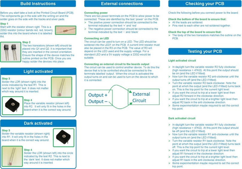
Build Instructions – Light Activated
Before you start, take a look at the Printed Circuit Board (PCB). The components go in the side with the writing on
and the solder goes on the side with the tracks and silver pads.
Start with the 220Ω resistor that is marked with red, red, brown coloured bands. Solder the
resistor into the PCB where it is labelled R4. It doesn’t matter which way around the resistor goes
into the board.
The two transistors should be placed into Q1 and Q2. It is important that they are inserted in the
correct orientation. Ensure that the shape of the device matches the outline printed on the PCB.
Solder the devices into place.
Solder the Photodetector into the circle indicated by the text R1. This is next to the ‘light’
text. For the phototransistor make sure the flat edge is towards the Power connections end
of the PCB. It does not matter which way around the LDR is inserted
Place the variable resistor into R2. It will only fit in the holes in the board when it is the correct way
around.
Connecting power
There are two power terminals on the PCB to allow power to be connected.
These are identified by the text ‘power’ on the PCB.
The positive power connection should be connected to the terminal indicated by the text ‘+’ and ‘red’.
The negative power connection should be connected to the terminal indicated by the text ‘-’ and ‘black’.
Connecting an LED
The circuit can be used to turn on an LED. The LED should be soldered into the LED1 on the PCB. A current limit
resistor must also be placed in the R3 on the PCB. The value of R3 will depend on the LED used and the supply
voltage. For a standard LED and a 5V supply voltage a 220Ω would be suitable.
SOLDER THE PHOTODETECTOR
3
PLACE RESISTOR
1
PLACE THE TRANSISTORS
2
SOLDER THE
VARIABLE RESISTOR
4
External
Circuit
Output +
Output –
LDR
Phototransistor

Light Activated Switch Essentials
www.kitronik.co.uk/2112
Build Instructions – Dark Activated
Before you start, take a look at the Printed Circuit Board (PCB). The components go in the side with the writing on
and the solder goes on the side with the tracks and silver pads.
Start with the 220Ω resistor that is marked with red, red, brown coloured bands. Solder the
resistor into the PCB where it is labelled R4. It doesn’t matter which way around the resistor goes
into the board.
The two transistors should be placed into Q1 and Q2. It is important that they are inserted in the
correct orientation. Ensure that the shape of the device matches the outline printed on the PCB. Once
you are happy, solder the devices into place.
Place the variable resistor into R1. It will only fit in the holes in the board when it is the correct way
around.
Solder the Photodetector into the circle indicated by the text R2. This is next to the ‘dark’
text. For the phototransistor make sure the flat edge is towards the Output connections
end of the PCB. If you have an LDR it does not matter which way around it is inserted.
Connecting power
There are two power terminals on the PCB to allow power to be connected.
These are identified by the text ‘power’ on the PCB.
The positive power connection should be connected to the terminal indicated by the text ‘+’ and ‘red’.
The negative power connection should be connected to the terminal indicated by the text ‘-’ and ‘black’.
Connecting an LED
The circuit can be used to turn on an LED. The LED should be soldered into the LED1 on the PCB. A current limit
resistor must also be placed in the R3 on the PCB. The value of R3 will depend on the LED used and the supply
voltage. For a standard LED and a 5V supply voltage a 220Ω would be suitable.
Connecting an external circuit to the boards output
The circuit can be used to control another device. To do this the device
that is to be controlled should be connected to the terminals labelled
‘output’. When the circuit is activated the output turns on and can be
used to turn on the device to which it is connected.
Note: This output will be around 0.9V lower that that connected to the
PCB.
SOLDER THE PHOTODETECTOR
4
Phototransistor
LDR
PLACE RESISTOR
1
PLACE THE
TRANSISTORS
2
SOLDER THE VARIABLE RESI
STOR
3
External
Circuit
Output +
Output –

Light Activated Switch Essentials
www.kitronik.co.uk/2112
Checking Your Circuit
Check the following before you connect power to the board:
Check the bottom of the board to ensure that:
All these leads are soldered.
Pins next to each other are not soldered together.
Check the top of the board to ensure that:
The body of the two transistors match the outline on the PCB.
Testing the PCB
Light activated circuit
In daylight, turn the variable resistor R2 fully clockwise (high resistance = 1MΩ). At this point the output
should be on (and the LED if fitted).
Now turn the variable resistor R2 anti-clockwise until the output turns off (and the LED if fitted).
Turn the variable resistor R2 back clockwise. Note the point at which the output (and the LED if fitted) turns
back on. This is the trip point for the current light level.
If you want the circuit to trip at a lower light level then adjust R2 forward in the clockwise direction.
If you want the circuit to trip at a brighter light level then adjust R2 back in the anti-clockwise direction.
Some experimentation maybe required to set the correct trip point.
Dark activated circuit
In daylight turn the variable resistor R1 fully clockwise (high resistance = 1MΩ). At this point the output
should be off (and the LED if fitted).
Now turn the variable resistor R1 anti-clockwise until the output turns on (and the LED if fitted).
Turn the variable resistor R1 back clockwise. Note the point at which the output (and the LED if fitted) turns
back off. This is the trip point for the current light level.
If you want the circuit to trip at a lower light level then adjust R1 forward in the clockwise direction.
If you want the circuit to trip at a brighter light level then adjust R1 back in the anti-clockwise direction.
Some experimentation maybe required to set the correct trip point.

Light Activated Switch Essentials
www.kitronik.co.uk/2112
How the Light Switch Works – Dark Activated
The circuit operation is very simple. When the input to the transistor Q1, which is fed from the connecting point of
R1 and Phototransistor, is greater than 1.4V, the output is turned on. Normally it requires 0.7V to turn on a
transistor but this circuit uses two transistors in a Darlington Pair, meaning that it requires 2 x 0.7V = 1.4V to turn on
both transistors.
When the phototransistor detects a brighter light level, current begins to flow through the component down to
ground, thus pulling the voltage down at the transistor and turning it off.
When the phototransistor detects a darker light level, the phototransistor conducts less, so that the voltage at Q1 is
pulled towards the supply voltage by the resistor R1 and R4. When this voltage is at 1.4V or higher transistor Q1
turns on.
R4 is present to protect the transistor Q1 should the variable resistor be set to zero.
It is also worth noting that the output, when turned on, will be around 0.9V lower than the supply voltage V+. This is
because of the voltage drop across the collector and emitter pins of the Darlington Pair of transistors. Therefore if
the supply voltage is 5V, then the output voltage will be around 4.1V.
Adjusting the trigger level
The point at which the circuit is triggered is set by the 1MΩ variable resistor. By varying the value of this resistor, the
ratio of current flow of R1 and the phototransistor can be varied to a point where a centre voltage (trip point) of
1.4V is achieved at the desired light level.
LED (if fitted)
If LED1 and R3 are fitted the LED will light at this point. The value of R3 should be selected for the relevant supply
voltage on LED used. A standard LED would require around 10mA (0.01A) producing a normal brightness. As stated, a
5V supply would give 4.1V across LED1 and R3. The LED1 would use 1.9V, leaving around 2.2V (4.1V-1.9V) across R3.
Using R = V/I R3 = 2.2 / 0.01 R3 = 220Ω

Light Activated Switch Essentials
www.kitronik.co.uk/2112
How the Light Switch Works – Light Activated
The circuit operation is very simple. When the input to the transistor Q1, which is fed from the connecting point of
the Phototransistor and R2, is greater than 1.4V, the output is turned on. Normally it requires 0.7V to turn on a
transistor but this circuit uses two transistors in a Darlington Pair, meaning that it requires 2 x 0.7V = 1.4V to turn on
both transistors.
The voltage at the join of the phototransistor and R2 is determined by the amount of light/darkness the
phototransistor can detect.
The variable resistor is set so that the when the phototransistor is in darkness, it pulls the voltage down to ground
and turns off the transistor. When the phototransistor illuminated it conducts, allowing more current to flow and
the voltage at the base of the transistor Q1 rises above 1.4V.
R4 is only present to protect the transistor in the dark activated version (when the variable resistor is set to zero).
It is also worth noting that the output, when turned on, will be around 0.9V lower than the supply voltage V+. This is
because of the voltage drop across the collector and emitter pins of the Darlington Pair of transistors. Therefore if
the supply voltage is 5V, then the output voltage will be around 4.1V.
Adjusting the trigger level
The point at which the circuit is triggered is set by the 1MΩ variable resistor. By varying the value of this resistor, the
ratio of current flow of R1 and the phototransistor can be varied to a point where a centre voltage (trip point) of
1.4V is achieved at the desired light level.
LED (if fitted)
If LED1 and R3 are fitted, the LED will light at this point. The value of R3 should be selected for the relevant supply
voltage on LED used. A standard LED would require around 10mA (0.01A) producing a normal brightness. As stated, a
5V supply would give 4.1V across LED1 and R3. The LED1 would use 1.9V, leaving around 2.2V (4.1V-1.9V) across R3.
Using R = V/I R3 = 2.2 / 0.01 R3 = 220Ω

Light Activated Switch Essentials
www.kitronik.co.uk/2112
Applications
Garden lamp that switches on automatically at night
As shown to the right, by simply adding a battery
holder and light bulb to a PCB built in the ‘dark
activated’ configuration, you can create a garden
light that automatically comes on in the dark.
Parts list to build 100 garden lights:
Part no.
Description
Qty
2112
Light A
ctivated
S
witch
100
2232
-
25
2 x AA
B
attery
Cage with L
eads, pack of 25
4
3517
MES Lamp H
older
(E
conomy
)
, pack of 50
2
3519
MES L
amp 2.5V, pack of 50
2
2201
-
40
Zinc Chloride AA B
atteries, box of 40
5
Drawer alarm, which sounds when a dark draw is opened
As shown to the right, by simply adding a
battery holder, switch and buzzer to a PCB
built in the ‘light activated’ configuration,
you can create an alarm that sounds when a
dark draw is opened and the PCB is exposed
to light. The switch is to allow the alarm to
be activated or deactivated.
Parts list to build 100 draw alarms:
Part no.
D
escription
Qty
2112
Light Activated S
witch
100
2232
-
25
2 x AA B
attery
Cage with L
eads, pack of 25
4
3404
Miniature DPDT S
lide
S
witch, pack of 10
10
3301
Piezo Buzz
er (with Drive), pack of 10
10
2201
-
40
Zinc Chloride AA B
atteries, box of 40
5

Light Activated Switch Essentials
www.kitronik.co.uk/2112
Line following buggy (using 2 light activated boards)
As shown below, by using two light activated boards and two motors, it is possible to make a line following buggy.
The boards just need to be mounted close to the ground with the light sensor facing down. Normally the buggy will
travel in a straight line. If one of the sensors cross the dark line, it turns off the motor on that side. This will steer the
buggy away from the line. Once it has been steered away from the line, the motor will turn back on. This circuit
could be used with Lego motors.
Parts list to build 100 buggies:
Part no.
Description
Qty
2112
Light Activated S
witch
200
2234
-
25
3 x AA B
attery
Cage with C
lip, pack of 25
4
2238
-
25
PP3 Battery Clip L
ead, pack of 25
4
2501
Motor
(Medium Torque), pack of 10
20
2505
Plastic Motor Mounting Clips, pack of 10
20
2201
-
40
Zinc Chloride AA B
atteries, box of 40
8
Note: No gear box parts included.

Online Information
Two sets of information can be downloaded from the product page where the kit can also be reordered from. The
‘Essential Information’ contains all of the information that you need to get started with the kit and the ‘Teaching
Resources’ contains more information on soldering, components used in the kit, educational schemes of work and so
on and also includes the essentials. Download from:
www.kitronik.co.uk/2112
Every effort has been made to ensure that these notes are correct, however Kitronik accept no responsibility for
issues arising from errors / omissions in the notes.
Kitronik Ltd - Any unauthorised copying / duplication of this booklet or part thereof for purposes except for use
with Kitronik project kits is not allowed without Kitronik’s prior consent.
This kit is
designed and manufactured in the UK by Kitronik
Other manuals for 2112
2
Table of contents
Other Kitronik Switch manuals
Popular Switch manuals by other brands

Brocade Communications Systems
Brocade Communications Systems FastIron SX 800 Diagnostic manual

Avocent
Avocent SwitchView 130 Quick installation guide

ubiquoss
ubiquoss E3208E installation guide

Lantech
Lantech IPGS-5424 user manual

Cisco
Cisco Catalyst 3130 reference guide

StarTech.com
StarTech.com SV431DD2DU3A quick start guide