LANGER EMV-Technik P1401 User manual

2018.03.22 User Manual P1400 P1500 Final.docx
User Manual
P1401/P1501 set
RF field coupling up to 1 GHz
P1402/P1502 set
RF field coupling up to 3 GHz
- Translation of the original user manual -
Copyright © Juni 2014
LANGER EMV-Technik GmbH

- 2 -
LANGER
EMV-Technik
DE-01728 Bannewitz
mail@langer-emv.de
www.langer-emv.com
P1401/P1501 and P1402/P1502 set
Content: Page
1Safety instructions 3
2Description of the system 5
Use 52.1
P1401 and P1402 field sources 72.2
P1501 and P1502 field sources 92.3
Measurement outputs of the field sources 112.4
D70 h10 and D70 h03 spacer rings 112.5
FKE 30 field chamber insert 112.6
EPM 02 and BPM 02 field meter 122.7
Orientation of the field sources 132.8
3Start-up and measurement 14
Measuring devices 143.1
Test board 143.2
Calibration of the measurement set-up 153.3
Measurement set-up 163.4
Measurement 173.5
4Warranty 18
5Technical Parameters 19
P1401/P1501 195.1
P1402/P1502 215.2
EPM 02 / BPM 02 field meters 235.3
6Scope of delivery of the P1401/P1501 set 24
7Scope of delivery of the P1402/P1502 set 25

- 3 -
LANGER
EMV-Technik
DE-01728 Bannewitz
mail@langer-emv.de
www.langer-emv.com
P1401/P1501 and P1402/P1502 set
1 Safety instructions
Read and follow the operating instructions carefully and keep them in a safe place for later
consultation. The devices may only be used by personnel who are qualified in the field of
electromagnetic compatibility (EMC) and who are eligible to carry out this work.
When using a product from Langer EMV Technik GmbH, please observe the following safety
instructions to protect yourself from electric shocks or the risk of injuries and to protect the devices
used and the test IC from destruction.
Use a power amplifier that is stable under open-circuit conditions and short-circuit proof.
Observe the operating and safety instructions for all devices used in the set-up.
Never use any damaged or defective devices.
Carry out a visual check before using a measurement set-up with a Langer EMV-
Technik GmbH product. Replace any damaged connecting cables before starting
the product.
Never leave a product from Langer EMV-Technik GmbH unattended whilst this is
in operation.
The Langer EMV-Technik GmbH product may only be used for its intended
purpose. Any other use is forbidden.
People with a pace-maker are not allowed to work with these devices.
The test set-up should always be operated via a filtered power supply.
Attention! Functional interference emissions (near fields and far fields) may occur when the
field sources from the P1401/P1501 set or P1402/P1502 set are operated. The user is
responsible for taking appropriate measures to protect all electronic devices used in the
course of the tests. In particular, the user is responsible for protecting the measuring
devices used for the test set-up and all other electronic devices outside the test bench
against interference emissions so that their intended function is not impaired. This can be
achieved by:
- observing an appropriate safety distance
- use of shielded rooms or enclosures (e.g. shielded tents)
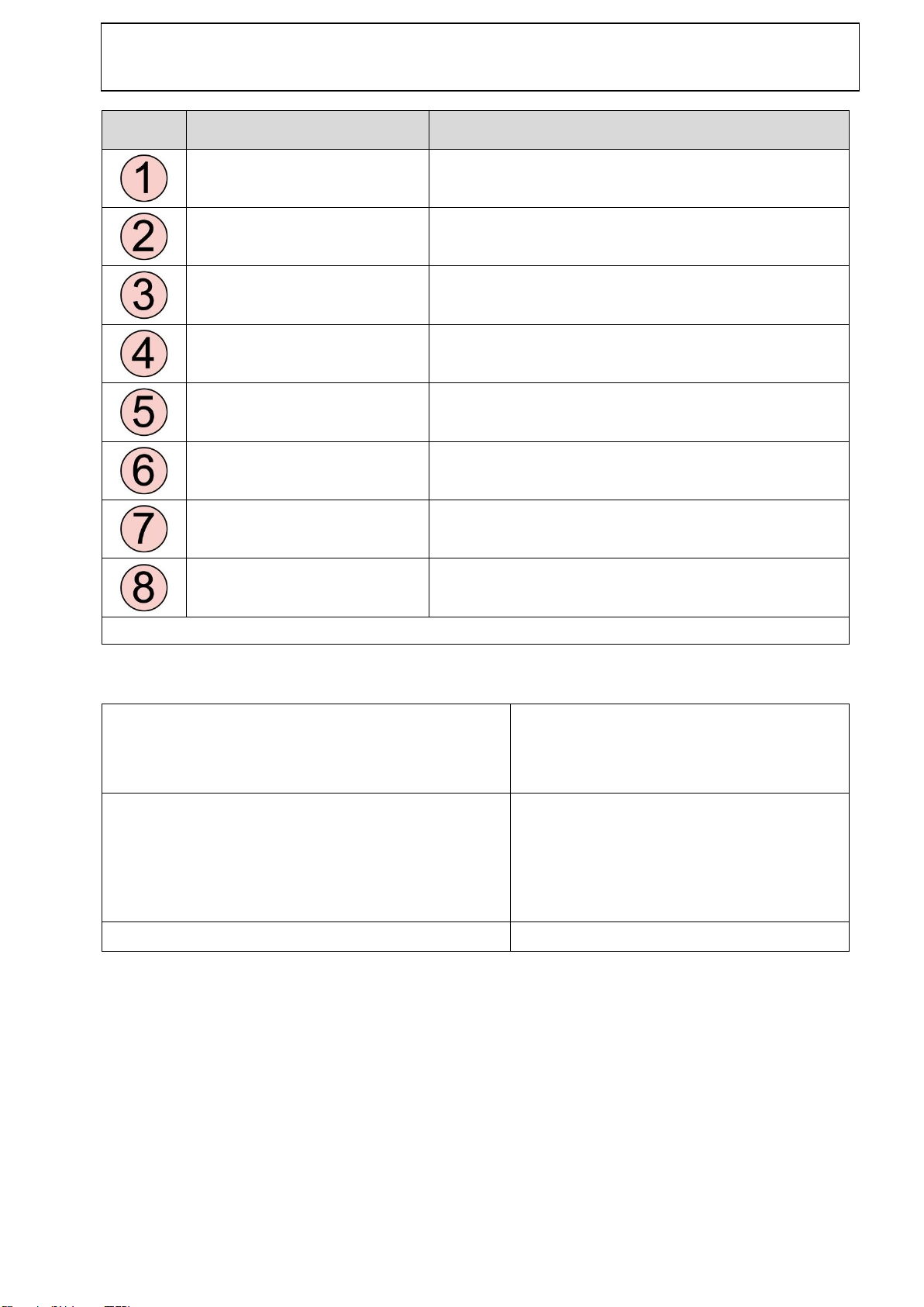
A disturbance field is generated in the field chamber of the field source when operating the
test bench. Make sure that the field chamber is not opened under any circumstances during
the test for safety reasons (hazard due to RF). The field source may only be operated with
the field chamber closed and in accordance with the measurement set-up. The test bench
has to be operated in a shielded room or enclosure.
We cannot assume any liability for damage due to improper use.
The disturbances that are injected into the modules can destroy the test IC (latch-up) if their
intensity is too high. Protect the device under test by:
- connecting a protective resistor in the IC's incoming power supply
- increasing the disturbance gradually and stopping when a functional fault occurs
- interrupting the power supply to the test IC in the event of a latch-up.

- 4 -
LANGER
EMV-Technik
DE-01728 Bannewitz
mail@langer-emv.de
www.langer-emv.com
P1401/P1501 and P1402/P1502 set
Attention! Make sure that internal functional faults are visible from outside. The test IC may
be destroyed due to an increase in the injection intensity if the faults are not visible from
outside. Take the following precautions if necessary:
monitoring representative signals in the test IC
special test software
•visible reaction of the test IC to inputs (reaction test of the test IC)
We cannot assume any liability for the destruction of test ICs!

- 5 -
LANGER
EMV-Technik
DE-01728 Bannewitz
mail@langer-emv.de
www.langer-emv.com
P1401/P1501 and P1402/P1502 set
2 Description of the system
Use2.1
The P1401/P1501 set or P1402/P1502 set can be used to measure the immunity of integrated
circuits (ICs) to magnetic and electric fields in the frequency range of up to 1 GHz and 3 GHz,
respectively.
The P1401 or P1402 field source is used to generate a magnetic test field and the P1501 or P1502
field source to generate an electric test field. The respective field source is positioned above the
test IC by using a spacer ring and its test field is then applied to the IC to measure its immunity to
disturbances.
Figure 1 shows the basic set-up for immunity measurements with the P1501 field source as an
example. The P1401/P1501 or P1402/P1502 IC test system, the ICE1
1
IC test environment as well
as different measuring and test devices
2
are required for the measurement set-up:
Note: The P1401 or P1402 field source is operated under short-circuit conditions and the P1501
or P1502 field source is operated under open-circuit conditions. Any power amplifier that is used
to supply the field sources must be designed for this purpose, i.e. it must be stable under open-
circuit conditions and short-circuit proof.
Figure 1 Basic set-up for immunity measurements using the ICE1 IC test environment and P1401/P1501
IC test system (here: P1501 field source)
1
not included in the scope of delivery
2
not included in the scope of delivery

- 6 -
LANGER
EMV-Technik
DE-01728 Bannewitz
mail@langer-emv.de
www.langer-emv.com
P1401/P1501 and P1402/P1502 set
No.
Name
Description
P1401 (P1401/P1501 set)
P1402 (P1402/P1502 set)
RF field source to generate a magnetic test field
P1501 (P1401/P1501 set)
P1502 (P1402/P1502 set)
RF field source to generate an electric test field
FKE 30
Field chamber insert (only for P1402 with D70 h10)
D70 h03
Spacer ring, 3 mm
D70 h10
Spacer ring, 10 mm
EPM 02
Field meter to measure the electric field
BPM 02
Field meter to measure the magnetic field
SMA-SMB 1 m
Measuring cable
Table 1 Brief description of the P1401/P1501 set; P1402/P1502 set
The following components, not included in the scope of delivery, are also needed:
ICE1 set, IC Test Environment
(Langer EMV-Technik GmbH)
-GND 25 ground plane
-GNDA 02 ground adapter
-CB 0708 connection board
-OA 4005 oscilloscope adapter
Measuring and test devices
-Directional coupler
-RF power amplifier
-Signal generator
-PC
-Oscilloscope
-Test IC monitoring equipment
Other
-Test board for test IC
The test board together with the test IC is inserted into the ground plane of the measurement set-
up. The field source (here P1501) is located above the test IC by using a spacer ring. A signal
generator and an RF power amplifier are used to supply the field source. A directional coupler can
be used to monitor the forward power.
An oscilloscope and PC are needed to monitor the equipment under test and/or control the
measurement set-up. The voltage present on the electrode (P1501/P1502) and/or the current
flowing through the electric conductor (P1401/P1402) can be monitored via the field sources’
measurement output.
The principal measurement process corresponds to IEC 62132-2:2010.

- 7 -
LANGER
EMV-Technik
DE-01728 Bannewitz
mail@langer-emv.de
www.langer-emv.com
P1401/P1501 and P1402/P1502 set
P1401 and P1402 field sources2.2
Figure 2 and Figure 3 show the P1401 and P1402 field source which generate a magnetic
test field. Both field sources have two plug connectors, an RF power input (N type) to power the
field source and a measurement output (SMB type) at the top. The power input is marked and
the measurement output is marked .
Figure 2 P1401 field source with 4 cm long electric
conductor
Figure 3 P1402 field source with 3 cm long electric
conductor
On the inside of the field source, the RF power input is connected to the end of the
electric conductor located at the bottom of the field source. The other end of the electric conductor
is connected to ground of the field source and thus causes a short circuit in the RF current path.
The resulting RF current generates a magnetic field that develops around the electric conductor.

- 8 -
LANGER
EMV-Technik
DE-01728 Bannewitz
mail@langer-emv.de
www.langer-emv.com
P1401/P1501 and P1402/P1502 set
Figure 4 Principle of the immunity measurement using the P1401 or P1402 field source (magnetic field)
Figure 4 shows the basic measurement principle. The field source, the spacer ring and the ground
surface with the test board form a field chamber. This field chamber limits and shields the
generated magnetic field. The FKE 30 field chamber insert has to be used in connection with the
P1402 field source.
Figure 5 FKE 30 field chamber insert for P1402 field source
A current divider (shunt) is located in the current path of the field source to measure the
field-generating current . This current can be calculated from the voltage at the field source's
measurement output (refer to section 2.4). The measurement output is terminated with 50 Ωinside
the field source.

- 9 -
LANGER
EMV-Technik
DE-01728 Bannewitz
mail@langer-emv.de
www.langer-emv.com
P1401/P1501 and P1402/P1502 set
P1501 and P1502 field sources2.3
Figure 6 and Figure 7 show the P1501 and P1502 field source which generate an electric
test field. Both field sources have two plug connectors, an RF power input (N type) to power the
field source and a measurement output (SMB type) at the top. The power input is marked and
the measurement output is marked .
Figure 6 P1501 field source
Figure 7 P1502 field source

- 10 -
LANGER
EMV-Technik
DE-01728 Bannewitz
mail@langer-emv.de
www.langer-emv.com
P1401/P1501 and P1402/P1502 set
Figure 8 Principle of the immunity measurement using the P1501 or P1502 field source (electric field)
On the inside of the field source, the RF power input is connected to the electrode located at the
bottom of the field source. Due to the potential difference between the electrode and the ground
surface, an electric field is generated which exits the electrode in the orthogonal direction.
Figure 8 shows the basic measurement principle. The field source, the spacer ring and the ground
surface with the test board form a field chamber. This field chamber limits and shields the
generated electric field.
An ohmic voltage divider is located at the electrode of the P1501 field source to measure the
field-generating voltage . This voltage can be calculated from the voltage at the field source's
measurement output (refer to section 2.4). A capacitive voltage meter is used in the P1502
field source instead to measure the field-generating voltage . The respective correction factors
are thus different (refer to section 2.4). The measurement outputs of both field sources are
terminated with 50 Ωon the inside.

- 11 -
LANGER
EMV-Technik
DE-01728 Bannewitz
mail@langer-emv.de
www.langer-emv.com
P1401/P1501 and P1402/P1502 set
Measurement outputs of the field sources2.4
The field sources' measurement outputs can be used to calculate the magnetic flux density or
electric field strength generated by the field sources at the position of the test IC.
The voltage has to be measured at the field sources’outputs for this purpose. The respective
field quantities can then be calculated using the conversion factors defined in Table 2.
P1401/P1402
P1501/P1502
Table 2 Conversion factors of the field sources to calculate the field quantities
D70 h10 and D70 h03 spacer rings2.5
The D70 h10 and D70 h03 spacer rings are part of the P1401/P1501 and P1402/P1502 IC test
systems. The spacer rings have an inner diameter d = 70 mm and a height h = 10 mm or
h = 3 mm. The spacer rings are used to position the field sources on the ground surface above the
test IC. The height of the spacer ring determines the distance between the field source and the IC.
The ground surface, the field source and the spacer ring form a field chamber in which the test field
develops.
Figure 9 D70 h03 and D70 h10 spacer rings
FKE 30 field chamber insert2.6
The FKE 30 field chamber insert is only used together with the P1402 field source and the
D70 h10 spacer ring. When using the P1402 field source, the FKE 30 field chamber insert has to
be installed at the bottom of the field source as shown in Figure 10. The field source can then be
positioned on the spacer ring. The field chamber insert is now inside the spacer ring.
The field chamber insert ensures a higher suppression of the field’s electric component.
Figure 10 FKE 30 field chamber insert for use with P1402 field source

- 12 -
LANGER
EMV-Technik
DE-01728 Bannewitz
mail@langer-emv.de
www.langer-emv.com
P1401/P1501 and P1402/P1502 set
EPM 02 and BPM 02 field meters2.7
The magnetic or electric field strength generated by the field sources at the position of the test IC
can be measured with the BPM 02 and EPM 02 field meters. To do so, a field meter has to be
inserted in the GND 25 ground plane using the GNDA 02 ground adapter. To calculate the
magnetic flux density and the electric field strength based on the voltage measured at the
output of the respective field meter, the conversion factors defined in Table 3 are used.
BPM 02
EPM 02
Table 3 Conversion factors of the BPM 02 und EPM 02 field meters
Figure 11 BPM 02 dE/dt field meter
Figure 12 EPM 02 dB/dt field meter

- 13 -
LANGER
EMV-Technik
DE-01728 Bannewitz
mail@langer-emv.de
www.langer-emv.com
P1401/P1501 and P1402/P1502 set
Orientation of the field sources2.8
Electric field:
The electric field is orthogonal to the ground surface (surface of the test IC) in the area of the
test IC (cf. Figure 13). Turning the field source on the spacer ring has no significant impact on the
direction and the intensity of the electric field. However, we recommend that the orientation is
selected for the measurement that was also used to calibrate the measurement set-up.
Please refer to section 3.2 for further information on the calibration of the measurement set-up.
Magnetic field:
The magnetic field is oriented in a plane parallel to the ground surface in the area of
the test IC (cf. Figure 14). Turning the field source on the spacer ring allows the user to vary the
magnetic field's direction in this plane. The orientation of the electric conductor is marked at the
bottom of the field source as an aid. In addition, there are two marks on the outer margin of the
field source that show the orientation of the electric conductor. These are visible in Figure 2 and
Figure 3 and can be used to adjust the orientation of the field source on the spacer ring. The
electric conductor and the magnetic field are perpendicular to each other in the area of the test IC.
Figure 13 Field coupling principle, electric field
Figure 14 Field coupling principle, magnetic field

- 14 -
LANGER
EMV-Technik
DE-01728 Bannewitz
mail@langer-emv.de
www.langer-emv.com
P1401/P1501 and P1402/P1502 set
3 Start-up and measurement
The P1401/P1501 or P1402/P1502 IC test system can be used to measure the immunity of
integrated circuits (ICs) to magnetic and electric fields in the frequency range of up to 1 GHz and
3 GHz, respectively. The immunity to electric fields and magnetic fields is measured separately.
The basic measurement set-up, the measurement princple and a description of the individual
components of the test systems can be found in section 2.
Measuring devices3.1
The ICE1 test environment and P1401/P1501 or P1402/P1502 IC test system from
Langer EMV-Technik GmbH are used to carry out immunity measurements. In addition, the
following devices are needed for the measurement set-up:
Signal generator to generate a test signal
RF power amplifier to generate the required power
Directional coupler (optional) to measure the forward and reverse power
Spectrum analyzer (optional) to monitor the signal at the measurement output of the field
source
Oscilloscope to monitor the functions and/or signals of the IC
PC to automate the measurement
Note: Since the field sources are operated under short-circuit conditions or under open-circuit
conditions, as described in section 2, the power amplifier is terminated and operated with the
respective mismatch. The power amplifier used in this set-up must be designed for this purpose,
i.e. it must be stable under open-circuit conditions and short-circuit proof.
Test board3.2
The test IC must be put into operation for the measurement. A test board for the specific IC thus
has to be manufactured for the following tasks:
-Provision of the signals and supply voltages required for test IC operation
-Provision of connections for devices such as an oscilloscope to monitor the operation condition
and/or detect faults
For further information on manufacturing the test board, please refer to IEC 62132-1 and the
"IC test instructions"
3
.
3

- 15 -
LANGER
EMV-Technik
DE-01728 Bannewitz
mail@langer-emv.de
www.langer-emv.com
P1401/P1501 and P1402/P1502 set
Calibration of the measurement set-up3.3
The EPM 02 and/or BPM 02 are used to calibrate the measurement set-up. During calibration, the
generated field strength is measured and adjusted via the power level of the signal generator to
achieve the desired test field. The power level that is required depends on the frequency and has
to be determined and stored for the respective frequency range during calibration. The stored
values can then be used to measure the test IC's immunity. The field meters are removed and the
test board with the IC is installed in the measurement set-up for this purpose.
As an alternative, the voltage can also be recorded at the measurement output of the field source
during calibration. The recorded voltage values can then be compared with the values obtained
from the ongoing immunity measurements. This comparison allows the user to check if the
measurement set-up works correctly.
The EPM 02 is used to check the P1501 or P1502 field source.
The BPM 02 is used to check the P1401 or P1402 field source.
Figure 15 Calibration of P1501/P1502
Figure 16 Calibration of P1401/P1402
The basic measurement set-up corresponds to Figure 1. The respective field meter is inserted into
the ground adapter instead of the test IC. The field strength that is generated by the field source
can be determined on the basis of the relations described in section 2.4.

- 16 -
LANGER
EMV-Technik
DE-01728 Bannewitz
mail@langer-emv.de
www.langer-emv.com
P1401/P1501 and P1402/P1502 set
Measurement set-up3.4
Figure 1 shows the basic set-up for immunity measurements with the P1401/P1501 IC test system
and the ICE1 test environment.
The test board together with the test IC is initially inserted into the GND 25 ground plane and
connected to the CB 0708 connection board. The IC is supplied with the required input signals via
the connection board. At the same time, the test IC's output signals can be monitored during the
measurement. Please refer to the user manual of the ICE1 test environment on how to use the
connection board.
Use the spacer ring to position and align the respective field source above the test IC when
measuring the IC's immunity to disturbances. The field source is then connected to the power
amplifier and the signal generator. Additionally, a directional coupler and a power meter can be
used to measure the forward and reverse power on the line between the power amplifier and the
field source.
The signal generator generates the required test signal. This signal is amplified by the connected
power amplifier and transmitted to the field source. The field source converts the input signal into
the respective field quantity, in other words into an electric or magnetic field.

- 17 -
LANGER
EMV-Technik
DE-01728 Bannewitz
mail@langer-emv.de
www.langer-emv.com
P1401/P1501 and P1402/P1502 set
Measurement3.5
The basic measurement can be carried out in accordance with IEC 62132-2:2010, for example:
Table 4 Flow chart showing the basic measurement procedure

- 18 -
LANGER
EMV-Technik
DE-01728 Bannewitz
mail@langer-emv.de
www.langer-emv.com
P1401/P1501 and P1402/P1502 set
4 Warranty
Langer EMV-Technik GmbH will remedy any fault caused by defective materials or defective
manufacture during the statutory warranty period, either by repair or replacement.
This warranty is only granted on condition that:
-the information and instructions in the user manual have been observed.
The warranty will be forfeited if:
-an unauthorized repair is performed on the product,
-the product is modified,
-the product is not used for its intended purpose,
- the product has been opened.

- 19 -
LANGER
EMV-Technik
DE-01728 Bannewitz
mail@langer-emv.de
www.langer-emv.com
P1401/P1501 and P1402/P1502 set
5 Technical Parameters
P1401/P15015.1
P1401 and P1501 field sources
Dimensions (height/width/depth)
(180 x 95 x 95) mm
Weight of P1401/P1501
750 g / 700 g
Frequency range
(0 –1) GHz
Maximum forward power
100 W
Maximum probe current (P1401)
2.8 A
Maximum probe voltage (P1501)
140 V
Internal resistance,
P1401/P1501 power input
Operation under short-circuit / open-circuit
conditions
Internal resistance,
P1401/P1501 measurement output
50 Ω
Table 5 1401 and P1501 field sources –General parameters
P1401 field source –Magnetic flux density B
in W
0.1
0.5
1
5
10
20
50
100
in A
0.1
0.2
0.3
0.6
0.9
1.3
2
2.8
D70 h03 spacer ring, height h = 3 mm
B in µT
2.2
4.9
6.9
15.4
21.8
30.9
48.8
69
D70 h10 spacer ring, height h = 10 mm
B in µT
1.1
2.5
3.5
7.8
11.1
15.7
24.8
35.1
Table 6 P1401 field source –Magnetic flux density generated depending on the forward power and
probe current 4
Bandwidth
1 GHz
Measurement error
approx. 10 %
Attenuator settings
x 20 A / V → 26 dB
Deskew B to at measurement output
1 ns
Table 7 Shunt 0.1 Ohm P1401
4
The values for have to be determined for each measurement set-up (see section 2.4).

- 20 -
LANGER
EMV-Technik
DE-01728 Bannewitz
mail@langer-emv.de
www.langer-emv.com
P1401/P1501 and P1402/P1502 set
P1501 field source –Electric field strength E
Pvor in W
0.1
0.5
1
5
10
20
50
100
upin V
4.5
10
14.1
31.6
44.7
63.2
100
141.4
D70 h03 spacer ring, height h = 3 mm
E in V/cm
14.9
33.3
47.1
105.4
149.1
210.8
333.3
471.4
D70 h10 spacer ring, height h = 10 mm
E in V/cm
4.5
10
14.1
31.6
44.7
63.2
100
141.4
Table 8 P1501 field source –Electric field strength generated depending on the forward power and
probe voltage 5
Bandwidth
1 GHz
Measurement error
approx. 10 %
Attenuator settings
1000x; → 60dB
Table 9 Voltage divider P1501
5
The values for have to be determined for each measurement set-up (see section 2.4).
This manual suits for next models
3
Table of contents
Popular Industrial Equipment manuals by other brands

Leister
Leister LE 5 000 DF operating instructions

Hornady
Hornady LOCK-N-LOAD owner's manual

Fast & Fluid Management
Fast & Fluid Management SK350 manual

Bosch
Bosch ACS 752 Original instructions

Rockwell Automation
Rockwell Automation Reliance Electric SR3000 instruction manual

ABB
ABB IS-limiter Installation, operation and maintenance manual

ABB
ABB HT846942 Operation manual

Eaton
Eaton AirFlex TLC 5004 Installation, operation and maintenance manual

envea
envea HYCONTROL SHIELD Lite quick start guide

Afriso EURO-INDEX
Afriso EURO-INDEX KAV operating instructions

CIAT
CIAT DynaCIAT LG instruction manual

LOVATO ELECTRIC
LOVATO ELECTRIC EXM10 12 instruction manual