Lanner electronics IMB-X60 Series User manual

IMB-X60 Series
IndustrialMotherboard
withIntelFanlessCPU,VGA,
Audio,Ethernet,ISA
andPCIexpansionSlots
USER'S MANUAL

COPYRIGHT©
This document is a copyright of the original manufacturer, 2002. The original manufacturer
reserves the rights to make improvement and/or modification to the product described in this
manual at any time without further notice. This manual may not, in whole or in part, be
photocopied, reproduced, transcribed, translated, or transmitted in whatever form without the
written consent of the manufacturer, except for copies retained by the purchaser for backup
purposes. All rights are reserved.
TRADEMARKS
The following are trademarks or registered trademarks of their respective companies: IBM, Intel,
AMD, Cyrix, NS, Award, Microsoft, Windows, Windows NT, Novell, SCO, PC/104, PICMG, ALI, UMC,
Intel, S3, Realtek, SMC and Winbond. Products mentioned in this manual are mentioned for
identification purposes only. All names of products or services appearing in this manual are the
trademarks or registered trademarks of their respective organizations and companies.
Copyright 2003
Version: 1.0
Date: 2003/09/30

TABLE OF CONTENTS
CHAPTER 1 INTRODUCTION .....................................................................................................................................1
1.1 INTRODUCTION ..........................................................................................................................................................1
1.2 FEATURES ..................................................................................................................................................................1
1.3 SPECIFICATION ...........................................................................................................................................................2
1.4 UNPACK YOUR IMB-X60 SERIES ...............................................................................................................................3
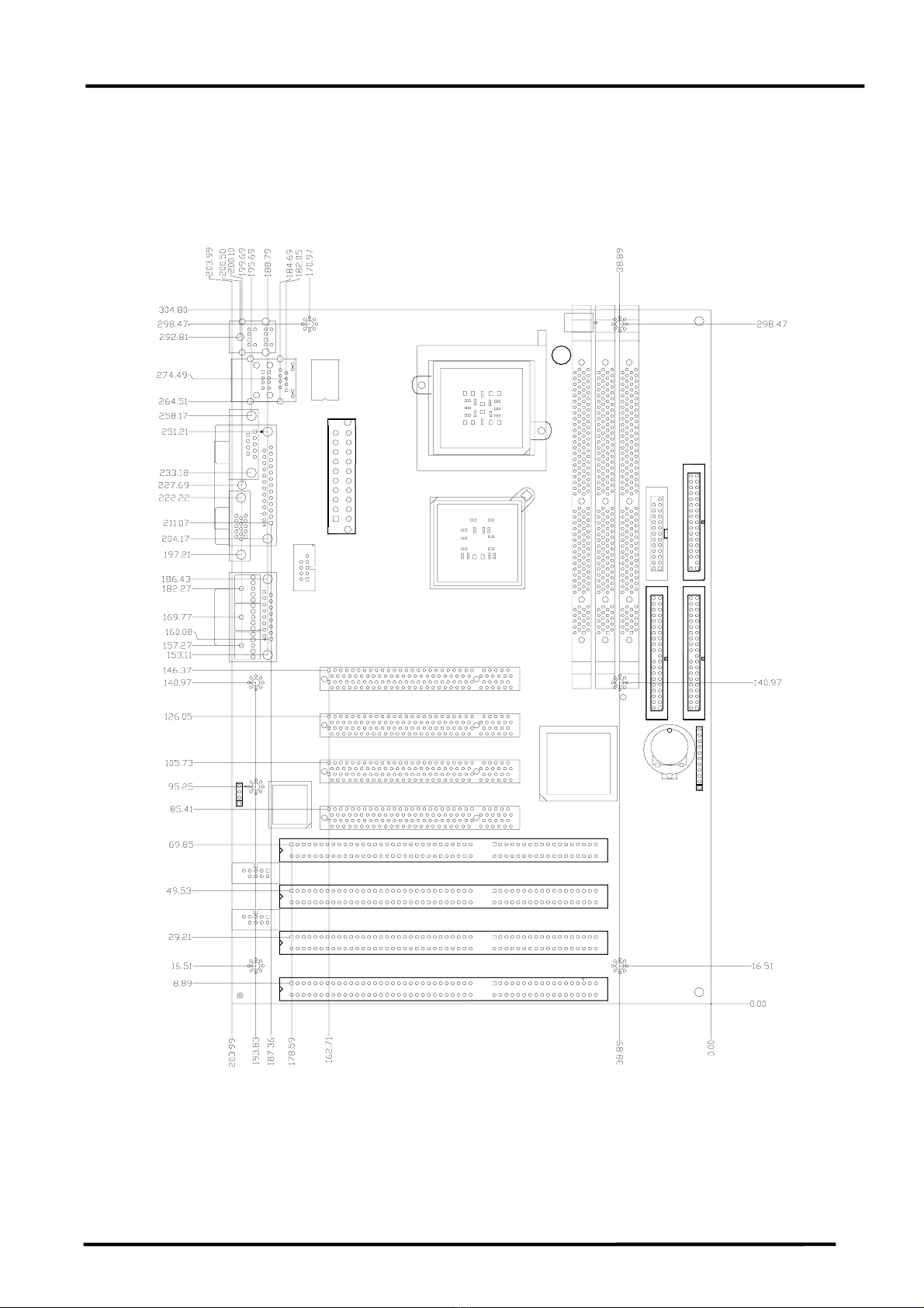
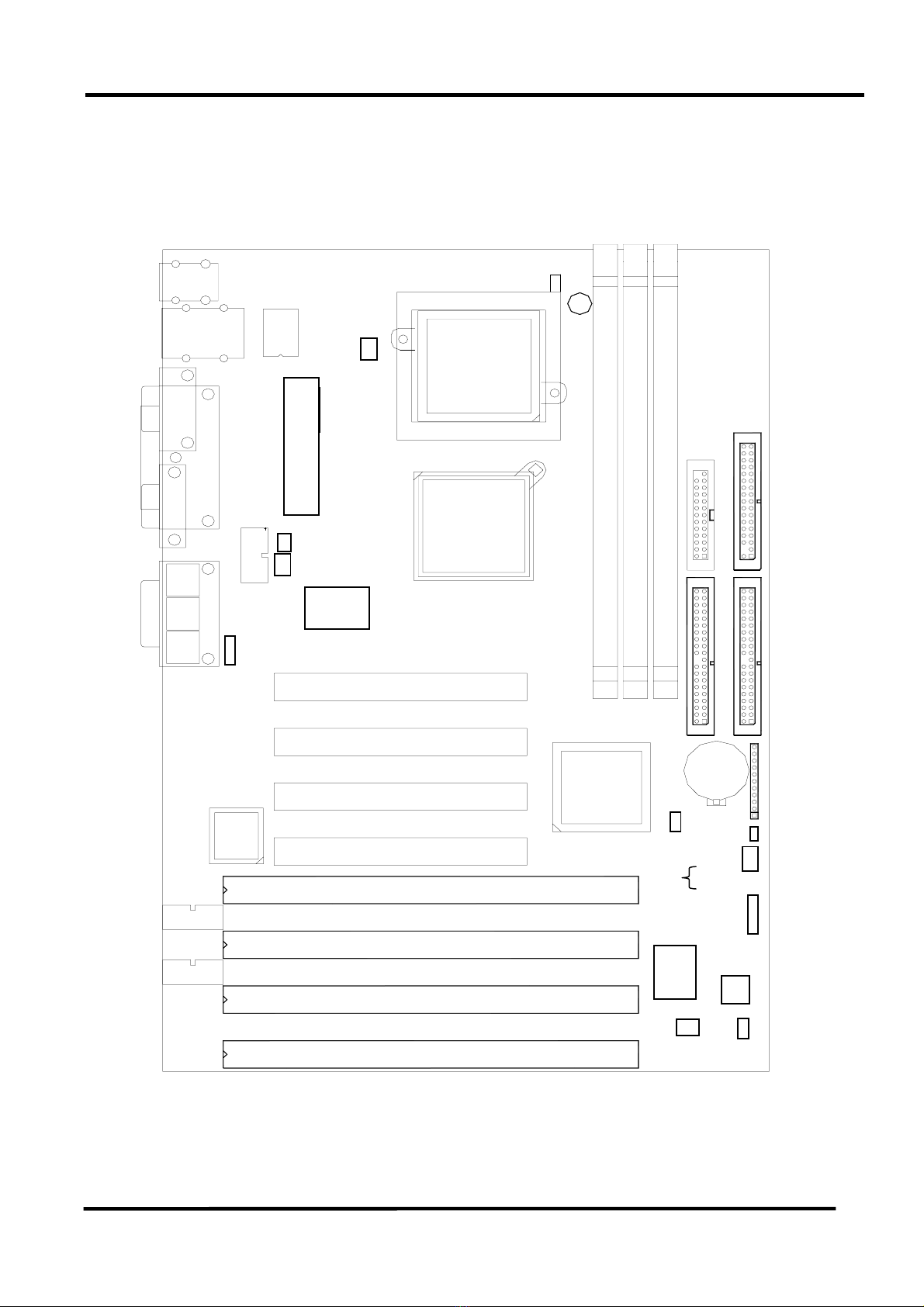
1.5 BOARD LAY O UT .........................................................................................................................................................4
CHAPTER 2 INSTALLATION .......................................................................................................................................5
2.1 SYSTEM MEMORY INSTALLATION ..............................................................................................................................5
2.2 JUMPER SETTINGS AND CONNECTORS........................................................................................................................6
2.2.1 Board Outline.....................................................................................................................................................6
2.2.2 Jumper Settings Summary ..................................................................................................................................7
2.2.3 I/O Connectors Summary ...................................................................................................................................8
CHAPTER 3 BIOS SETUP............................................................................................................................................21
3.1 RUNNING AWARD BIOS ........................................................................................................................................21
3.2 CMOS SETUP UTILITY ............................................................................................................................................22
3.3 STAND ARD CMOS SETUP ........................................................................................................................................24
3.4 BIOS FEATURES SETUP............................................................................................................................................27
3.5 CHIPSET FEATURES SETUP .......................................................................................................................................29
3.6 INTEGRATED PERIPHERALS ......................................................................................................................................32
3.7 POWER MANAGEMENT SETUP..................................................................................................................................36
3.8 PNP/PCI CONFIGURATION .......................................................................................................................................38
3.9 PC HEALTH STATUS (OPTIONAL) .............................................................................................................................40
3.10 LOAD OPTIMIZED DEFAULTS..................................................................................................................................41
3.11 SET SUPERVISOR / USER PASSWORD ......................................................................................................................42
3.12 SAV E & EXIT SETUP...............................................................................................................................................43
3.13 EXIT WITHOUT SAV I N G ..........................................................................................................................................44
CHAPTER 4 DRIVERS SUPPORT..............................................................................................................................45
4.1 USE YOUR DRIVER CD-ROM..................................................................................................................................45
4.2 FILE DIRECTORY ......................................................................................................................................................45
APPENDIX A. WATCH-DOG TIMER.........................................................................................................................46
RMA SERVICE REQUEST FORM .............................................................................................................................48


Chapter1 Introduction
1
User’s Manual
Chapter 1 Introduction
1.1 Introduction
IMB-X60 With its rich AGP 4X integrated graphics capabilities, flexible FSB settings, and support for
PC133 DRAM, the IMB-X60 delivers excellent levels of scalability and performance on a cost-effective,
High integrated platform designed for the specific needs of the ,Automation ,POS,Information PC, and
Internet Appliance market segments.
Intel ULV 400MHz + VIA Apollo PLE133 - Ultimate Value Combination
IMB-X60 optimizes the performance of the Intel Ultra Low Voltage Processor while its integrated AGP 4X
graphics engine delivers rich graphics capabilities for running 2D/3D software and Internet applications.
Its highly scaleable asynchronous bus design also makes it the ideal solution for Intel Celeron™
processors running at 100/133MHz FSB speeds. With an advanced memory controller architecture, the
IMB-X60 supports up to 1.5GB of high-speed PC133 SDRAM . These advanced memory technologies
provide the bandwidth and performance necessary for even the most demanding Internet and 3D
graphics applications. Further integrated CPU & multimedia & connectivity features that help minimize
the cost of building automation and Internet Appliances without sacrificing features and performance
include an integrated 10/100 BaseT Ethernet controller, AC-97 audio, MC-97 modem, Super I/O,
hardware monitoring capabilities, plus support for four USB ports, ATA 100, and advanced power
management.
1.2 Features
z Intel uFCBGA 400MHz CPU on Board
z VIA VT8601A North Bridge and VT82C686B South Bridge
z Award BIOS
z Integrated AGP 4X Graphics Engine
z AC 97 Audio
z Realtek RTL 8100C 10/100M Ethernet
z 4 x PCI and 4 x ISA expansion slots (Either one PCI or one ISA is shared )
z 1 x LAN, 1 x FDD, 4 x COM, 2 x LPT, Keyboard & Mouse, 4 x USB, 1 x IrDA and 1 x VGA
z Watchdog Timer
z ATX Power Connector

Chapter 1 Introduction
2 User’s Manual
1.3 Specification
IMB-X60 Series
CPU INTEL uFCBGA ULV 400MHz
L2 Cache 256K
Chipset 8601A+686B
FSB 100 MHz
Processor System
BIOS Award, 2 Mbit(Max)
Technology 3 X SDR/PC133
Max. Capacity 1.5GB
Memory
Socket DIMM
Controller 1 x Realtek 8100C
Interface 10/100 Base-T interface
Ethernet
Connector One RJ-45 connectors
Mode PCI IDE ATA33/66/100
EIDE
Channel 2
VGA 1 X DB-15
Serial port 1 x DB-9; 3x( 2x5 con.)
Parallel port 1 x DB-25; 1x Connector
USB 4 x USB 1.1 (2 in.,2 ext.)
I/O Interface
Audio AC’97
Game port 1 X DB15
Flash Memory Disk Support DOM
Expansion Bus 4 X PCI and 4 ISA (Either one PCI or one ISA is shared)
Health Monitoring Integrated in 686B
RTC Internal RTC with Li battery
Watchdog Timer 16 Lever time-out intervals
Power Connector ATX
Operating 0°C ~ 60°C
Temperature
Storage -20°C ~ 70°C
Humidity 5% ~ 95% RH, non-condensing
Net weight TBC
EMI/EMS FCC/CE Compliance
Dimensions 30.5 x 20 cm
Power Supply ±5V, ±12V,+3.3V
IMB-X60A Intel ULV Celeron 400MHz; 4S/2P; 2Ch. Audio;10/100M LAN
Model Extension
IMB-X60C Intel ULV Celeron 400MHz; 2S/1P

Chapter1 Introduction
3
User’s Manual
1.4 Unpack your IMB-X60 Series
Before you begin to install your card, please make sure that you received the following materials as listed
below:
Standard Packing:
z IMB-X60 x 1 pc Industrial Motherboard Computer
z Driver Utility CD-ROM x 1 pc Drivers & Utilities
z User's Manual x 1 pc This User's Manual
z IDE cable x 1 pc ATA100 40P IDE 80 Impendence P20 with Key
z FDD cable x 1 pc FDC. Cable 34 to 34Pin P4 with Key
z USB Y cable x 1 pc (only IMB-X60A) 2 x 5P W/Bracket P3, P8 with Key 50cm
z Com port cable x 1 pc (only IMB-X60A) Comport x 2 Cable & Bracket Two 2 x5 K10 50cm
z COM+LPT cable x 1 pc (only IMB-X60A) COM+LPT cable & BKT, D-SUB 9+D-SUB25 with Key 50cm

Chapter 1 Introduction
4 User’s Manual
1.5 Board Layout

Chapter 2 Installation
5
User’s Manual
Chapter 2 Installation
2.1 System Memory Installation
Step1: Open latches of DIMM socket.
Step2: Insert the RAM module into the DIMM socket.
Step3: Press the latches into the notches of the RAM module.

Chapter 2 Installation
6 User’s Manual
2.2 Jumper Settings and Connectors
2.2.1 Board Outline
*Full-size PCI Card can’t be inserted in PCIA1.
KM1
T
: Mouse
B: Keyboard
USBLN1
T
: LAN
M: USB2
B : USB1
Parallel Port
COMA1 VGAA1
Line-out
Line-in
Mic-in
Game Port
Transform
HN24012S
FAN1
ATX Power Connector
PSA1
Intel ULV
400MHz
SC2T1
SC2T2
COMB1
North Bridge
VT8601A
Realtek
8100C
PCIA1
COMB2
PCIA2
PCIA3
PCIA4
ISA4
ISA3
ISA2
CDIN1
ISA1
BIOS CMOS1
South Bridge
V
T82C686B
WOL1
FAN2
USBF1
USB3
USB4
PSW1
IRDA1
COMB3
W83877TF
CR2032
3V
PLRS1
DIMMA2
DIMMA3
DIMMA1
IDEB2
LPTA1
IDEB1
FDCA1 Wdg
isp2032e
LPTB1
GMSUN1

Chapter 2 Installation
7
User’s Manual
2.2.2 Jumper Settings Summary
LOCATION FUNCTION
CMOS1 Clear CMOS Data
SC2T1/SC2T2 Select COM2 Type
z CMOS1 : Clear CMOS Data
Description CMOS1
Normal (Default) 1-2
Clear CMOS 2-3
zSC2T1/SC2T2:Select COM2 Type
COM2 TYPE SC2T1 SC2T2
RS-232 (Factory) 1-2 1-5,2-6,3-7,4-8
RS-422 3-4 5-9,6-10,7-11,8-12
RS-485 5-6 5-9,6-10,7-11,8-12
Clear CMOS1
Normal (Default)
CMOS1
3
2
1
CMOS1
3
2
1
3
2
1
RS-422
RS-485
RS-232
SC2T1
6
4
2
4
3
2
1
SC2T2
12
11
10
9
5
3
1
CMOS1
Default : 12
11
10
9
4
3
2
1
SC2T2
SC2T1
6
4
2
5
3
1
SC2T1
SC2T2

Chapter 2 Installation
8 User’s Manual
2.2.3 I/O Connectors Summary
zPSW1:For ATX Power Button
Pin No. Description
1 PWRSW
2 GND
LOCATION FUNCTION
PSW1 For ATX Power Button
PLRS1 Power LED, HD, LED, Reset, Speaker Connector (11 Pin 2.54mm)
FAN1 3 Pin FAN Connector (CPU FAN)
FAN2 3 Pin FAN Connector (SYSTEM FAN)
WOL1 Walk On LAN Wafer 1°3
IDEB1 IDE Interface Connector (40 Pin 2.54mm Pitch Header)
IDEB2 IDE Interface Connector (40 Pin 2.54mm Pitch Header)
IRDA IRDA Connector
FDCA1 Floppy Interface Connector (34 Pin Header)
CDIN1 CD_IN Connector (2.54mm Pitch 180)
LPTB1 Parallel Port Connector (25 Pin D-Sub)
PSA1 20 Pin ATX Power Connector
KM1 Keyboard & Mouse Connector, Double stack 6 Pin mini DIN Female
COMA1 RS-232 Serial Port #1 Connector (D-Sub)
VGAA1 VGA Connector (15 Pin D-Sub)
COMB1 Serial Port #2 Connector (Header)
COMB2 Serial Port #3 Connector (Header)
COMB3 Serial Port #4 Connector (Header)
GMSUN1 Game Port & Sound Connector
USBLN1 USB Port #1, Port #2 & LAN Port (Top: LAN, Bottom: USB)
USBF1 USB Port #3 & #4 Connector 2°4 Pin 2.54mm
SPOT1 Digital Output Connector 1°4 Header 2.54mm (Optional)
SPIN1 Digital Input Connector 1°2 Header 2.54mm (Optional)
SOUNC1 6 Channel Sound Connector 2°5 Header 2.54mm (Optional)
PSW1 2
1
PSW1

Chapter 2 Installation
9
User’s Manual
zPLRS1: Power LED, HD LED, Reset, Speaker Connector (11 Pin 2.54mm)
Pin No. Description
1 Power LED +
2 Power LED +
3 GND
4 HDD LED +
5 HDD LED -
6 RESET SW +
7 RESET SW – (GND)
8 External Speaker -
9 Internal Buzzer -
10 NC
11 External Speaker +
zFAN1 : 3 Pin FAN Connector (CPU FAN)
Pin No. Description
1 Ground
2 +12V
3 FAN Status
Default: OFF
Default : 8-9 (ON) Internal Buzzer
1
11
PLRS1
FAN1
1
2
3
PLRS1
FAN1

Chapter 2 Installation
10 User’s Manual
zFAN2 : 3 Pin FAN Connector (SYSTEM FAN)
Pin No. Description
1 Ground
2 +12V
3 FAN Status
zWOL1:
::
:Walk On LAN Wafer1x3
Pin No. Description
1 WAKEUP
2 GND
3 5VSB
FAN2
3 2 1
FAN2
WOL1

Chapter 2 Installation
11
User’s Manual
zIDEB1 : IDE Interface Connector ( 40 Pin 2.54mm Pitch Header )
Pin No. Description Pin No. Description
1 Reset # 2 Ground
3 Data 7 4 Data 8
5 Data 6 6 Data 9
7 Data 5 8 Data 10
9 Data 4 10 Data 11
11 Data 3 12 Data 12
13 Data 2 14 Data 13
15 Data 1 16 Data 14
17 Data 0 18 Data 15
19 Ground 20 KEY
21 DMA REQ# 22 Ground
23 IOW # 24 Ground
25 IOR # 26 Ground
27 IOCHRDY 28 Ground
29 DMA ACK # 30 Ground
31 Interrupt 32 NC
33 SA1 34 PD80P / SD80P
35 SA0 36 SA2
37 HDC CS0 # 38 HDC CS1 #
39 HDD Active LED # 40 Ground
IDEB1
2 1
40 39
IDEB1

Chapter 2 Installation
12 User’s Manual
zIDEB2 : IDE Interface Connector (40 Pin 2.54mm Pitch Header)
Pin No. Description Pin No. Description
1 Reset # 2 Ground
3 Data 7 4 Data 8
5 Data 6 6 Data 9
7 Data 5 8 Data 10
9 Data 4 10 Data 11
11 Data 3 12 Data 12
13 Data 2 14 Data 13
15 Data 1 16 Data 14
17 Data 0 18 Data 15
19 Ground 20 KEY
21 DMA REQ# 22 Ground
23 IOW # 24 Ground
25 IOR # 26 Ground
27 IOCHRDY 28 Ground
29 DMA ACK # 30 Ground
31 Interrupt 32 NC
33 SA1 34 PD80P / SD80P
35 SA0 36 SA2
37 HDC CS0 # 38 HDC CS1 #
39 HDD Active LED # 40 Ground
IDEB2
2 1
40 39
IDEB2

Chapter 2 Installation
13
User’s Manual
zIRDA1: IRDA Connector
Pin No. Description
1 VCC
2 NC
3 IRRX
4 GND
5 IRTX
zFDCA1: Floppy Interface Connector (34 Pin Header)
Pin No. Description Pin No. Description
1 Ground 2 Density Select
3 Ground 4 KEY
5 Ground 6 DS1
7 Ground 8 Index #
9 Ground 10 Motor Enable A #
11 Ground 12 Drive Select B #
13 Ground 14 Drive Select A #
15 Ground 16 Motor Enable B #
17 Ground 18 Direction #
19 Ground 20 Step #
21 Ground 22 Write Data #
23 Ground 24 Write Gate #
25 Ground 26 Track 0 #
27 Ground 28 Write Protect #
29 NC 30 Read Data #
31 Ground 32 Head Side Select #
33 NC 34 Disk Change #
IRDA1
5
1
FDCA1
2 1
34 33
IRDA1
FDCA1

Chapter 2 Installation
14 User’s Manual
zCDIN1:
::
:CD_IN Connector(
((
(2.54mm Pitch 180°
°°°)
))
)
Pin No. Description
1 CDL
2 CO_GND
3 CO_GND
4 CDR
zLPTB1:
::
:Parallel Port Connector (25 Pin D-Sub)
Pin No. Description Pin No. Description
1 Strobe # 14 Auto Form Feed #
2 Data 0 15 Error #
3 Data 1 16 Initialize #
4 Data 2 17 Printer Select IN #
5 Data 3 18 Ground
6 Data 4 19 Ground
7 Data 5 20 Ground
8 Data 6 21 Ground
9 Data 7 22 Ground
10 Acknowledge # 23 Ground
11 Busy 24 Ground
12 Paper Empty 25 Ground
13 Printer Select
CDIN1
4
1
1
13
14
25
LPTB1
CDIN1
LPTB1

Chapter 2 Installation
15
User’s Manual
zPSA1: 20 Pin ATX Power Connector
Pin No. Description Pin No. Description
1 +3.3V 11 +3.3V
2 +3.3V 12 -12V
3 GND 13 GND
4 +5V 14 PS-ON
5 GND 15 GND
6 +5V 16 GND
7 GND 17 GND
8 Power Good 18 -5V
9 Stand-By 5V 19 +5V
10 +12V 20 +5V
zKM1:
::
:Keyboard & Mouse Connector
Double stack 6 Pin mini DIN Female
Pin No. Description
1 KBDATA
2 NC
3 GND
4 +5V
5 KBCLK
6 NC
7 MSDATA
8 NC
9 GND
10 +5V
11 MSCLK
12 NC
PSA1
20
11
10
1
PSA1
KM1

Chapter 2 Installation
16 User’s Manual
zCOMA1: RS-232 Serial Port #1 Connector (D-Sub)
Description
Pin No. RS-232
1 Data Carrier Detect (DCD1 #)
2 Data Set Ready (DSR1 #)
3 Receive Data (RXD1)
4 Request To Send (RTS1 #)
5 Transmit Data (TXD1)
6 Clear To Send (CTS1 #)
7 Data Terminal Ready (DTR1 #)
8 Type Select1
9 Ground
z
zz
zVGAA1 : External VGA Connector ( 15 Pin D-Sub )
Pin No. Description
1 Red Color Signal
2 Green Color Signal
3 Blue Color Signal
4 NC
5 Ground
6 Ground
7 Ground
8 Ground
9 NC
10 Ground
11 NC
12 DDC-DATA
13 H-Sync.
14 V-Sync.
15 DDC-CLK
COMA1
1
6
5
9
COMA1
COMA1
VGAA1
5 1
610
1115
Table of contents
Other Lanner electronics Motherboard manuals
Popular Motherboard manuals by other brands

NXP Semiconductors
NXP Semiconductors QorIQ FRDM-LS1012A Reference manual

Asus
Asus F1A55-M LX PLUS R2.0 quick start guide

MSI
MSI X299 TOMAHAWK ARCTIC quick start

National Semiconductor
National Semiconductor ADC14DC105 user guide

Cypress Semiconductor
Cypress Semiconductor CapSense CY8CKIT-024 Guide

Team Orion
Team Orion Vortex DSB-R+ instruction manual

Silicon Laboratories
Silicon Laboratories Si80xx-EVB user guide

Nvidia
Nvidia nForce 680I LT SLI user manual

Gigabyte
Gigabyte GA-H81M-S2VP user manual

Congatec
Congatec COM Express conga-TR3 user guide

Texas Instruments
Texas Instruments J721E user guide

EPH Controls
EPH Controls R27-RF operating instructions