ST SPC563M64CAL144 User manual

September 2013 Doc ID 024080 Rev 3 1/38
RM0345
Reference manual
SPC563M64CAL144
calibration adapter board for SPC563M64xx devices
Introduction
The SPC563M64CAL144 (rev.B) system is designed to enable the use of new enhanced
automotive calibration and debug tools on the SPC563M64xx family of automotive
microcontrollers.
The SPC563M64CAL144 (rev.B) can be fitted onto the application printed circuit board
(PCB) in place of the standard SPC563M64xx family microcontroller in LQFP144 package.
SPC563M64CAL144 (rev.B) hardware is designed to support two standardized tool
connectors, allowing a variety of calibration and debug hardware to be connected and
reused
Figure 1. SPC563M64CAL144 (rev.B)
Table 1. Board summary
Order code On board device Target footprint
SPC563M64CAL144 SPC563M64xx QFP144
*$3*5,
www.st.com

Contents RM0345
2/38 Doc ID 024080 Rev 3
Contents
1 Calibration system overview . . . . . . . . . . . . . . . . . . . . . . . . . . . . . . . . . . 6
1.1 Features overview . . . . . . . . . . . . . . . . . . . . . . . . . . . . . . . . . . . . . . . . . . . 6
2 Power supply . . . . . . . . . . . . . . . . . . . . . . . . . . . . . . . . . . . . . . . . . . . . . . . 7
3 Reset and configuration signals . . . . . . . . . . . . . . . . . . . . . . . . . . . . . . 11
4 Calibration bus interface and External Memory . . . . . . . . . . . . . . . . . . 12
4.1 External memory specification . . . . . . . . . . . . . . . . . . . . . . . . . . . . . . . . . 12
4.2 SRAM supply and data retention function . . . . . . . . . . . . . . . . . . . . . . . . 12
4.3 Calibration bus interface . . . . . . . . . . . . . . . . . . . . . . . . . . . . . . . . . . . . . . 14
5 Development connector . . . . . . . . . . . . . . . . . . . . . . . . . . . . . . . . . . . . . 15
6 Calibration connector . . . . . . . . . . . . . . . . . . . . . . . . . . . . . . . . . . . . . . . 17
7 Tool IO . . . . . . . . . . . . . . . . . . . . . . . . . . . . . . . . . . . . . . . . . . . . . . . . . . . 19
8 CAN interface . . . . . . . . . . . . . . . . . . . . . . . . . . . . . . . . . . . . . . . . . . . . . . 20
9 Calibration software compatibility and configuration . . . . . . . . . . . . . 22
9.1 Calibration bus sw configuration . . . . . . . . . . . . . . . . . . . . . . . . . . . . . . . 22
9.1.1 Cal Bus PCR Settings . . . . . . . . . . . . . . . . . . . . . . . . . . . . . . . . . . . . . . 22
9.1.2 Cal Bus ECCR Settings . . . . . . . . . . . . . . . . . . . . . . . . . . . . . . . . . . . . . 23
9.1.3 Cal Bus EBI Settings . . . . . . . . . . . . . . . . . . . . . . . . . . . . . . . . . . . . . . . 24
9.2 Example Configuration CODE . . . . . . . . . . . . . . . . . . . . . . . . . . . . . . . . . 27
Appendix A Calibration base footprints . . . . . . . . . . . . . . . . . . . . . . . . . . . . . . . . 29
Appendix B Mechanical constrains . . . . . . . . . . . . . . . . . . . . . . . . . . . . . . . . . . . 30
Appendix C Schematic. . . . . . . . . . . . . . . . . . . . . . . . . . . . . . . . . . . . . . . . . . . . . . 33
Appendix D Options placement. . . . . . . . . . . . . . . . . . . . . . . . . . . . . . . . . . . . . . . 36

List of tables RM0345
4/38 Doc ID 024080 Rev 3
List of tables
Table 1. Board summary . . . . . . . . . . . . . . . . . . . . . . . . . . . . . . . . . . . . . . . . . . . . . . . . . . . . . . . . . . 1
Table 2. J15, J2 and J14 option cut traces. . . . . . . . . . . . . . . . . . . . . . . . . . . . . . . . . . . . . . . . . . . . 10
Table 3. Reset and configuration signals . . . . . . . . . . . . . . . . . . . . . . . . . . . . . . . . . . . . . . . . . . . . . 11
Table 4. J11 configuration of SRAM supply for retention mode . . . . . . . . . . . . . . . . . . . . . . . . . . . . 13
Table 5. J3, J5 and J10 option cut traces. . . . . . . . . . . . . . . . . . . . . . . . . . . . . . . . . . . . . . . . . . . . . 15
Table 6. Nexus signals on AMP 38 Mictor connector. . . . . . . . . . . . . . . . . . . . . . . . . . . . . . . . . . . . 16
Table 7. Nexus signals on AMP 38 Mictor connector. . . . . . . . . . . . . . . . . . . . . . . . . . . . . . . . . . . . 17
Table 8. J12, J13 FlexCAN interface selection. . . . . . . . . . . . . . . . . . . . . . . . . . . . . . . . . . . . . . . . . 20
Table 9. J6, J17 and J7 FlexCAN interface selection. . . . . . . . . . . . . . . . . . . . . . . . . . . . . . . . . . . . 21
Table 10. CAN transceiver operating voltage selection . . . . . . . . . . . . . . . . . . . . . . . . . . . . . . . . . . . 21
Table 11. Calibration bus signals configuration . . . . . . . . . . . . . . . . . . . . . . . . . . . . . . . . . . . . . . . . . 22
Table 12. EBDF field definition . . . . . . . . . . . . . . . . . . . . . . . . . . . . . . . . . . . . . . . . . . . . . . . . . . . . . . 23
Table 13. EBI_MCR register setting. . . . . . . . . . . . . . . . . . . . . . . . . . . . . . . . . . . . . . . . . . . . . . . . . . 24
Table 14. EBI_CAL_BRx register setting . . . . . . . . . . . . . . . . . . . . . . . . . . . . . . . . . . . . . . . . . . . . . . 25
Table 15. EBI_CAL_BOx register setting . . . . . . . . . . . . . . . . . . . . . . . . . . . . . . . . . . . . . . . . . . . . . . 26
Table 16. Document revision history . . . . . . . . . . . . . . . . . . . . . . . . . . . . . . . . . . . . . . . . . . . . . . . . . 37

RM0345 List of figures
Doc ID 024080 Rev 3 5/38
List of figures
Figure 1. SPC563M64CAL144 (rev.B). . . . . . . . . . . . . . . . . . . . . . . . . . . . . . . . . . . . . . . . . . . . . . . . . 1
Figure 2. Power supply . . . . . . . . . . . . . . . . . . . . . . . . . . . . . . . . . . . . . . . . . . . . . . . . . . . . . . . . . . . . 7
Figure 3. Supply signals from the QFP144 footprint . . . . . . . . . . . . . . . . . . . . . . . . . . . . . . . . . . . . . . 8
Figure 4. Test points on J4 connector . . . . . . . . . . . . . . . . . . . . . . . . . . . . . . . . . . . . . . . . . . . . . . . . . 8
Figure 5. Supply signals on SPC563M64xx CSP496 . . . . . . . . . . . . . . . . . . . . . . . . . . . . . . . . . . . . . 9
Figure 6. SRAM supply circuitry. . . . . . . . . . . . . . . . . . . . . . . . . . . . . . . . . . . . . . . . . . . . . . . . . . . . . 13
Figure 7. SRAM schematic diagram . . . . . . . . . . . . . . . . . . . . . . . . . . . . . . . . . . . . . . . . . . . . . . . . . 14
Figure 8. JP1 development connector . . . . . . . . . . . . . . . . . . . . . . . . . . . . . . . . . . . . . . . . . . . . . . . . 15
Figure 9. AMP 38 Mictor . . . . . . . . . . . . . . . . . . . . . . . . . . . . . . . . . . . . . . . . . . . . . . . . . . . . . . . . . . 16
Figure 10. J9 Calibration connector. . . . . . . . . . . . . . . . . . . . . . . . . . . . . . . . . . . . . . . . . . . . . . . . . . . 17
Figure 11. Calibration triggers TOOL_IO. . . . . . . . . . . . . . . . . . . . . . . . . . . . . . . . . . . . . . . . . . . . . . . 19
Figure 12. CAN schematic diagram. . . . . . . . . . . . . . . . . . . . . . . . . . . . . . . . . . . . . . . . . . . . . . . . . . . 20
Figure 13. TQPACK144SD . . . . . . . . . . . . . . . . . . . . . . . . . . . . . . . . . . . . . . . . . . . . . . . . . . . . . . . . . 29
Figure 14. Top and side view drawing . . . . . . . . . . . . . . . . . . . . . . . . . . . . . . . . . . . . . . . . . . . . . . . . . 30
Figure 15. Side and bottom view drawing . . . . . . . . . . . . . . . . . . . . . . . . . . . . . . . . . . . . . . . . . . . . . . 31
Figure 16. Complete system side view drawing. . . . . . . . . . . . . . . . . . . . . . . . . . . . . . . . . . . . . . . . . . 32
Figure 17. SPC563M64xx in CSP package schematic . . . . . . . . . . . . . . . . . . . . . . . . . . . . . . . . . . . . 33
Figure 18. Polypod-TQ144 connector schematic. . . . . . . . . . . . . . . . . . . . . . . . . . . . . . . . . . . . . . . . . 34
Figure 19. Memory, CAN and connectors schematic . . . . . . . . . . . . . . . . . . . . . . . . . . . . . . . . . . . . . 35
Figure 20. Options placement . . . . . . . . . . . . . . . . . . . . . . . . . . . . . . . . . . . . . . . . . . . . . . . . . . . . . . . 36

Calibration system overview RM0345
6/38 Doc ID 024080 Rev 3
1 Calibration system overview
The Calibration Adapter board features 2 Mbytes of SRAM in order to substitute to the
SPC563M64xx internal Flash during calibration.
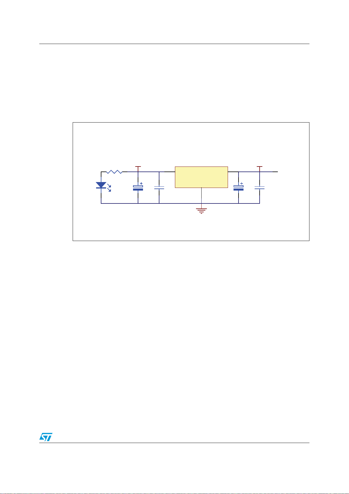
A voltage regulator is also integrated upon the board to generate, from selectable 5 V
source, the 3.3 V voltage for the RAM and the calibration bus interface.
Development connector (Mictor AMP38) is providing the interface for the debug and trace
tools.
A calibration connector (ERNI 154819) is providing an interface optimized for calibration
usage.
A high speed CAN transceiver is connected to the FlexCAN of the mcu device.
The components chosen in the design of this board are automotive qualified to allow system
evaluation over the full automotive evaluation range (-40 °C to 125 °C).
1.1 Features overview
calibration systems include these distinctive features:
●
Use 100% production silicon, ensuring full hardware and software compatibility
between production and calibration systems;
●
Support LQFP144 MCU production package allowing calibration systems to be built
without requiring modifications to the standard production system housing;
●
2MByte static RAM organized as 1024K words by 16 bits;
●
On-board latch providing a 16-bit de-multiplexed bus interface from the SPC563M64xx
16-bit multiplexed calibration interface;
●
Support for Nexus-based debug tools even if application PCB does not include Nexus
connector;
●
Nexus functionality with 12 Message Data Out (MDO) signals;
●
Support for full-feature calibration tools, via availability of comprehensive set of device
signals available on the connectors;
●
ERNI 154819 connector optimized for calibration;
●
High speed CAN transceiver with signals protection;
●
Allows system calibration without impacting standard MCU I/O resources;
●
Allows system calibration regardless of availability of standard MCU external bus;
●
Uses tried and tested technology.

RM0345 Power supply
Doc ID 024080 Rev 3 7/38
2 Power supply
The Calibration boards requires a +5 V to supply the on board CAN transceiver and a
+3.3 V to supply the SPC563M64xx calibration bus interface and for the external RAM.
The 3.3 V supply is generated on the SPC563M64CAL144 (rev.B) via the very low drop
voltage regulator by using the +5V. A LED (D1) will light when the board is powered.
Figure 2. Power supply
By default the 5V is taken from the target application through the VDDREG supply level
(supply input for the internal voltage regulators of the SPC563M64xx). Gauge J14 enables
the powering from the application board. Table 2 shows its option configuration.
In case that no additional power loading could be applied to the application system during
calibration, the +5V can be supplied externally via J4 connector (+5V test point, see
Figure 4) and the gauge J14 (see Figure 3) must be open.
9 9
5
&
Q
&
X)
&
Q
&
X)
*1 '
,1
*1'
287
8 /)&'775<
*$3*5,

Power supply RM0345
8/38 Doc ID 024080 Rev 3
Figure 3. Supply signals from the QFP144 footprint
Figure 4. Test points on J4 connector
All power signals and voltage references of the SPC563M64xx QFP144 footprint from the
application board are directly connected to the respective calibration device signals.
The VDDE12 supply used to power the dedicated SPC563M64xx calibration bus interface is
connected to the upon board +3.3 V voltage regulator.
VSSAVSSSYN
GND
VRCCTL
VDDREG
VSTBY
C46
1uF
GND
VDDEH1.A 24
VDDEH1B 34
VDDEH1C 46
VDDEH4 61
VDDEH6A 78
VDDEH6B 93
VDDEH7 102
VDDEH7 113
VDDPLL 74
VDDREG 10
VRC33 13
VRCCTL 11
VSSPLL 77
VSSA0 7
VSTBY 12
VDDA0 6
VSUP 79 VDDA0
VDDSYN
Default = C
L
J15
J14
Default = CLOSE
+5V
VDDE H1B
VDDE H6A
VDDEH7
VDDEH6A
VDDEH1A
VDDEH1B
VDDEH6B
QFP144 footprint
GAPGRI00341
*1'
-
&21
9
9
9''
*$3*5,

RM0345 Power supply
Doc ID 024080 Rev 3 9/38
Figure 5. Supply signals on SPC563M64xx CSP496
The VRC33 signal of the CSP496 is connected to its respective signal of the QFP144 target
application via the J15 cut trace option.
The VRC33 can be also connected to the on board +3.3V by closing the J2 gauge. In this
case the gauge J15 must be open (Table 2).
&B5'B:5
&B:(
&B:(
&B2(
&B76
&B0&.2
&B(972
9
9
-
95&
&YUFSOBM#VT*OUFSGBDF&#*
&B$'' 0
&B$'' 0
&B$'' 9
&B$'' /
&B$'' 7
&B$'' .
&B$'' /
&B$'' 8
&B$'' 9
&B$'' $%
&B$'' $%
&B'$7 :
&B'$7 <
&B'$7 9
&B'$7 :
&B'$7 8
&B'$7 8
&B'$7 7
&B'$7 7
&B'$7 $$
&B'$7 $%
&B'$7 $$
&B'$7 $%
&B'$7 $$
&B'$7 $%
&B'$7 $$
&B'$7 $%
&B5'B:5 :
&B:( <
&B:( $$
&B2( $'
9''( $$
9''( $$
9''( $%
9''( $%
9''( $(
9''( $*
9''( $*
9''( .
9''( 1
9''( 5
9''( 5
9''( 5
9''( 5
9''( 5
9''( 5
9''( 7
9''( 7
9''( 7
9''( 7
9''( 8
9''( 8
9''( 8
9''( 8
9''( 9
9''( 9
9''( 9
9''( 9
9''(+ -
9''(+ *
9''(+ $'
9''(+$ 9
95& :
95& $(
95& %
95& '
9''(+% .
95& $)
9''(+ &
9''(+ '
9''(+ +
9''(+ -
9''(+ /
9''(+ /
9''(+ /
9''(+ /
9''(+ 0
9''(+ 1
9''(+ 3
9''(+ )
&B(972 *
&B0&.2 +
&B76 $$
8
63&0
$''5
$''5
$''5
$''5
$''5
$''5
$''5
$''5
$''5
$''5
$''5
'$7$
'$7$
'$7$
'$7$
'$7$
'$7$
'$7$
'$7$
'$7$
'$7$
'$7$
'$7$
'$7$
'$7$
'$7$
'$7$
9''(+
2SHQ[&87
&ORVH[&87
-
$
%
$
%
1&
9''(+$
9''(+$
9''(+%
9''(+%
9''(+%
*$3*5,

Power supply RM0345
10/38 Doc ID 024080 Rev 3
Table 2. J15, J2 and J14 option cut traces
(1)
1. Refer to Chapter Appendix D: Options placement for layout Jumper placement
Option
name Function Value Note
J15 VRC33 open VRC33 signal is disconnected from the target
application board
close
(default) VRC33 signal is connected to the target
application board
J2 VRC33
open
(default) VRC33 signal is disconnected from the on board
+3.3V signal
close VRC33 signal is connected to the
on board
+3.3V signal
J14 +5V supply open +5V is powered from J4 connector
close
(default) +5V is powered from target application via
VDDREG pin of the QFP144 target footprint

RM0345 Reset and configuration signals
Doc ID 024080 Rev 3 11/38
3 Reset and configuration signals
Calibration and debug tools may use the reset signals included in the connectors to have
visibility of when the SPC563M64xx device has been reset. Debug tools may also require
the ability to force device reset.
All signals of the SPC563M64xx QFP144 footprint from the application board are directly
connected to the respective calibration device signals. This includes the following signals on
the Table 3.
Table 3. Reset and configuration signals
Signal name Function Notes
Reset / Configuration (5)
/RESET External reset input
The /RESET pin is an active low input. The
RESET pin is asserted by an external device
during a power-on or external reset. The
internal reset signal asserts only if the RESET
pin asserts for 10 clock cycles. Assertion of
the RESET pin while the device is in reset
causes the reset cycle to start over.
/RSTOUT External reset output
The RSTOUT pin is an active low output that
uses a push/pull configuration. The RSTOUT
pin is driven to the low state by the MCU for all
internal and external reset sources. There is a
delay between initiation of the reset and the
assertion of the RSTOUT pin.
BOOTCFG[1] Boot configuration input
The BOOTCFG field holds the value of the
BOOTCFG[1] pin that was latched on the last
negation of the RSTOUT pin. The BOOTCFG
field is used by the BAM program to
determine the location of the Reset
Configuration Word.
PLLREF FMPLL Mode Selection
PLLREF is used to select whether the
oscillator operates in xtal mode or external
reference mode from reset.
If RSTCFG is 0, External reference clock
selected.
If RSTCFG is 1, Xtal oscillator mode is
selected
WKPCFG Weak Pull Configuration
The signal on the WKPCFG pin determines
whether weak pullup or pull down devicesare
enabled after reset on the eTPU and eMIOS
pins.
0: Weak pulldown applied to eTPU and
eMIOS pins at reset
1: Weak pullup applied to eTPU and eMIOS
pins at reset.

Calibration bus interface and External Memory RM0345
12/38 Doc ID 024080 Rev 3
4 Calibration bus interface and External Memory
The SPC563M64xx features a 16-bit de-multiplexed calibration bus interface that is
connected to an external 2Mbyte SRAM thanks to an on board latch.
4.1 External memory specification
The calibration board provides a SRAM with the following characteristics:
– 2Mbyte static RAMs organized as 1024K words by 16 bits;
– 16-bit data width;
– Fully static operation: no clock or refresh required;
– 3.3V input supply;
– /CE power-down;
– High-speed access time (10ns);
– Full automotive temperature range;
– Lead-free.
When /CE is HIGH (deselected), the device assumes a standby mode at which the power
dissipation can be reduced down with CMOS input levels.
4.2 SRAM supply and data retention function
The circuitry in Figure 6 has been implemented on the calibration board to protect the
memory and to guarantee that the Working Page is valid after a power fail of the target
application by putting the SRAM in standby powered.
The 3.3 V supply of the SRAM (Vmem) is gated by the RESET and RSTOUT signals of the
SPC563M64xx.
The memory enable is driven via the SPC563M64xx chip select C_CS0 “and” the RESETs
signals combination.

RM0345 Calibration bus interface and External Memory
Doc ID 024080 Rev 3 13/38
Figure 6. SRAM supply circuitry
The jumper J11 (see Figure 6) allows to select the standby operation of the SRAM.
The standby voltage can be selected between:
●
SPC563M64xx Vstby pin: same standby voltage as the internal RAM;
●
the 3.3V generated on the calibration board;
●
ECU_Stby supplied by the calibration connector J9 (see Figure 10).
Table 4. J11 configuration of SRAM supply for retention mode
J11 SRAM standby supply source
all open ECU_Stby: standby voltage on J9 calibration connector
1-2 closed Upon the board +3.3V generated
2-3 closed VSTBY input pin of the
SPC563M64xx
from the target application
+5V +3.3V
R1
330
D1
LED
C35
100n
C34
4.7uF
C37
100n
C36
2.2uF
GND
IN
1
GND
2
OUT 3
U2 LF33CDT-TRY
VSTBY
+3.3V
C31
1uF
GND
/RESET
Vmem
GND
Vmem
GND
5
3
1
2
4
U7
74V1G00CTR
53
1
2
4
U8
74V1G32CTR
ECU_Vstby
/RSOUT
/CE_RAM
/CS0
Vmem
D2
20CJQ060
Q1
STT5PF20V
13
2J11
GAPGRI00344

Calibration bus interface and External Memory RM0345
14/38 Doc ID 024080 Rev 3
4.3 Calibration bus interface
The calibration bus is made up of address bus, data bus, and bus control signals, and is
used on the calibration board to access the upon board memory.
The calibration board supports a 16-bit de-mulitplexed calibration bus. This is derived from
the multiplexed bus on the SPC563M64xx, where the majority of address lines are derived
from the data lines (CAL_DATA on SPC563M64 device), by using an onboard external latch
controlled by the C_TS signal. The ALE functionality of this signal indicates to the external
latch when to capture the address signals
Figure 7. SRAM schematic diagram
The Section 9: Calibration software compatibility and configuration shows the necessary
software configuration of the SPC563M64xx calibration interface.
/DWFKB4
/DWFKB4
/DWFKB4
/DWFKB4
/DWFKB4
/DWFKB4
/DWFKB4
/DWFKB4
&B76
&B76
&
Q
&
X)
*1'
&
Q
&
X)
*1'
9PHP
*1'
$''5
$''5
$''5
/DWFKB4
/DWFKB4
/DWFKB4
/DWFKB4
/DWFKB4
/DWFKB4
/DWFKB4
/DWFKB4
/DWFKB4
/DWFKB4
/DWFKB4
/DWFKB4
/DWFKB4
/DWFKB4
/DWFKB4
$''5
&6
&(B5$0
&B5'B:5
&B:(
&B:(
&B2(
2(
/(
'
4
'
4
'
4
'
4
'
4
'
4
'
4
'
4
9&&
*1'
8$
61/9&'**5
2(
/(
'
4
'
4
'
4
'
4
'
4
'
4
'
4
'
4
9&&
*1'
8%
61/9&'**5
*1'
*1'
9PHP
9PHP
9PHP
&(B5$0
&(B5$0
9PHP
/DWFKB4
/DWFKB4
'$7$
'$7$
'$7$
'$7$
'$7$
'$7$
'$7$
'$7$
/DWFKB4
/DWFKB4
/DWFKB4
/DWFKB4
/DWFKB4
'$7$
'$7$
'$7$
'$7$
'$7$
'$7$
'$7$
'$7$
'$7$
'$7$
'$7$
'$7$
'$7$
'$7$
'$7$
'$7$
'$7$
'$7$
'$7$
'$7$
'$7$
'$7$
'$7$
$
$
$
$
$
$
$
%
$
%
$
&
$
&
$
'
$
+
$
+
$
+
$
+
$
*
$
*
$
)
$
)
,2 %
,2 &
,2 &
,2 '
,2 (
,2 )
,2 )
,2 *
,2 %
,2 &
,2 &
,2 '
,2 (
,2 )
,2 )
,2 *
*1'
'
*1'
( 9'' '
9'' (
&( %
:( *
/% $
8% %
2( $
$
(
$
'
1&
$
1&
+
1&
(
$
* $
+
8
,6:9%//
*$3*5,

RM0345 Development connector
Doc ID 024080 Rev 3 15/38
5 Development connector
The JTAG signals and Nexus functionality with 12 Message Data Out (MDO) signals are
available on the JP1 development connector (Nexus connector).
A hardware control bit in the SPC563M64xx Nexus port controller, is used to control whether
the added signals for full width trace port are routed to the MDO[4:11] signals, or the
CAL_MDO[4:11] signals. This control bit is set by the cut trace J1 (default close) on the
NEXUSCFG pin of the SPC563M64xx device, as on the calibration board the
CAL_MDO[4:11] signals are routed to the JP1 development connector.
Figure 8. JP1 development connector
The option cut trace J3, J5 and J10 are listed on Figure 5.
Table 5. J3, J5 and J10 option cut traces
option
name Function Value Note
J3 CLKOUT open CLKOUT signal is disconnected to the Nexus JP1
connector
close
(default) CLKOUT signal is connected to the Nexus JP1
connector
J5 VSTBY open VSTBY signal is disconnected to the Nexus JP1
connector
close
(default) VSTBY signal is connected to the Nexus JP1
connector
J10 BOOTCFG1 open BOOTCFG1 signal is disconnected to the Nexus
JP1 connector
close
(default) BOOTCFG1 signal is connected to the Nexus
JP1 connector
*1'
$''5
$''5
$''5
$''5
$''5
$''5
$''5
$''5
$''5
$''5
$''5
$''5
&/.28
7
9
9
*1'
&
X)
&B0&.2
&B(972
1(;86
-
-
-
569'
569'
569'
569'
9(1B,2
&/.287
9(1B,2
9(1B,2
567,1
(97,
7'2
975()
9(1B,2
5'<
7&.
0'2
706
0'2
7',
0'2
-&203
0'2
9(1B,2
0'2
567287
0'2
722/B,2
0'2
722/B,2
0'2
8%$77
(972
8%$77
0&.2
722/B,2
06(2
9$/75()
06(2
*1'
-3
'()$8/7 &/26(
'()$8/7 &/26(
'()$8/7 &/26(
$''5
$''5
-&203
706
7'2
7',
7&.
5(6(7
*3,2B9
*3,2B9
%227&)*
$''5
967%<
9''(+$
5 .
*1'
*$3*5,

Development connector RM0345
16/38 Doc ID 024080 Rev 3
Figure 6 shows the mapping of the development connector that provides Debug, Nexus
trace and calibration signals. The port connector is an AMP 38 pin Mictor style.
Figure 9. AMP 38 Mictor
*) signal is connected via cut trace option
Table 6. Nexus signals on AMP 38 Mictor connector
Pin Description Pin Descriptio
1 nc 2 nc
3 nc 4 nc
5 C_MDO9 6 CLKOUT*
7 BOOTCFG1* 8 C_MDO8
9 /RESET 10 C_EVTI
11 TDO 12 +3.3V
13 C_MDO10 14 RDY
15 TCK 16 C_MDO7
17 TMS 18 C_MDO6
19 TDI 20 C_MDO5
21 JCOMP 22 C_MDO4
23 C_MDO11 24 C_MDO3
25 nc 26 C_MDO2
27 10K pull down resistor 28 C_MDO1
29 TOOL_IO1 30 C_MDO0
31 VDDEH1A 32 C_EVTO
33 VDDEH1A 34 C_MCKO
35 TOOL_IO0 36 C_MSEO1
37 VSTBY* 38 C_MSEO0
SLQQ
*$3*5,

RM0345 Calibration connector
Doc ID 024080 Rev 3 17/38
6 Calibration connector
The board is equipped with an ERNI connector to give a more robust solution in terms of
physical connectivity for Calibration purpose.
Figure 10. J9 Calibration connector
The Table 7 shows the mapping of the calibration connector that provides Debug and
calibration signals. The port connector is an ERNI 154819 style.
Table 7. Nexus signals on AMP 38 Mictor connector
Pin SPC563M64xx
routing standard function Pin SPC563M64xx
routing standard function
B1 nc nc A1 nc nc
B2 nc nc A2 JCOMP JTAG interface
B3 /RSOUT /RSOUT A3 CAL Wakeup 12V output for Wakeup
functionality
B4 GND GND A4 C_EVTI JTAG interface
B5 GND GND A5 TDO JTAG interface
B6 GND GND A6 TMS JTAG interface
B7 GND GND A7 TCK JTAG interface
B8 GND GND A8 TDI JTAG interface
B9 GND GND A9 Vmem VDDSBRAM (Backup
Voltage of ECU
Standby RAM)
B10 /RESET /RESET A10 nc nc
B11 GPIO[207]
(@3.3V)
GPIO Pins for startup
handshake and
triggering A11 RSVDx reserved Input,
connect pin to a solder
pad
73
3,17(67
73
3,17(67
56287
*1'
*1'
*1'
*1'
*1'
*1'
5(6(7
(&8B9VWE\
*3,2B9
*3,2B9
0'2
569'[
9PHP
7',
-&203
&$/:DNHXS
7'2
706
7&.
%
$
%
$
%
$
%
$
%
$
%
$
%
$
%
$
%
%
%
%
%
$
$
$
$
$
-
(51,B
9''(+$
$''5
*$3*5,

Calibration connector RM0345
18/38 Doc ID 024080 Rev 3
B12 GPIO[207]
(@3.3V)
GPIO Pins for startup
handshake and
triggering A12 MDO 0 Detect that the PLL is
locked
B13 ECU_Vsby VDDSBRAM Supply
(Backup Voltage of
ECU Standby RAM) A13 +5V
VDDP Comparator
Input (Supply of
microcontroller
Interface Pins)
Table 7. Nexus signals on AMP 38 Mictor connector (continued)
Pin SPC563M64xx
routing standard function Pin SPC563M64xx
routing standard function

RM0345 Tool IO
Doc ID 024080 Rev 3 19/38
7 Tool IO
The SPC563M64xx in CSP496 package provides 2 signals, GPIO[206] & GPIO[207], that
are not available in the QFP144 standard production package. They can be used by the
calibration tools to implement triggers and handshakes. On the calibration board, these
signals are available on the JP1 development connector and J9 calibration connector.
By default GPIO[206] & GPIO[207] are powered by VDDEH at 5V. A level shifter (see
Figure 11) does the translation between the 5v and the 3.3V. This is because the calibration
tools operates at 3.3V that is the voltage level of the JTAG and Nexus interfaces.
Figure 11. Calibration triggers TOOL_IO
5
5
5
.
5
.
*1'
*3,2B9
*3,2B9
9
$
%
$
%
9FF
2(
2(
*1'
8
&%7
*3,2
*3,2
9''(+
*$3*5,

CAN interface RM0345
20/38 Doc ID 024080 Rev 3
8 CAN interface
The calibration board is equipped with one ST L9616 High-Speed Transceiver. It provides
the Controller Area Network (CAN) communication interface through the SPC563M64xx
CAN interface for calibration via CAN. This serial communication can reach speeds up to
1Mbps.
Figure 12. CAN schematic diagram
Two jumpers (J12 and J13), allow to select between the two FlexCAN interfaces of the
SPC563M64xx mcu.
The CAN channel is terminated with a 120 ohms resistor. Moreover, a protection circuitry
has been designed to protect the CAN transceiver in high-speed and fault tolerant networks
from ESD and other harmful transient voltage events (see Figure 12).
The L9616 CAN transceiver has an Adjustable Slope Control (ASC) feature that sets the
slope speed using its ASC pin. This feature select the modes of operation:
●
low speed (CAN baud rate up to 250kBaud)
●
high speed (CAN baud rate from 250kBaud to 1000kBaud)
This pin can be put to high or to low by the cut trace options J6, J17 & J7 as described in
Table 9.
Table 8. J12, J13 FlexCAN interface selection
FlexCAN interface J12 pin configuration
TX select J13 pin configuration
RX select
FlexCAN A 2 - 3 2 - 3
FlexCAN C 2 - 1 2 - 1
*1'
*1'
-
9
9
&
Q
&
X)
&$1B+,*
+
&$1B/2
:
'()$8/7 &/26('()$8/7 23(1 -
&17;
&15;
&15;B&
&15;B$&17;B$
&17;B&
5
5
&
Q
*1'
*1'
;51&;71&
'
183
7;
*1'
9V
5;
5;
&B/
&B+
$6&
8
/
-
&21
-
-803(5
-
-803(5
9
- -
-
9
'()$8/7 23(1
'()$8/7 &/26(
'()$
8/7 23(1
*$3*5,
Table of contents
Other ST Motherboard manuals

ST
ST STEVAL-SP1ML915 User manual

ST
ST Teseo-VIC3DA User manual

ST
ST STM3210B-EVAL User manual

ST
ST STEVAL-IHM020V1 User manual

ST
ST STSW-IDS002V1 User manual

ST
ST STEVAL-LLL011V1 User manual

ST
ST STEVAL-AETKT2V1 User manual

ST
ST EVALSP1340CPU User manual

ST
ST STM3240G-EVAL User manual

ST
ST STM3221G-EVAL User manual

ST
ST 32L100CDISCOVERY User manual

ST
ST UM2335 User manual

ST
ST STEVAL-MKI109V2 User manual

ST
ST STM3241G-EVAL User manual

ST
ST PowerSTEP01 EVLPOWERSTEP01 User manual

ST
ST STMPE801 User manual

ST
ST STM32L1 Series Installation and operating instructions

ST
ST UM2248 User manual

ST
ST STEVAL-IPP003V1 Quick start guide

ST
ST STEVAL-IHM020V1 User manual