Lanner electronics MB-X63 Series User manual

MB-X63 Series
Dual Pentium III ATX Mainboard
with VGA/Sound,Two 100Base-T Ethernet
for Socket 370 Processors
USER'S MANUAL

COPYRIGHT
©
This document is copyrighted by the original manufacture. The original manufacturer reserves the right to
make modifications to the product(s) described in this manual at any time without notice. This manual
may not, in whole or in part, be photocopied, reproduced, transcribed, translated, or transmitted in
whatever form without the written consent of the manufacturer, except for copies retained by the
purchaser for backup purposes. All rights are reserved.
TRADEMARKS
The following are trademarks or registered trademarks of their respective companies: IBM, Intel, AMD,
Cyrix, Award, AMI, S3, Microsoft, Windows, Windows NT, Novell, SCO, PC/104, PICMG, ALI, UMC, SMC,
Winbond. Products mentioned in this manual are for identification purposes only. All names of products or
services appearing in this manual are the trademarks or registered trademarks of their respective
organizations and companies.
ãCopyright 2001
Ver. No.1.0
Date: 2001/11/1

TABLE OF CONTENTS
CHAPTER 1INTRODUCTION 1
1.1 INTRODUCTION 1
1.2 FEATURES 1
1.3 SPECIFICATIONS 2
1.4 Unpack your MB-X63 2
1.5 Board Layout 3
CHAPTER 2INSTALLATION 4
2.1 HARDWARE SETUP AND INSTALLATION 4
2.2 JUMPER SETTING AND CONNECTORS 7
CHAPTER 3BIOS SETUP 21
3.1 RUNNING AWARD BIOS 21
3.2 CMOS SETUP UTILITY 22
3.3 STANDARD CMOS FEATURES 23
3.4 ADVANCED BIOS FEATURES 26
3.5 ADVANCED CHIPSET FEATURES 28
3.6 INTEGRATED PERIPHERALS 30
3.7 POWER MANAGEMENT SETUP 32
3.8 PNP/PCI CONFIGURATION 35
3.9 PC HEALTH STATUS 37
3.10FREQUENCY / VOLTAGE CONTROL 37
3.11LOAD FAIL-SAFE DEFAULTS 38
3.12 LOAD OPTIMIZED DEFAULTS 38
3.13SET SUPERVISOR / USER PASSWORD 38
3.14SAVE & EXIT SETUP 38
3.15EXIT WITHOUT SAVING 38
CHAPTER 4DRIVERS SUPPORT 39
4.1 USE YOUR DRIVER CD-ROM 39
4.2FILE DIRECTORY 39
APPENDIX A HOW TO USE WATCH-DOG TIMER 40
TERMS AND CONDITIONS
RMA SERVICE REQUEST FORM


1
CHAPTER 1. Introduction
1.1 Introduction
The MB-X63 Series is a Duel Pentium III ATX Mainboard specifically designed for Socket 370
with VGA, two 10/100Base-TX Ethernet ports. With VIA 694X/686B chipsets, MB-X63 Series
supports Ultra DMA-33/66/100 for faster hard drive transmission speeds and contains health
monitoring hardware. The health monitoring IC keeps an eye on the CPU temperature and the
cooling fans. For boosting operation, this motivated card also supports sockets for a Flash Disk
and four DIMMs.
Other on-board features include two serial ports (RS-232 and RS-232/422/485), one
multi-mode parallel (ECP/EPP/SPP) port, a floppy drive controller, a keyboard interface and a
PS/2 mouse interface. The built-in high speed PCI IDE controller supports both PIO and bus
master modes. Supporting up to two floppy disks, this board also can connect up to four IDE
devices, including large hard disks, CD-ROM drives, tape backup drives and other IDE devices.
Its 6-layer printed circuit board combined with noise-tolerant and low power consumption CMOS
technology allow the MB-X63 Series to withstand many harsh industrial environments.
MB-X63 Series is a high power & full engine mainboard with an AGP display of resolution up to
1600x1200 at 256 colors. Carefully designed to be a feature-rich mainboard at a reasonable
price, this board elegantly meets industry needs and saves time and money by waiving the
hassle of going through the extra effort and cost of additional I/O cards. Being
standards-compliant, it is proved to be a quality product with high performance and stability in a
long run.
1.2 Features
·Support dual Intel Pentium III CPU in Socket 370, running up to 133MHz x 8(1 GHz) and
support 66/100/133 MHz FSB.
·VIA 694X/686B chipset
·Four 168pin DIMM socket, support up to 2GB SDRAM
·Two Intel 82559 chip, support three 10/100BASE-TX on-board RJ-45 connector and
Wake-On-LAN function
·Supports six PCI bus slots
·Two PCI IDE ports that supports up to four IDE devices and Ultra DMA-33/66/100
·Reserved Socket for DiskOnChip up to 144MB
·Dimension: 305 x 244mm ± 0.5mm (12.0" x 9.6")

2
1.3 Specification
MB-X63 SERIES
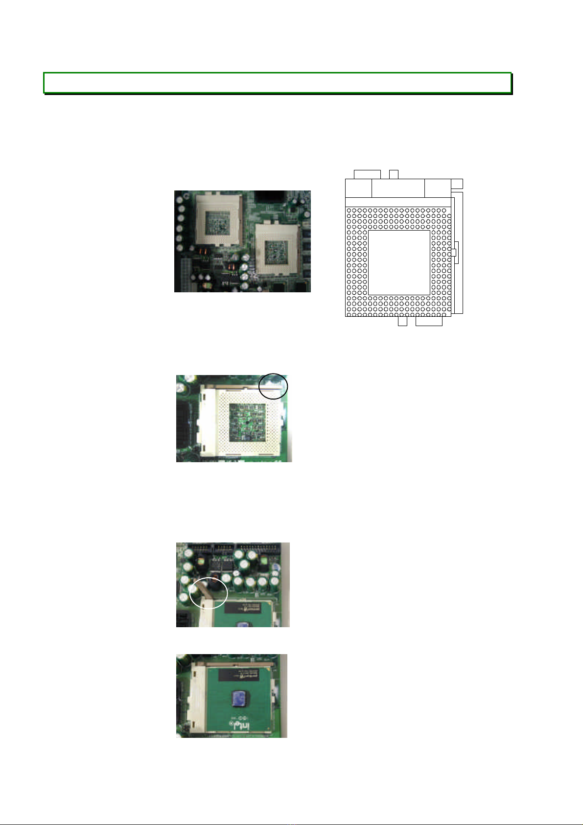
Processor Dual IntelÒ
Pentium III Processor in Socket 370, support FSB
66/100/133 MHz CPU up to 133 MHz x 8 = 1 GHz
Chipset VIA 694X/686B chipset
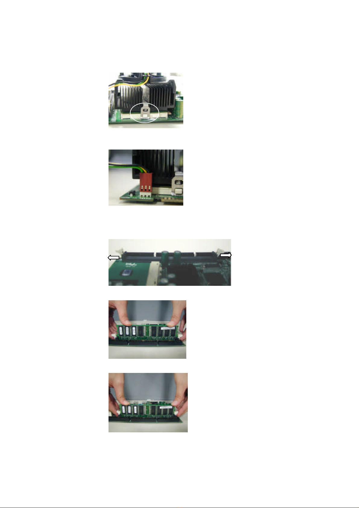
System Memory/RAM Four 168-
pin DIMM sockets, support up to 2 GB SDRAM (Note:
PC100 me
mory support up to 4 DIMMs, PC133 memory support
up to 3 DIMMs)
BIOS AwardÒlicensed BIOS ( 2M bit Flash ROM )
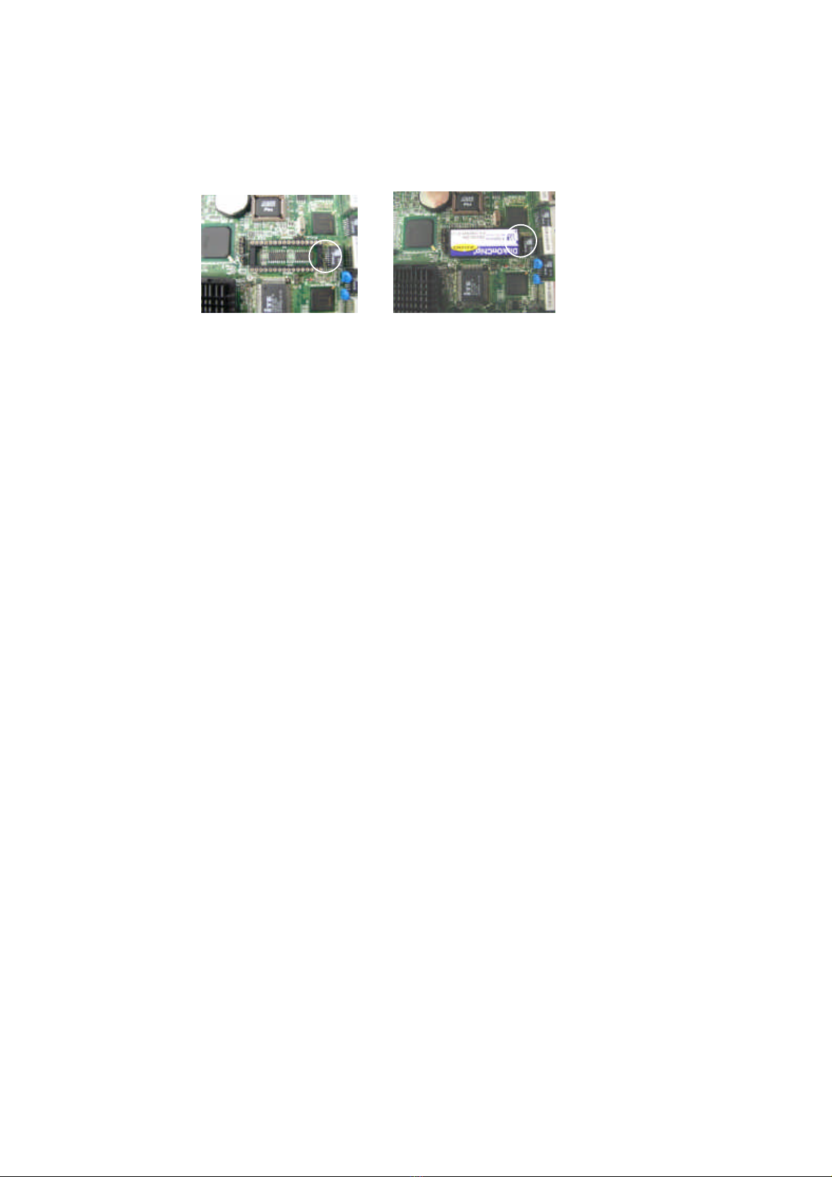
Flash Memory Disk Reserved socket for DiskOnChip from M-
System, support up to
144 MB flash memory disk
AGP VGA Controller ATI Rage XL, with 8MB video memory and DB-15 connector
Sound AC97 codec with 4 phone jacks on rear I/O area
Ethernet Controller Two Intel 82559 chip, support two 10/100M Base-T, on-
board
RJ-45 connector (double stack), support wake on LAN function
IDE Drive Interface Two
PCI IDE port that support up to four IDE devices and Ultra
DMA-33/66/100
Floppy Drive Interface One FDD port, support up to two floppy devices
Serial Port Two COM ports, one RS-232 (DB-9) and one RS-
232/422/485 (pin
header with housing)
Parallel Port One multi-mode parallel port (SPP/EPP/ECP) (DB-25)
Bus Interface Six PCI bus slots
RTC Battery Internal RTC with Li battery
Keyboard/Mouse
Connector: 6-pin mini-Din PS/2 keyboard/mouse connector and 5-
pin
keyboard header
Watchdog Timer 16-level time-out intervals software watchdog timer
Digital I/O 4-bit digital I/O header (10-pin 2.54 mm)
Universal Serial Bus Support two USB connectors
IR Interface Support IrDA header version 1.0
Health Monitoring On-board hardware monitor function
Power Connector ATX power connector (20-
pin) and auxiliary ATX power connector
(6-pin)
Operating Temperature 0 °C~60 °C
Storage Temperature -20 °C~70 °C
Humidity 5 %~95%RH, non-condensing
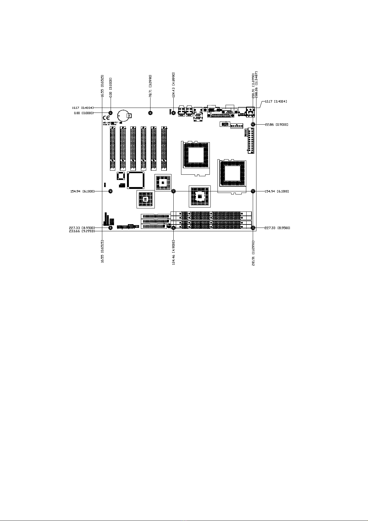
Dimensions 305 x 244 mm ±0.5 mm (12.0” x 9.6”)
Net Weight 500g (1.10 pounds)
1.4 Unpack your MB-X63
Before you begin to install your card, please make sure that you received the following materials
as listed below:
nMB-X63 x1 pc MB-X63 Dual Pentium III Mainboard
nFDD cable x1 set 34-pin to 34-pin standard header flat ribbon cable
nCOM2cable x1 set 10-pin female flat connector header to 9-pin male
D-Sub connector with bracket
nIDE Cable x1 pc DMA-66 IDE cable
nDrivers Utility x1 pc Drivers & Utilities
nUser‘s manual x1 pc This user’s manual

3
1.5 Board Layout

4
CHAPTER 2. Installation
2.1 Hardware Setup and Installation
2.1.1 CPU Installation and Upgrading
Step 1: Locate the ZIF socket and open it by first pulling the lever of socket
upward.
Step 2: Insert the CPU into the socket. Please keep the lever right angle when
inserting CPU.
Step 3: When inserting the CPU please note the correct orientation as shown. The
notched corner should point toward the end of the lever.
Step 4: Push the lever down to close the socket.
PGA370

5
Step5: Attach the heatsink onto the CPU.
Step 6: Push the clip of heatsink downward to hock the ear of socket firmly.
Step 7: Finally, attach the fan cable to the CPU fan header.
2.1.2 System Memory Installation
Step 1: Open latches of DIMM socket.
Step 2: Insert the RAM module into the DIMM socket.
Step 3: Press the latches into the notches of the RAM module.

6
2.1.3 DiskOnChip Installation
Please make sure the central polarization key on the socket, and place the
DiskOnChip as the same direction.

7
2.2 JUMPER SETTINGS AND CONNECTORS
2.2.1 Board Outline
Board Side View
.LAN1VGA1
COM1
USBC1
KM1
CN2
CN1
LPT1
JP4
IRDA1
KCN1
VGA1
COM1
LPT1
USB1
KM1
DIO1
JP1
DIMM 4/3/2/1
PS2
PCI1
PCI2
COM2
FDC1 SC2T2
ISP1
FAN2
SDOC1
SC2T1
PLRS1
JP5
PCI3
PCI4
PCI5
PCI6
FAN1
IDE1/2
CMOS1
SWD1
TWD1
JP2
JP3
LAN1
CN2
CN1
PS1

8
2.2.2 JUMPER SETTINGS SUMMARY
JUMPER FUNCTION
JP2/JP3Default Setup
JP4 ATX POWER ON/OFF Switch
CMOS1 Clear CMOS Data
SWD1 Select Software /Hardware Watch-Dog
TWD1 Select Watch-Dog Time Out Period
JP5 Power LED Connector
SDOC1 Select DiskOnChip ( Flash Disk ) Address
SC2T1, SC2T2 Select COM2 Type
lJP2/JP3: Default Setup
JP2: (1-2)
JP3: (1-2)
lJP4: ATX POWER ON/OFF Switch
lCMOS1 : Clear CMOS Data
CMOS1Description
1-2Normal (Default)
2-3Clear CMOS
1
2
JP4
JP4
Default
1
3
CMOS1
CMOS1
Default
JP2
JP3
Default
1
3
JP2/JP3

9
lSWD1: Select Software /Hardware Watch-Dog
SWD1 Description
ON Hardware (Default)
OFF Software
lTWD1: Select Watch-Dog Time Out Period
TWD1 Time Out Period
1-216 sec
2-364 sec
lJP5: Power LED Connector
Pin Description
1VCC
2NC
3Gnd
1
3
TWD1
TWD1
Default
1
3
JP5
JP5
Default
1
2
SWD1
SWD1
Default

10
lSDOC1: Select DiskOnChip ( Flash Disk ) Address
SDOC1 Flash Disk Address
1-2,9-10 CC00H~CDFFH
3-4,7-8D000H~D1FFH
3-4,9-10 D400h~D5FFH
5-6,7-8D800H~D9FFH
5-6,9-10 DC00H~DDFFH
Default(2-4,8-10)
CC00H~CDFFH
D000H~D1FFH
SDOC1
D400H~D5FFH
D800H~D9FFH
DC00H~DDFFH
2
4
6
8
10
1
3
5
7
9
Default
SDOC1

11
lSC2T1/SC2T2 : Select COM2 Type
COM2 Type SC2T1 SC2T2
RS-232 (Default) 1-21-5,2-6,3-7,4-8
RS-422 3-45-9,6-10,7-11,8-12
RS-485 5-65-9,6-10,7-11,8-12
2.2.3 I/O CONNECTOR SUMMARY
CONNECTOR FUNCTION
ISP1 ISP GAL Connector (Factory only)
KM1 Keyboard/Mouse Connector (Dual Mini-DIN)
IrDA1 Alternate IrDA
VGA1 VGA Connector (D-Sub Connector)
DIO1 Digital Input / Output Ports
JP1 CD_IN
CN1 Lin_in,Mic _in
CN2 Lin_out,Speak _out
PS16 Pin Power Connector
FAN1 Fan Connector
FAN2 Fan Connector
KCN1 KB Connector ( 5-Pin Wafer)
PLRS1 Power LED, Reset, Speaker Connector
COM1 RS232 Serial Port #1 Connector (D-Sub)
COM2 Serial Port #2 Connector (Header)
LPT1 Parallel Port Connector (D-Sub)
PS2ATX Power Connector
FDC1 Floppy Interface Connector (Header)
IDE1 / IDE2 IDE Connector (Header)
RS-422
RS-485
RS-232
1
4
9
10
SC2T2
1
5
2
6
SC2T1
SC2T1
SC2T2
Default

12
lISP1: ISP GAL Connector (Factory only)
Pin No. Description
1VCC
2SDO
3SDI
4ISP
5NC
6MODE
7Ground
8SCLK
lKM1: Keyboard/Mouse Connector (Dual Mini-Din)
Pin No. Description
1KB Data
2NC
3GND
4VCC
5KB CLK
6NC
7MS Data
8NC
9GND
10 VCC
11 MS CLK
12 NC
Mouse
Keyboard
KM1
1
8
ISP1
ISP1

13
lIrDA1: Alternate IrDA
Pin No. Description
1VCC
2NC
3IRRX
4GND
5IRTX
lVGA1: VGA Connector
Pin No. Description
1Red Color Signal
2Green Color Signal
3Blue Color Signal
4NC
5Ground
6Ground
7Ground
8Ground
9NC
10 Ground
11 NC
12 DDC-DATA
13 H-Sync.
14 V-Sync.
15 DDC-CLK
VGA1
5
1
6
10
11
15
IrDA1
1
5
IRDA1
VGA1

14
lDIO1: Digital Input/Output Ports
Pin No. Description
1IN0
2OUT0
3IN1
4OUT1
5IN2
6OUT2
7IN3
8OUT3
9Ground
10 Ground
lJP1: CD_IN
Pin No. Description
1L
2Ground
3Ground
4R
lCN1: Lin_in,Mic _in
CN1 Description
TOP Lin_in
BOTTOM Mic_in
DIO1
DIO1
1
2
9
10
1
4
JP1
CN1
CN1
JP1

15
lCN2: Lin_out,Speak _out
CN2 Description
TOP Lin_out
BOTTOM Speak _out
lPS1: 6 Pin Power Connector
Pin No. Description
1GND
2GND
3GND
43.3V
53.3V
6VCC
lFAN1: FAN Connector
Pin No. Description
1FAN Status
2+12V
3Gnd
FAN1
1
6
PS1
FAN1
1
3
PS1
CN2
CN2

16
lFAN2: FAN Connector
Pin No. Description
1FAN Status
2+12V
3Gnd
lKCN1: KBConnector ( 5-Pin Wafer)
Pin No. Description
1Keyboard Clock
2Keyboard Data
3NC
4GND
5VCC
lPLRS1: Power LED, HDD LED, Reset, Speaker Connector
Pin No. Description
1Power LED +
2GND
3HDD LED +
4HDD LED -
5RESET SW +
6RESET SW –(GND)
7External Speaker -
8Internal Buzzer -
9NC
10 External Speaker +
Default : 7-8(ON) Internal Buzzer
FAN2
1
3
5
1
KCN1
FAN2
KCN1
1
10
PLRS1
PLRS1
Table of contents
Other Lanner electronics Motherboard manuals
Popular Motherboard manuals by other brands

NXP Semiconductors
NXP Semiconductors QorIQ FRDM-LS1012A Reference manual

Asus
Asus F1A55-M LX PLUS R2.0 quick start guide

MSI
MSI X299 TOMAHAWK ARCTIC quick start

National Semiconductor
National Semiconductor ADC14DC105 user guide

Cypress Semiconductor
Cypress Semiconductor CapSense CY8CKIT-024 Guide

Team Orion
Team Orion Vortex DSB-R+ instruction manual

Silicon Laboratories
Silicon Laboratories Si80xx-EVB user guide

Nvidia
Nvidia nForce 680I LT SLI user manual

Gigabyte
Gigabyte GA-H81M-S2VP user manual

Congatec
Congatec COM Express conga-TR3 user guide

Texas Instruments
Texas Instruments J721E user guide

EPH Controls
EPH Controls R27-RF operating instructions