L1512S Service Manual
-6- 10/24/2002
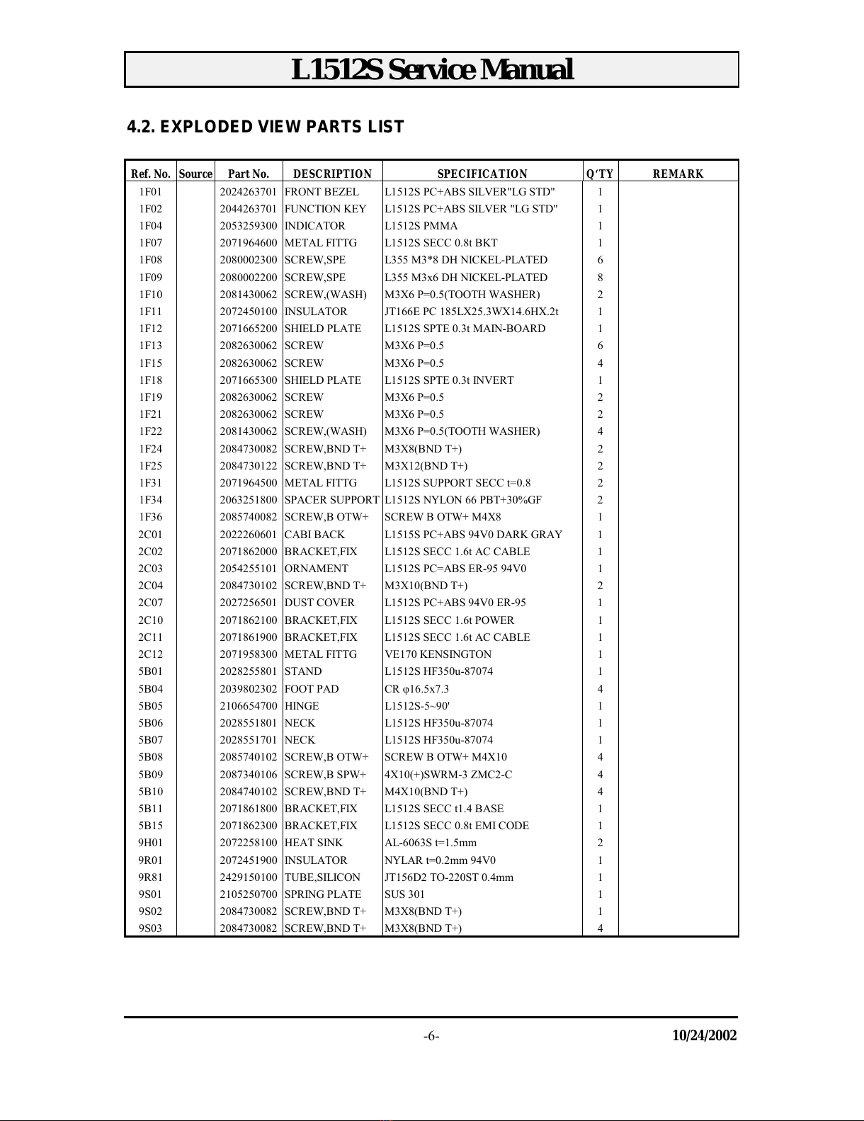
4.2. EXPLODED VIEW PARTS LIST
Ref. No. Source Part No. DESCRIPTION SPECIFICATION Q‘TY REMARK
1F01 2024263701 FRONT BEZEL L1512S PC+ABS SILVER"LG STD" 1
1F02 2044263701 FUNCTION KEY L1512S PC+ABS SILVER "LG STD" 1
1F04 2053259300 INDICATOR L1512S PMMA 1
1F07 2071964600 METAL FITTG L1512S SECC 0.8t BKT 1
1F08 2080002300 SCREW,SPE L355 M3*8 DH NICKEL-PLATED 6
1F09 2080002200 SCREW,SPE L355 M3x6 DH NICKEL-PLATED 8
1F10 2081430062 SCREW,(WASH) M3X6 P=0.5(TOOTH WASHER) 2
1F11 2072450100 INSULATOR JT166E PC 185LX25.3WX14.6HX.2t 1
1F12 2071665200 SHIELD PLATE L1512S SPTE 0.3t MAIN-BOARD 1
1F13 2082630062 SCREW M3X6 P=0.5 6
1F15 2082630062 SCREW M3X6 P=0.5 4
1F18 2071665300 SHIELD PLATE L1512S SPTE 0.3t INVERT 1
1F19 2082630062 SCREW M3X6 P=0.5 2
1F21 2082630062 SCREW M3X6 P=0.5 2
1F22 2081430062 SCREW,(WASH) M3X6 P=0.5(TOOTH WASHER) 4
1F24 2084730082 SCREW,BND T+ M3X8(BND T+) 2
1F25 2084730122 SCREW,BND T+ M3X12(BND T+) 2
1F31 2071964500 METAL FITTG L1512S SUPPORT SECC t=0.8 2
1F34 2063251800 SPACER SUPPORT L1512S NYLON 66 PBT+30%GF 2
1F36 2085740082 SCREW,B OTW+ SCREW B OTW+ M4X8 1
2C01 2022260601 CABI BACK L1515S PC+ABS 94V0 DARK GRAY 1
2C02 2071862000 BRACKET,FIX L1512S SECC 1.6t AC CABLE 1
2C03 2054255101 ORNAMENT L1512S PC=ABS ER-95 94V0 1
2C04 2084730102 SCREW,BND T+ M3X10(BND T+) 2
2C07 2027256501 DUST COVER L1512S PC+ABS 94V0 ER-95 1
2C10 2071862100 BRACKET,FIX L1512S SECC 1.6t POWER 1
2C11 2071861900 BRACKET,FIX L1512S SECC 1.6t AC CABLE 1
2C12 2071958300 METAL FITTG VE170 KENSINGTON 1
5B01 2028255801 STAND L1512S HF350u-87074 1
5B04 2039802302 FOOT PAD CR φ16.5x7.3 4
5B05 2106654700 HINGE L1512S-5~90' 1
5B06 2028551801 NECK L1512S HF350u-87074 1
5B07 2028551701 NECK L1512S HF350u-87074 1
5B08 2085740102 SCREW,B OTW+ SCREW B OTW+ M4X10 4
5B09 2087340106 SCREW,B SPW+ 4X10(+)SWRM-3 ZMC2-C 4
5B10 2084740102 SCREW,BND T+ M4X10(BND T+) 4
5B11 2071861800 BRACKET,FIX L1512S SECC t1.4 BASE 1
5B15 2071862300 BRACKET,FIX L1512S SECC 0.8t EMI CODE 1
9H01 2072258100 HEAT SINK AL-6063S t=1.5mm 2
9R01 2072451900 INSULATOR NYLAR t=0.2mm 94V0 1
9R81 2429150100 TUBE,SILICON JT156D2 TO-220ST 0.4mm 1
9S01 2105250700 SPRING PLATE SUS 301 1
9S02 2084730082 SCREW,BND T+ M3X8(BND T+) 1
9S03 2084730082 SCREW,BND T+ M3X8(BND T+) 4