LG 50PC52 User manual

PLASMA TV
SERVICE MANUAL
CAUTION
BEFORE SERVICING THE CHASSIS,
READ THE SAFETY PRECAUTIONS IN THIS MANUAL.
CHASSIS : PP78A
MODEL : 50PC52 50PC52-ZD
website:htt ://biz.LGservice.com

- 2 -
CONTENTS
CONTENTS .............................................................................................. 2
SAFETY PRECAUTIONS ..........................................................................3
SPECIFICATION ........................................................................................4
ADJUSTMENT INSTRUCTION .................................................................6
TROUBLE SHOOTING ............................................................................15
BLOCK DIAGRAM...................................................................................23
EXPLODED VIE .................................................................................. 24
EXPLODED VIE PARTS LIST ............................................................ 25
REPLACEMENT PARTS LIST ............................................................... 26
SVC. SHEET ...............................................................................................
PRINTED CIRCUIT DIAGRAM ....................................................................

- 3 -
SAFETY PRECAUTIONS
Many electrical and mechanical parts in this chassis have special safety-related characteristics. These parts are identified by in the
Schematic Diagram and Replacement Parts List.
It is essential that these special safety parts sh uld be replaced with the same c mp nents as rec mmended in this manual t prevent
X-RADIATION, Sh ck, Fire, r ther Hazards.
D n t m dify the riginal design with ut permissi n f manufacturer.
General Guidance
An isolation Transformer should always be used during the
servicing f a receiver wh se chassis is n t is lated fr m the AC
p wer line. Use a transf rmer f adequate p wer rating as this
pr tects the technician fr m accidents resulting in pers nal injury
fr m electrical sh cks.
It will als pr tect the receiver and it's c mp nents fr m being
damaged by accidental sh rts f the circuitry that may be
inadvertently intr duced during the service perati n.
If any fuse ( r Fusible Resist r) in this m nit r is bl wn, replace it
with the specified.
When replacing a high wattage resist r (Oxide Metal Film Resist r,
ver 1W), keep the resist r 10mm away fr m PCB.
Keep wires away fr m high v ltage r high temperature parts.
Due t high vacuum and large surface area f picture tube,
extreme care sh uld be used in handling the Picture Tube.
D n t lift the Picture tube by it's Neck.
Leakage Current Cold Check(Antenna Cold Check)
With the instrument AC plug rem ved fr m AC s urce, c nnect an
electrical jumper acr ss the tw AC plug pr ngs. Place the AC
switch in the n p siti n, c nnect ne lead f hm-meter t the AC
plug pr ngs tied t gether and t uch ther hm-meter lead in turn t
each exp sed metallic parts such as antenna terminals, ph ne
jacks, etc.
If the exp sed metallic part has a return path t the chassis, the
measured resistance sh uld be between 1MΩ and 5.2MΩ.
When the exp sed metal has n return path t the chassis the
reading must be infinite.
An ther abn rmality exists that must be c rrected bef re the
receiver is returned t the cust mer.
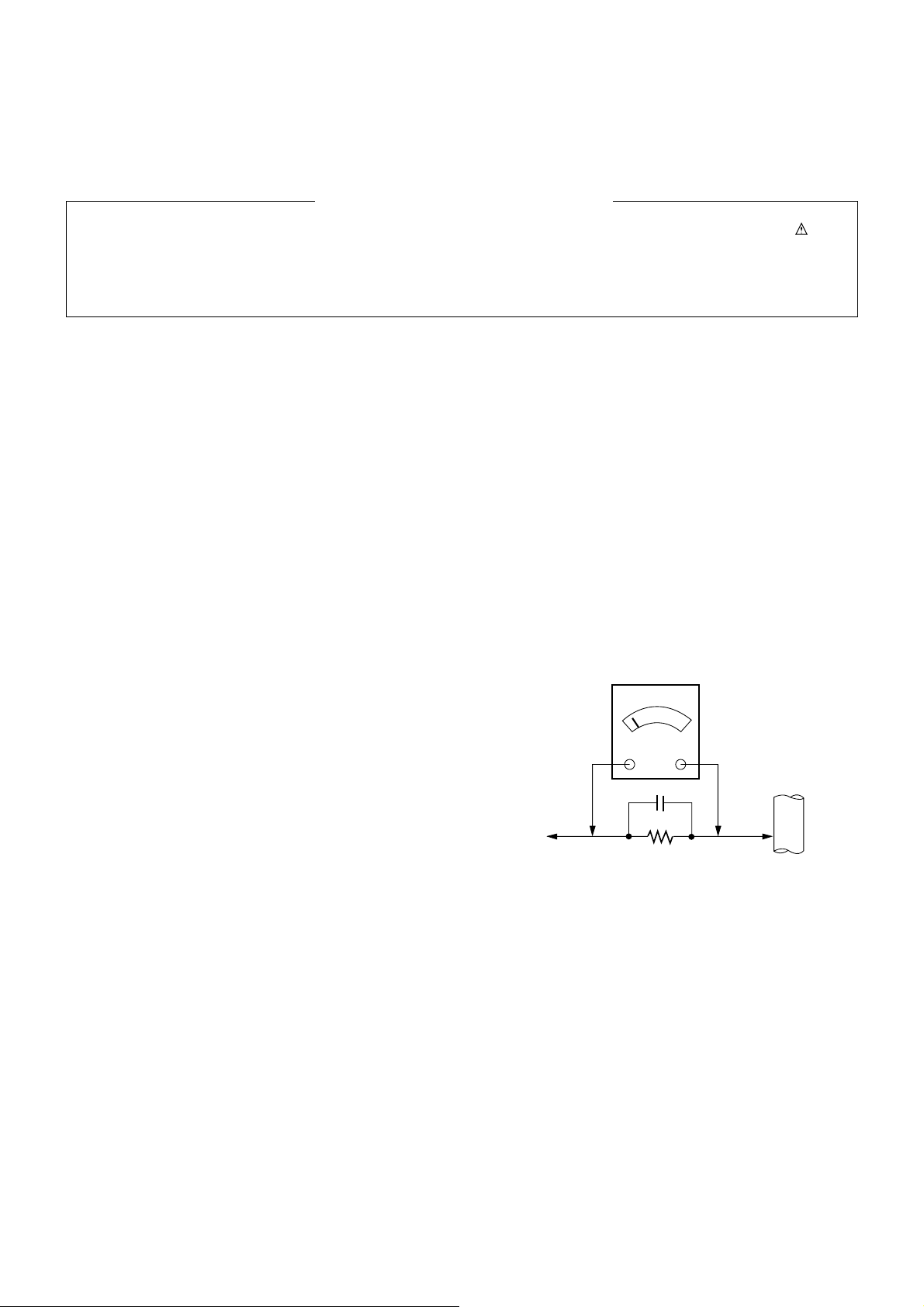
Leakage Current Hot Check (See below Figure)
Plug the AC c rd directly int the AC utlet.
Do not use a line Isolation Transformer during this check.
C nnect 1.5K/10watt resist r in parallel with a 0.15uF capacit r
between a kn wn g d earth gr und (Water Pipe, C nduit, etc.)
and the exp sed metallic parts.
Measure the AC v ltage acr ss the resist r using AC v ltmeter
with 1000 hms/v lt r m re sensitivity.
Reverse plug the AC c rd int the AC utlet and repeat AC v ltage
measurements f r each exp sed metallic part. Any v ltage
measured must n t exceed 0.75 v lt RMS which is c rresp nds t
0.5mA.
In case any measurement is ut f the limits specified, there is
p ssibility f sh ck hazard and the set must be checked and
repaired bef re it is returned t the cust mer.
Leakage Current Hot Check circuit
1.5 K hm/10W
T Instrument's
exp sed
METALLIC PARTS
G d Earth Gr und
such as WATER PIPE,
CONDUIT etc.
AC V lt-meter
IMPORTANT SAFETY NOTICE
0.15uF

- 4 -
SPECIFICATIONS
NOTE : Specificati ns and thers are subject t change with ut n tice f r impr vement
.
VApplication Range
This spec is applied t the 50” PLASMA TV used PP78A Chassis.
V Specification
Each part is tested as bel w with ut special app intment.
1) Temperature : 25±5°C (77±9°F), CST : 40±5
2) Relative Humidity: 65±10%
3) P wer V ltage: Standard Input v ltage (100-240V~, 50/60Hz)
* Standard V ltage f each pr duct is marked by m dels.
4) Specificati n and perf rmance f each parts are f ll wed each drawing and specificati n by part number in acc rdance with SBOM.
5) The receiver must be perated f r ab ut 20 minutes pri r t the adjustment.
VTest Method
1) Perf rmance : LGE TV test meth d f ll wed.
2) Demanded ther specificati n
Safety : CE, IEC specificati n
EMC : CE, IEC
VGeneral Specification ( 50”XGA )
Chassis
PP78A 50PC52-ZD EU LG
M del Name Market Brand Remark
50PC52-ZD Safety : IEC/EN60065, EMI : EN55013, EMS : EN55020EU
M del ApplianceMarket
TEST
Remark
Display Screen Device
Aspect Rati
PDP M dule
Operating Envir nment
St rage Envir nment
Input V ltage
1
2
3
4
5
6
N Item Specificati n Remark
50” Wide C l r Display M dule
16:9
PDP50X4,
RGB Cl sed Type
1)Temp. : 0~40deg
2)Humidity : 0~85%
3)Temp. : -20~60deg
4)Humidity : 0~85%
100-240V~, 50/60Hz
Plasma Display Panel
Clear Filter
LGE SPEC.
Maker : Sanken

- 5 -
VModule Specification2
Market
Br adcasting system
Available Channel
Receiving system
SCART Jack(2EA)
Vide Input (1EA)
S-Vide Input (1EA)
C mp nent Input (1EA)
RGB Input(1EA)
HDMI Input(1EA)
Audi Input (5EA)
Audi variable ut(1EA)
1
2
3
4
5
6
7
8
9
10
11
12
N Item Specificati n Remark
EU
PAL-BG/I/DK, NTSC, SECAM
BAND PAL
VHF/UHF C1~C69
CATV S1~S47
Upper Heter dyne
PAL, SECAM, NTSC
PAL, SECAM, NTSC
PAL, SECAM, NTSC
Y/Cb/Cr, Y/Pb/Pr
RGB-PC
HDMI-DTV
PC Audi , C mp nent(1EA),
AV (2EA), SIDE AV(1EA)
FULL SCART, HALF SCART
SIDE AV
SIDE S-VIDEO
L/R Input
VModule Specification (PDP50X4)
Display area
Outline dimensi n
Number f Pixels
Cell pitch
C l r arrangement
Weight(net)
Temperature
Operating Envir nment Humidity
Pressure
Temperature
St rage Envir nment Humidity
Pressure
Image stick Start time
minimizati n L w Brightness Arrival Time
m de
1106.5 (H) * 662.1(V)±0.5
1190 (W) x 700 (H) x 52 (D)±1
1366 (H) x 768(V)
270um (H) x 810um (V)
RGB cl sed type
13.8 14.3 14.8
0 ~ 40
20 ~ 80
800 ~ 1100
-20 ~ 60
10 ~ 90
700 ~ 1100
4.5 5 5.5
14 16 16
1
2
3
4
5
6
7
8
9
N Item Remark
1Pixel=3RGB Cells
1Pixel=3RGB Cells
Altitude : 0 t 2000M
Altitude : 0 t 3000M
mm
mm
um
Kg
deg
%
hPa
deg
%
hPa
min
min
Min Typ Max Unit

- 6 -
ADJUSTMENT INSTRUCTION
1. Application Object
These instructi ns are applied t all f the 50” PLASMA TV,
PP78A Chassis.
2. Note
(1) Because this is n t a h t chassis, it is n t necessary t use
an is lati n transf rmer. H wever, the use f is lati n
transf rmer will help pr tect test instrument.
(2) Adjustment must be d ne in the c rrect rder.
(3) The adjustment must be perf rmed in the circumstance f
25±5°C f temperature and 65±10% f relative humidity if
there is n specific designati n.
(4) The input v ltage f the receiver must keep 100-220V~,
50/60Hz.
(5) Bef re adjustment, execute Heat Run f r 30 minutes.
3. Adjustment items
3.1. PCB assembly adjustment items
(1) D wnl ad the VCTP main s ftware (IC500,VCT_Pr )
(2) Channel mem ry (IC501,EEPROM)
(3) C l r carrier Adjustment
3.2. SET assembly adjustment items
(1) DDC Data input.
(2) Adjustment f White Balance.
(3) Fact ring Opti n Data input.
4. PCB assembly adjustment method
(Using VCTP Download program)
4-1. Download program installation
(1) Extract a Zip file.
(2) Visual I2C & LPT Driver Installati n.
LPT P rt Driver (LptDrv) Setups : Pr gram Files > Micr nas >
Visual I2C > P rt_Driver
*Use f r Wind ws 95/98 : Setup_LptDrv_v0104_9x.exe
*Use f r Wind ws 2000/XP : Setup_LptDrv_v0202_XP_2000.exe
*
Use f r Wind ws NT : Setup_LptDrv_v0104_NT.exe
(3) Verificati n.(Start > Pr grams > Micr nas > Visual I2C r
LptDrv)
(4) LPT delay setting.(File > Preference > LPT preferences)
(5) Exchange the “b tl ader.bat” file.
Click the red area
D uble click the Red
Install the LPT Driver
Install the Visual I2C
*LPT SETTING
- Delay => 1
- Time ut => 500 ms

- 7 -
=> Select the "B tl ader.bat" file.
(install > VCTP_d wnl ad > B tl ader)
=> Push "OK".
=>
Finish the pr gram, after saving the file "d wnl ad_cs.vi2c".
(if y u click , the massage appears aut matically)
5. S/ program download
5-1. Profile
: This is f r d wnl ading the s/w t the flash mem ry f the
vctp(IC500)
5-2. Required Test Equipment
(1) PC.
(2) Visual IIC pr gram.
(3) D wnl ad jig.
5-3. Connection structure
6. Download method
6-1. Download method 1 (PCB Ass’y)
(1) C nnect the d wnl ad jig t D-sub jack.
(2) Execute ‘D wnl ad.vi2c’ pr gram in PC, then a main
wind w will be pened.
(3)
D uble click the blue b x and c nfirm "B tl ader Versi n" as 42.
(4) Click the "Erase Flash" butt n.
(5) D uble click the d wnl ad file l w, then "edit" wind w will
be pened.
(6) Click the ch ice butt n in the “edit wind w”, then “file
ch ice wind w” will be pened.
(7) Ch se the Hex file in f lder and execute d wnl ading
with click " pen" butt n.
x
Y u must verify the w rds f “0xfffff” in the black b x f figure.
(In case f H3 Service it is 0x7ffff : If y u make H4 service after
the H3 service, there c uld be s me pr blem)

- 8 -
(8) Click OK butt n at the "edit wind w".
(9) Under D wnl ading pr cess.
(10) If d wnl ad is failed, f r example "N ackn wledge fr m
slave". Execute d wnl ad again fr m(1).
6-2.Download method 2 (AV Plate Ass’y)
(1) Push S/W ‘ON" (c nnect SCL t GND using switch at Jig )
and c nnect the d wnl ad jig t D-sub jack.
(2) Supply the p wer (Stand-by 5V) and wait f r 3 sec nds.
(3)
Push the S/W ff.(Disc nnect SCL t GND using switch at jig).
(4) Execute ‘D wnl ad.vi2c’ pr gram in PC, then a main
wid w will be pened.
(5)
D uble click the blue b x and c nfirm "B tl ader Versi n" as 42
.
(6) Click the "Erase Flash" butt n.
(7) D uble click the d wnl ad file l w then, "edit" wind w will
be pened.
(8) Chick the ch ice butt n I n the "edit wind w", then "file
ch ice wind w’ will be pened.
(9) Click the “l ad > flash” butt n.
(10) Ch se the Hex file in f lder and execute d wnl ading
with click " pen butt n".
Push S/W
Push S/W
A
Y u must verify the w rds f “0xfffff” in the black b x(A) f figure.
(In case f H3 Service it is 0x7ffff : If y u make H4 service after
the H3 service, there c uld be s me pr blem)

- 9 -
(11) Click OK butt n at the "edit wind w".
(12) Under D wnl ading pr gress.
(13) If d wnl ad is failed, f r example "N ackn wledge fr m
slave", execute d wnl ad again fr m (1).
6-3.Download method 3 (SET)
(1) Push the “Tilt” butt n in an Adjust Rem c n Then the
PLASMA TV will change a “slave m de”.
(2) C nnect Zig t TV using a D-sub cable.
(3) Execute ‘D wnl ad_CS.vi2c’ pr gram in PC, then a main
wid w will be pened.
(4) Click "GO" butt n.
If y u d n’t push the “g ”, the Hex file w uld n t be
d wnl aded alth ugh the d wnl ad pr ceeds n rmally at
first glance.
(5) D uble click the blue b x and c nfirm "B tl ader
Versi n" as 42.
(6) Click the "Erase Flash" butt n.
(7) D uble click the d wnl ad file l w then, "edit" wind w will
be pened.
(8) Chick the ch ice butt n I n the "edit wind w", then "file
ch ice wind w’ will be pened.
(9) Click the “l ad > flash” butt n.
A
Y u must verify the w rds f “0xfffff” in the black b x(A) f figure.
(In case f H3 Service it is 0x7ffff : If y u make H4 service after
the H3 service, there c uld be s me pr blem)

- 10 -
(10) Ch se the Hex file in f lder and execute d wnl ading
with click " pen butt n".
(11) Click OK butt n at the "edit wind w".
(12) Under D wnl ading pr gress.
(13) If d wnl ad is failed, f r example "N ackn wledge fr m
slave", execute d wnl ad again fr m (1).
7. Channel memory download
7-1. Profile
: This is f r d wnl ading the s/w t the flash mem ry f the
vctp(IC500)
7-2. Required Test Equipment
(1) PC.
(2) Visual IIC pr gram.
(3) D wnl ad jig.
7-3. Connection structure
(1) C nnect the d wnl ad jig t D-sub jack.
(2) Execute ‘Channel.vi2c’ pr gram in PC, then a main
wind w will be pened.
7-4. Connection condition
(1) IC name and circuit number : VCTP and IC500.
(2) Use v ltage : 3.3V.
(3) SCL : 15pin.
(4) SDA : 12pin.
(5) Tact time : ab ut 3sec nds.
7-5. Download method
(1) C nnect the d wnl ad jig t D-sub jack.
(2) ‘Execute ‘Channel vi2c’ pr gram in PC, then a main
wind w will be pened.
(3) Push the butt n change and select the Channel mem ry
data.
(4) Check the c mmunicati n is OK r n t.
=> Push the Read area (Ackn. Check) and check Cyan area
is OK message.
(5) Push the Update NVM fr m File

- 11 -
8. Tool Option Area Option Change
8-1. Profile
:
Must be changed the pti n value because being different with
s me setting value depend n m dule, inch and market.
8-2. Required Test Equipment
1) Adjustment rem c n.
8-3. Adjustment method
Bef re PCB check, have t change the T l pti n and Area pti n.
Opti n values are bel w.
(If n changed the pti n, the input menu can differ the m del spec.)
The input meth ds are same as ther chassises.(Use adj Key
n the Adjust Rem c n)
* After d ne all adjustments, Press ADJ butt n and c mpare
T l pti n and Area pti n value with its BOM, if it is
c rrectly same then unplug the AC cable.
If it is n t same, then c rrect it same with BOM and unplug AC cable.
F r c rrect it t the m del’s m dule fr m fact ry JIG m del.
9. Color carrier Adjustment
(Inspection process)
9-1. Profile
: T have the margin ab ut the deviati n f c l r carrier t
satisfy the spec.
9-2. Required Test Equipment
1) Adjustment rem c n.
2) Pal RF signal.
9-3. Connection
: TV set sh uld c nnected with the pal RF signal(EU 5CH).
9-4. Adjustment method
(1) tuning the RF signal
ZA/ZB, TA/TB : PAL Philips Pattern (with C l r Bar)
(2) push the “adj” key in the adjustment rem c n.
10. PO ER PCB Assy Voltage
Adjustments (Va, Vs V ltage adjustments)
10-1. Profile
: T supply the Va, Vs v ltage that the m dule want.
10-2. Required Test Equipment
(1) Stick f r adjustment.
(2) DMM.
10-3. Connection structure
10-4. Connection Diagram for Measuring
: refer t (Fig. 1)
10-5. Adjustment Method
(1) Va Adjustment
1) After receiving 100% Full White Pattern, HEAT RUN.
2) C nnect + terminal f D. M..M. t Va pin f P812, c nnect
-terminal t GND pin f P812.
3)
After turning VR901,v ltage f D.M.M adjustment as
same as Va v ltage which n label f panel right/t p.
(deviati n;
±
0.5V)
(2) Vs Adjustment
1) C nnect + terminal f D. M..M. t Vs pin f P812, c nnect
-terminal t GND pin f P812.
2)
After turning VR951, v ltage f D.M.M adjustment as
same as Vs v ltage which n label f panel right/t p.
(deviati n ; ±0.5V)
Each PCB assembly must be checked by check JIG set.
(Because p wer PCB Assembly damages t PDP M dule,
especially be careful)
50
PC5R
PC6R
PC7R
PB3R
TOOL OPTION ZA/ZB TA/TB
2260
2516
2772
3028
4308
4564
4820
5076
(Fig. 1) C nnecti n Diagram f p wer adjustment f r measuring.

11. EDID(The Extended Display Identification Data )
/DDC(Display Data Channel) download
11-1. Profile
: T be p ssible f r plug and play.
11-2. Required Test Equipment
(1) Adjusting PC with S/W f r writing EDID Data.
(S/W : EDID TESTER Ver.2.5)
(2) A Jig f r EDID D wnl ad.
(3) Cable : Serial(9Pin r USB) t D-sub 15Pin cable, D-sub
15Pin cable, DVI t HDMI cable.
11-3. Connection structure
* Cauti n
- Never c nnect HDMI & D-SUB Cable at the same time.
- Use the pr per cables bel w f r EDID Writing.
11-4. Preparation for Adjustment
(1) As ab ve (Fig. 2), C nnect the Set, EDID D wnl ad Jig,
PC & Cable.
(2) Turn n the PC & EDID D wnl ad Jig. And Execute the
S/W : EDID TESTER Ver 2.5.
(3) Set up S/W pti n.
Repeat Number : 5
Device Address : A0
PageByte : 8
(4) P wer n the Set.
11-5. Sequence of Adjustment
(1) DDC data f Anal g-RGB
1) Init the data.
2) L ad the EDID data.(Open File).
[ Anal g
-
RGB
: PP78A_RGB.ANA ]
[ Digital-HDMI1 :
PP78A_HDMI1.DVI ]
[ Digital-HDMI2 :
PP78A_HDMI2.DVI ]
3) Set the S/W as bel w.
(4) Push the “Write Data & Verify”butt n. And c nfirm “Yes”.
(5) If the writing is finished, y u will see the “OK” message.
- 12 -
F r RGB EDID F r HDMI EDID
(Fig. 2) C nnecti n Diagram f DDC d wnl ad
Open FileOpen File

- 13 -
11-6. EDID Data
(1) XGA
<Anal g (RGB) >
< Digital1 (HDMI/DVI1) >
< Digital2 (HDMI/DVI2) >
=> Detail EDID Opti ns are bel w(1,2,3,4,5)
1. Pr duct ID
2. Serial N : C ntr lled n pr ducti n line
3. M nth, Year : C ntr lled n pr ducti n line
ex) M nthly: '03' => '03'
Year: '2005' => '0F'
4. M del Name : m del name -> LG TV
- LG TV
5. Checksum (7EH) -> Changeable by t tal EDID data.
12. Adjustment of hite Balance
12-1. Purpose and Principle for adjustment
of the color temperature
(1) Purp se : Adjust the c l r temperature t reduce the
deviati n f the m dule c l r temperature.
(2) Principle : T adjust the white balance with ut the
saturati n, Fix the ne f R/G/B gain t 80 and decrease
the thers.
12-2.Adjustment mode
: Tw m des f C l and Warm.(Medium data is
aut matically calibrated by the c l data)
12-3. Required Equipment
(1) Rem te c ntr l f r adjustment.
(2) C l r Analyzer.(CA-110 r same pr duct) - CH : 10
(3) Aut W/B adjustment instrument.( nly f r Aut adjustment)
12-4. Connecting diagram of equipment for
measuring (For Automatic Adjustment)
(1) Enter the DDC adjust m de.
- Enter the white balance adjustment m de at the same
time heat-run m de when pushing the p wer n by p wer
nly key.
- Maintain the white balance adjustment m de with same
c nditi n f Heat-run.
->
Maintain after AC ff/ n in status f Heat-run pattern display.
(2) Release the DDC adjust m de.
- Release the adjust m de after AC ff/ n r std-by ff/ n
in status f finishing the Hear-run m de.
- Release the Adjust m de when receiving the aging ff
c mmand(F3 00 00) fr m adjustment equipment.
- Need t transmit the aging ff c mmand t TV set after
finishing the adjustment.
* Standard c l r c rdinate and temperature when using the
CA-110 r CA210 equipment.
* Synchr nizati n relati n between PSM and CSM.
M del
Name
50PC5R
(50PC51/52)
DEC
50007 (A)
50008 (D)
Pr duct ID
HEX
C357
C358
EDID table
57C3
58C3 C l r C rdinate
xy
0.283±0.002
0.293±0.002
0.329±0.00
2
11,000K
9,300K
6,500K
0.000
0.000
0.003
0.276±0.002
0.285±0.002
0.313±0.00
2
COOL
MEDIUM
WARM
M de Temp uv
CSM Remark
C l
N rmal
Warm
Dynamic
Standard
Mild
PSM
12
3
4
4 5
1 2
3
4
4
5
5
12
3
4
4
5
5

- 14 -
(3) DDC adjustment supp rt c mmand set.
* R/G/B GAIN max value : 80
12-5. Adjustment of hite Balance
(For Manual adjustment)
- Adjustment m de : Tw m des f C l (Dynamic) and
Warm(Mild).
(Medium data is aut matically calibrated by the c l data)
- C l r analyzer(CA110, CA210) sh uld be used in the
calibrated ch by CS-1000.(PDP : CH10)
- Operate the zer -calibrati n f the CA-110 r CA-210, then
stick sens r t the m dule when adjusting.
- F r manual adjustment, it is als p ssible by the f ll wing
sequence.
(1) Select RF n signal by pressing “PO ER ON” key n
rem te c ntr l f r adjustment then perate heat run m re
than 15 minutes.
(If n t executed this step, the c nditi n f r W/B will be differ.)
(2) Changing t the av m de by pushing the input r fr nt av
key.(av m de : av1 r av2 r av3)
(3) Display the internal pattern f the VCT-Pr IC by pushing
the IN-START.
(4) Stick sens r t center f the screen and select each items
(Red/Green/Blue Gain and Offset) using D/E (CH+/-) key
n R/C.
(5) Adjust R Gain / B Gain using F/G(VOL+/-) key n R/C.
(6) Adjust tw m des f C l(Dynamic) and Warm(Mild) as
bel w figure.
(Fix the ne f R/G/B and change the thers)
1. Push the ne time the in-start key : Dynamic(C l)
2. Push the tw m re the in-start key : Mild(Warm)
* Refer t the bel w case t kn w what value is fixed.
* CASE
- First adjust the c rdinate much away fr m the target
value(x, y).
1) x, y > target
(1) Decrease the R, G.
2) x, y < target
(1) First decrease the B gain.
(2) Decrease the ne f the thers.
- In case f decreasing the x, decreasing the R : fix G
- In case f decreasing the y , decreasing the G : fix R
3) x > target , y < target
(1) First decrease B, s make y a little m re than the
target.
(2) Adjust x value by decreasing the R.
4) x < target , y > target
(1) First decrease B, s make x a little m re than the
target.
(2) Adjust x value by decreasing the G.
(7) When adjustment is c mpleted, Exit adjustment m de
using EXIT key n R/C.
13. Input the Shipping Option Data
(1) Push the ADJ key in a Adjust Rem te c ntr l.
(2) Input the Opti n Number that was specified in the BOM,
int the Shipping area.
(3) The w rk is finished, Push AKey.
14. Default Value in Adjustment mode
(Default values maybe modified the module condition)
14-1. hite Balance
15. Internal press test
16. Sound spec.
Adjustment
Aging On/Off
Input select
R GAIN
G GAIN
B GAIN
R GAIN
G GAIN
B GAIN
R GAIN
G GAIN
B GAIN
CMD(HEX)
F3
F4
16
18
1A
16
18
1A
16
18
1A
ADR
00
00
00
01
02
VALUE
FF/00
00 - FE
00 - FE
00 - FE
00 - FE
00 - FE
00 - FE
00 - FE
00 - FE
00 - FE
Detail
OO : OFF
01 : ON
FF : WB Ready
0x10 : TV
0x20 : AV1
0x21 : AV2
0x23 : AV3
0x40 : C mp nent1
0x50 : RGB DTV
0x60 : RGB PC
0x90 : HDMI1 DTV
GAIN adjustment
CSM COOL
GAIN adjustment
CSM NORMAL
GAIN adjustment
CSM WARM
C l r C rdinate
xy
0.283±0.002
0.293±0.002
0.329±0.00
2
11,000K
9,300K
6,500K
0.000
0.000
0.003
0.276±0.002
0.285±0.002
0.313±0.00
2
COOL
MEDIUM
WARM
M de Temp uv
Item
Dielectric V ltage (AC <-> FG)
Dielectric V ltage (With ut FG)
Value
1.5
1.5
3
3
Unit
kV
kV
Remark
At 100mA f r 1sec (Line)
At 100mA f r 1min (OQC)
At 100mA f r 1sec (Line)
At 100mA f r 1min (OQC)
Item Min Typ Max Unit Remark
Audi Practical Max Output, L(M n )/R 9 10 12 W PDP
<Default Value n OSD>

- 15 -
TROUBLESHOOTING
1. No power
(1) Symptom
1) Minute discharge d es n t ccur at m dule.
2) Fr nt LED d es n t activate.
(2) Press check
Plug in the p wer c rd
Start Check
N
Yes
Is the p wer c rd
plugged in?
C nnect the cable.
Plasma(CN1)
N
Yes
Are the line filter and
PSU c nnected?
Replace the fuse.
N
Yes
Is the c rrect fuse f r
the PSU in place?
Plasma(F101)
C nnect the 13-14pin cable.
Next rem ve all cables c nnected t the PSU and
switch the AV v ltage t manual.
If the ST-by 5V d es n t perate, replace the PSU.
N
Yes
Is the PSU and 13-
14pin cable c nnected
t the VSC b ard?

- 16 -
2. Protect mode
(1) Symptom
1) After lighting nce it d es n t discharge minutely fr m the m dule.
2) The relay falls.(there is an audible “Click”.)
3) The c l r f the fr nt LED turns fr m green t red.
(2) Follow check
Is the P wer B ard
n rmal ?
Replace P wer B ard.
Is the utput the n rmal L w/High
v ltage except f r the Stand-by 5V?
Yes
N N
Are all the c nnect rs
n rmal?
Replace the c nnect r.
Replace the fuse.
Replace the Y-B ard.
After checking each c nnect r d es
is perate c rrectly?
Yes
N N
Is the Y-B ard
n rmal?
Is the appr priate
fuse (FS2,FS3) n the
Y-B/D?
Is the utput v ltage
n rmal after rem ving the
P1 c nnect r f the Y-B/D?
Yes
N N
Replace the Z-B ard.
Is the Z-B ard
n rmal?
Is appr priate
fuse (FS1,FS2) n
the Z-B/D?
Is the utput v ltage
n rmal after rem ving the
P1 c nnect r f the Z-B/D?
Yes
N N
Is the X- B ard
n rmal?
Is the
utput v ltage n rmal
after rem ving the P100, 110,
200, 210 c nnect r f
the X-B/D?
After rem ving the P100, 110 and the utput
v ltage is n rmal : Replace the Right X-B/D
After rem ving the P200, 210 and the utput
v ltage is n rmal : Replace the Left X-B/D
N
Yes
Replace the fuse.
Yes
Start Check

- 17 -
3. No Raster
(1) Symptom
1) N OSD r image are displayed n the screen.
2) The fr nt LED remains green.
(2) Follow check
4. In the case an unusual display in RF mode.
Check the PDP M dule
Replace the
P wer b ard.
D es
minute discharge
at M dule?
Is the inverter
/VaVs n?
Is utput the n rmal
L w/High v ltage except
f r the Stand-by 5V?
Yes
N N
Is there a fault with
the link cable?
Yes
Is the utput f r the
IC500 n rmal?
Rec nnect the link cable in
P803(Plasma).
N
Replace the VSC.
N
Yes
Check the p wer.(L1103)
Is the
vide utput f the
Tuner n rmal? (Check
TU400_Pin13)
Is the
input v ltage
n rmal?(Check
Pin3)
Is the I2C c mmunicati n n rmal?
(Check Pin9, Pin10)
Yes
N Yes
Is the LVDS
Cable c nnected?
Yes
Change the IC(IC500)
Re-insert the cable.
N
N
Check the Tuner.
N
A
Start Check

- 18 -
5. In the case of an unusual display in rear AV mode.
Is vide input f
the A/V jack n rmal?
(Check R172)
Yes
Sam as Bl ck A
Check the input s urce.
N
6. In the case of an unusual display in Side AV mode.
Is the vide input
f the A/V jack n rmal?
(Check CN703
Pin9)
Yes
Sam as Bl ck A
Check the input s urce.
N
7. In the case of an unusual display in Side S-Video mode.
Is the vide input
f the A/V jack n rmal?
(Check CN703 Pin1,
Pin3)
Yes
Sam as Bl ck A
Check the input s urce.
N

- 19 -
8. In the case of an unusual display in SCART 1 mode.
Is the vide input
f the A/V jack n rmal?
(Check R172)
Yes
Sam as Bl ck A
Check the input s urce.
N
9. In the case of an unusual display in SCART 1_RGB mode.
Is the
vide input f
the A/V jack n rmal?(Check
R110,R170, R171,
R173)
Yes
Sam as Bl ck A
Check the input s urce.
N
10. In the case of an unusual display in SCART 2 mode.
Is the vide input f
the A/V jack n rmal?
(Check R174)
Yes
Sam as Bl ck A
Check the input s urce.
N

- 20 -
11. In the case of an unusual display in component 1 mode.
Is the vide
input f the A/V jack
n rmal? (Check R248,
R249,R250)
Yes
Change the IC(IC500)
Check the input s urce.
N
12. In the case of an unusual display in component 2 mode.
Yes
Change the IC(IC500)
Check the input s urce.
N
Is the vide
input f the A/V Jk202
n rmal? (Check R241,
R242, R243)
13. In the case of an unusual display in RGB mode.
Yes
Change the IC(IC500)
Check the input s urce.
N
Is the
R, G, B input
and H, V sync f the
JK201 n rmal?(Check R220,
R221, R253, R254,
R255)
This manual suits for next models
1
Table of contents
Other LG Plasma TV manuals
Popular Plasma TV manuals by other brands

Panasonic
Panasonic Viera TC-P50ST30 Service manual

Samsung
Samsung PS50A40 user manual

Panasonic
Panasonic TCP50U2 - 50" PLASMA TV Quick setup guide

Panasonic
Panasonic TH-65XVS30UP operating instructions

Panasonic
Panasonic TH-103PB1U operating instructions

Panasonic
Panasonic TH-42PX60X Operating instructions manual