QUICK START GUIDE FOR DEMONSTRATION CIRCUIT 397
2.2MHZ, SOT-23 DC/DC CONVERTER
LT1930A and LT1931A
DESCRIPTION
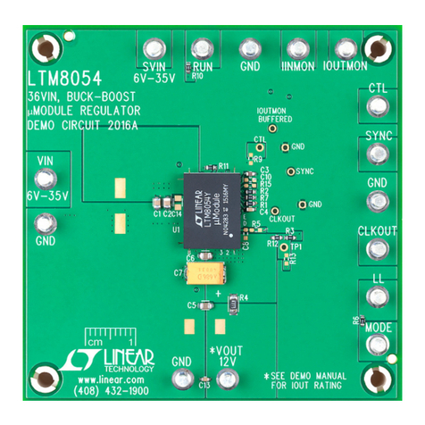
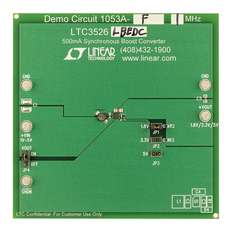
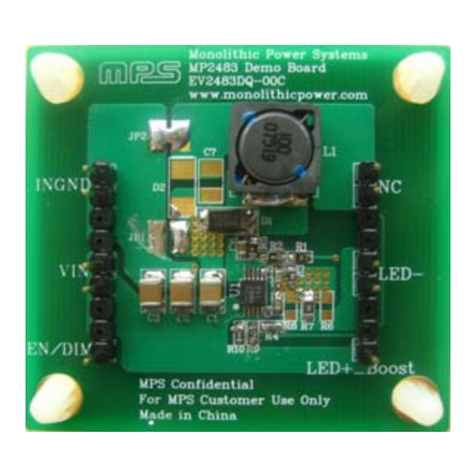
Demonstration circuit 397 is a multipurpose DC/DC
switching regulator using the LT1930A and LT1931A, the
industry’s fastest and highest power voltage regulator in
a SOT-23 package. The demo board offers three sepa-
rate DC/DC converters for different applications needs.
The boost circuit is designed to convert a 5V input to
12V output at 250mA maximum load. The SEPIC circuit
generates a constant 12V/250mA (max load) output with
a 10V~16V variable input. The inverter circuit is de-
signed for applications requiring negative 12V/250mA
(max load) from a positive 12V input. All three circuits
are designed to demonstrate fast switching frequency
(2.2Mhz), an internal 36V/1A switch, wide input range,
and small circuit size. These circuits are designed for
space-conscious low profile applications such as cellular
phones, palm top computers, digital cameras, and LCD
displays. The 2.2MHz switching frequency, 1A integrated
switch, small circuit size, and low component count
makes the LT1930A and LT1931A also suitable for PC
cards, miniature disk drives, xDSL power supplies, flash
memory products, and local 5V or 12V supplies.
Design files for this circuit board are available. Call
the LTC factory.
QUICK START PROCEDURE
Demonstration circuit 397 is easy to set up to evaluate
the performance of the LT1930A and LT1931A. Refer to
Figure 1, Figure 2 and Figure 3 for proper measurement
equipment setup and follow the procedures below:
NOTE:
When measuring the output ripple, see Figure 4
for proper scope probe technique.
The equipment setup for the three circuits is very simi-
lar. They all have three pins marked “Vin,” “Gnd”, “Vout”
and a jumper marked “on” and “off” for demonstrating
the shutdown function.
BOOST CIRCUIT (LEFT SIDE OF BOARD)
1.
Before turning on the power, connect a 5V, 1A bench
supply to the Vin and Gnd terminals and connect the
output loads (up to 250mA).
When an electronic load is used, connect the load
AFTER turning on the input supply and the output
voltage has stabilized.
Connect the oscilloscope and meters to the Vout and
Gnd terminals, as shown in Figure 1. For the best ac-
curacy it is important to connect true RMS reading
voltmeters directly to the PCB terminals where the in-
put and output voltage are connected. True RMS read-
ing ammeters should be used for current measure-
ments.
2.
Turn on the input power supply and observe the out-
put. The DC397 boost circuit is programmed to gen-
erate 12V from a 5V input. The circuit will deliver up
to 250mA at 12V.
3.
With the 250mA load at the output observe the
switching frequency ripple at the output using the os-
cilloscope. The typical switching frequency is around
2.2MHz. See Figure 4 for proper measurement tech-
nique.
4.
The current limit is tested by increasing the load past
300mA. The current limit will take effect when the
peak switch current becomes higher than ~1A. When
the current limit is exceeded, the output voltage will
drop drastically. Return to normal operation by re-
moving the load.
5.
The SHUTDOWN function is tested by placing the
jumper in the off position. This will short the shut-
down pin to ground and turn off the internal switch of
the LT1930A. Placing the jumper in the on position
will return the circuit to normal operation.
SEPIC CIRCUIT (MIDDLE OF BOARD)
1.
Before turning on the power, connect a 16V, 1A bench
supply to the Vin and Gnd terminals and connect the
output load (up to 250mA).
1

