Linear Technology DC2261A User manual

1
dc2261af
DEMO MANUAL DC2261A
Description
High Side Current Sense
with Comparators and a
400mV Reference
Demonstration circuit 2193A features the LT
®
6119, a
high side current sense amplifier with comparators and
a 400mV reference.
The demo board circuit amplifies the voltage across an
onboard current sense resistor, to provide a precision
unipolar voltage output that is proportional to the sensed
current.Theboardhastwoonboardcomparatorswithlatch-
ing outputs and an integrated 400mV reference that sets
the threshold for the comparators. There are two versions
of the board, A and B. The version determines the available
comparator inputs. The DC2261A-A (LT6119-1) has an
inverting and a noninverting comparator input available
while the DC2261A-B (LT6119-2) has two inverting inputs
L, LT, LTC, LTM, Linear Technology and the Linear logo are registered trademarks of Linear
Technology Corporation. All other trademarks are the property of their respective owners.
performance summary
available. The demonstration board includes circuitry to
guarantee that the comparator resets on power up. The
current sense gain and current fault limits are set by on
board resistors. The default gain is set at 10V/A and the
comparators are set to trip at current thresholds of 50mA
and 300mA.
The key performance specifications are listed in the table
below.
Design files for this circuit board are available at
http://www.linear.com/demo/DC2261A
Specifications are at TA= 25°C
SYMBOL PARAMETER CONDITIONS MIN TYP MAX UNITS
VIN Input Supply Range 2.7 60 V
VOUTA Measured Output Signal ILOAD = 100mA 1 V
ILOAD Output Load Current Range Thermal Limit of RSENSE 3 A
IQIN Quiescent Current VIN = 12V 600 µA
ITHR1 Comparator1 Threshold VOUTA = 3V 300 mA
ITHR2 Comparator2 Threshold VOUTA = 0.5V 50 mA
operating principles
TheLT6119 operates byamplifying the voltagedrop across
a sense resistor that is in series with the load. The sense
inputs of the amplifier differentially measure the sense
resistor voltage drop to control an internal variable current
source that allows translation of the input voltage level to
a level referenced to the GND. The circuit gain is set by
the ratio of the output resistor to the input resistor. The
comparator thresholds are set by the internal reference
and the current trip points are set by dividing the output
resistance into a network of three resistors. The RC filter
connected to the latch enable (LE) pin guarantee that the
latch enable pin is held low long enough on start-up to
reset the comparator output on power on.
The DC2261A is shipped with a 100mΩ sense resistor.
The amplifier gain is configured for 100V/V, providing an
overall circuit gain of 10V/A. The current fault thresholds
are set at 50mA and 300mA.
2
dc2261af
DEMO MANUAL DC2261A
Block Diagram
100Ω
OUTA
–
+
–
+
9
10
18
INC2 7
INC1 6
V+
V–
V–
V–
V–
V+
3k
V+
3k
SENSEHI
SENSELO
100nA
UNDERCURRENT FLAG
OVERCURRENT FLAG
2LE
3OUTC2
4OUTC1
34V 6V
–
+
V–
V+
5
400mV
REFERENCE
100Ω
OUTA
–
+
–
+
9
10
18
INC2 7
INC1 6
V+
V–
V–
V–
V+
3k
V+
3k
SENSEHI
SENSELO
100nA
OVERCURRENT FLAG
OVERCURRENT FLAG
2LE
3OUTC2
4OUTC1
34V 6V
–
+
V–
V+
5
400mV
REFERENCE
V–
LT6119-1
LT6119-2

3
dc2261af
DEMO MANUAL DC2261A
Quick start proceDure
With the demonstration circuit, it is easy to set up and
evaluate the performance of the LT6119. Refer to Figure 1
for proper measurement equipment setup and follow the
procedure below:
1. With the power off, connect the power supply positive
to IN and the common to GND. With default settings
the supply can range from 2.7V to 60V. If the supply
does not have an accurate current readout, a DMM may
be connected in series with the supply as shown in
Figure 1.
2. Connect a voltmeter or oscilloscope to the OUTA with
the common input connected to ground.
3. Turn on the power supply. The comparator outputs
start in a known state as shown in the following table
if there is no load attached.
PART OUTC1 OUTC2
DC2261A-A LT6119-1 High Low
DC2261A-B LT6119-2 High High
4. Connect a load to the demo board OUT terminal (posi-
tive) and ground. The load may be a power resistor,
active load instrument or a circuit of interest.
5. Measure the output voltage and confirm that it corre-
sponds to the load current. VOUTA (V) = 10 • ILOAD(A)
for the factory installed resistors.
6. If able, sweep load current from 0A to 300mA to verify
the operation of the comparators. Use the reset push
button to reset latched comparator outputs.
Figure 1. Test Setup
200Ω

4
dc2261af
DEMO MANUAL DC2261A
current sense gain
The gain of the LT6119 current sense amplifier is set by
the ratio of ROUT and RIN resistors. In the demo circuit
this means that the gain is set by the ratio of (ROUT)/R4,
where ROUT = (R7 + R10 + R11) || R8(OPT). The default
values are R7 = 2k, R10 = 6.65k, R11 = 1.33k, and R8 is not
installed. This provides a gain of 9.98k/100. By installing
the optional resistor, R8, the gain can be reduced. The gain
error is primarily set by the precision of the resistors used:
The provided resistors are a 1% tolerance which will
dominate the gain error. To reduce system gain error, the
resistors can be replaced with 0.1% resistors.
Jumper Summary
JP1: The Logic supply jumper has two settings.
- V+: the comparator output is tied to the V+supply
- EXT: the comparator output is tied to an external
supply on the VLOGIC Turret
Optional Settings
1. To power the LT6119 from a supply separate from the
load, remove R1 and connect the power supply to the
V+turret.
2. There are a number of optional components that allow
the DC2193 to be tailored to a specific application:
A) To free comparator inputs INC1 and INC2 for other
use, remove R7, R10 and R11 and install R8. Con-
nect LE turret as required.
B) To add filtering to the amplifier output, install C3.
C) If driving the LE turret from an external source,
pressing the reset button, SW1 will short the signal.
A resistor can be added at R13 to help isolate the
external signal.

5
dc2261af
DEMO MANUAL DC2261A
Information furnished by Linear Technology Corporation is believed to be accurate and reliable.
However, no responsibility is assumed for its use. Linear Technology Corporation makes no representa-
tion that the interconnection of its circuits as described herein will not infringe on existing patent rights.
schematic Diagram
5
5
4
4
3
3
2
2
1
1
D D
C C
B B
A A
TECHNOLOGY
TECHNOLOGY
TECHNOLOGY

6
dc2261af
DEMO MANUAL DC2261A
Linear Technology Corporation
1630 McCarthy Blvd., Milpitas, CA 95035-7417
(408) 432-1900 ●FAX: (408) 434-0507 ●www.linear.com
LINEAR TECHNOLOGY CORPORATION 2015
LT 0115 • PRINTED IN USA
DEMONSTRATION BOARD IMPORTANT NOTICE
Linear Technology Corporation (LT C ) provides the enclosed product(s) under the following AS IS conditions:
This demonstration board (DEMO BOARD) kit being sold or provided by Linear Technology is intended for use for ENGINEERING DEVELOPMENT
OR EVALUATION PURPOSES ONLY and is not provided by LT C for commercial use. As such, the DEMO BOARD herein may not be complete
in terms of required design-, marketing-, and/or manufacturing-related protective considerations, including but not limited to product safety
measures typically found in finished commercial goods. As a prototype, this product does not fall within the scope of the European Union
directive on electromagnetic compatibility and therefore may or may not meet the technical requirements of the directive, or other regulations.
If this evaluation kit does not meet the specifications recited in the DEMO BOARD manual the kit may be returned within 30 days from the date
of delivery for a full refund. THE FOREGOING WARRANTY IS THE EXCLUSIVE WARRANTY MADE BY THE SELLER TO BUYER AND IS IN LIEU
OF ALL OTHER WARRANTIES, EXPRESSED, IMPLIED, OR STATUTORY, INCLUDING ANY WARRANTY OF MERCHANTABILITY OR FITNESS
FOR ANY PARTICULAR PURPOSE. EXCEPT TO THE EXTENT OF THIS INDEMNITY, NEITHER PARTY SHALL BE LIABLE TO THE OTHER FOR
ANY INDIRECT, SPECIAL, INCIDENTAL, OR CONSEQUENTIAL DAMAGES.
The user assumes all responsibility and liability for proper and safe handling of the goods. Further, the user releases LT C from all claims
arising from the handling or use of the goods. Due to the open construction of the product, it is the user’s responsibility to take any and all
appropriate precautions with regard to electrostatic discharge. Also be aware that the products herein may not be regulatory compliant or
agency certified (FCC, UL, CE, etc.).
No License is granted under any patent right or other intellectual property whatsoever. LT C assumes no liability for applications assistance,
customer product design, software performance, or infringement of patents or any other intellectual property rights of any kind.
LT C currently services a variety of customers for products around the world, and therefore this transaction is not exclusive.
Please read the DEMO BOARD manual prior to handling the product. Persons handling this product must have electronics training and
observe good laboratory practice standards. Common sense is encouraged.
This notice contains important safety information about temperatures and voltages. For further safety concerns, please contact a LT C applica-
tion engineer.
Mailing Address:
Linear Technology
1630 McCarthy Blvd.
Milpitas, CA 95035
Copyright © 2004, Linear Technology Corporation
This manual suits for next models
2
Table of contents
Other Linear Technology Temperature Controllers manuals

Linear Technology
Linear Technology LTC2997 Quick setup guide

Linear Technology
Linear Technology DC2258A User manual

Linear Technology
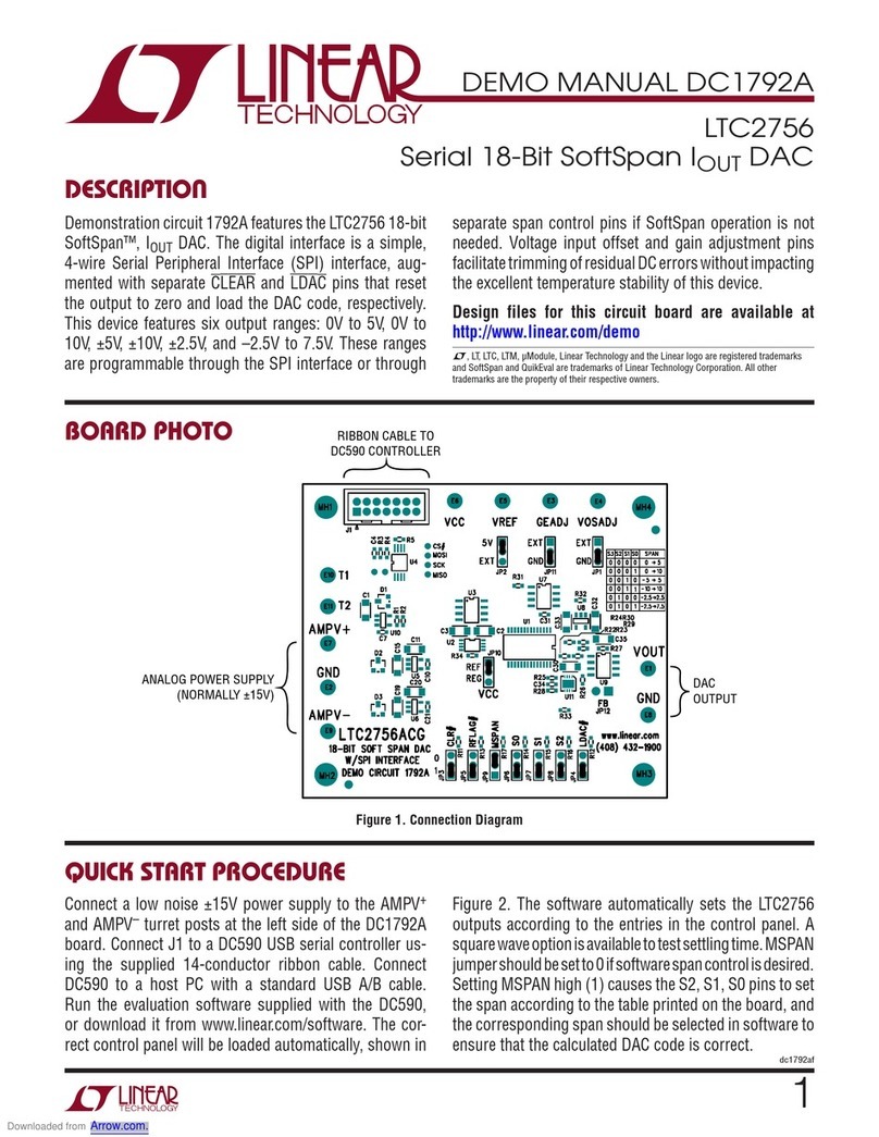
Linear Technology DC1792A User manual

Linear Technology
Linear Technology LTC4361 User manual

Linear Technology
Linear Technology LTC 4362 User manual

Linear Technology
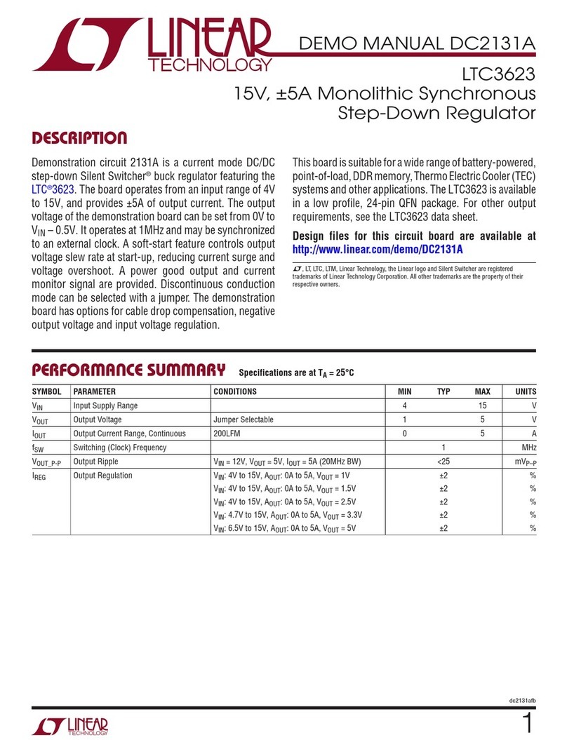
Linear Technology DC2131A Quick setup guide

Linear Technology
Linear Technology DC1871A Quick setup guide

Linear Technology
Linear Technology DC1861A User manual