D E S C R IP T IO N
Demonstration Circuit 1304A features tw o programmable
filter ICs, the LTC660 dual, matched, bandpass filter and
the LTC6603, dual, matched, low pass filter.
The DC1304A
The DC1304AThe DC1304A
The DC1304A-
--
-A
AA
A is for
is for is for
is for an LTC660 and
an LTC660 and an LTC660 and
an LTC660 and
The DC1304A
The DC1304AThe DC1304A
The DC1304A-
--
-B is for
B is forB is for
B is for an LTC6603.
an LTC6603. an LTC6603.
an LTC6603.
The LTC® 660 is a dual, programmable bandpass filter
and differential driver. The selectivity of the LTC660 is
ideal for filtering baseband tag signals in RFID systems.
The LTC® 6603 is a dual, programmable low pass filter for
communications receivers and transmitters in TD-SCDM A,
W CDM A, CDM A 000, UM TS and 80 .11x systems. A
DC1304A-A or ---B board has tw o pairs of SM A connectors
for differential inputs and tw o pairs of SM A connectors for
differential outputs. The differential inputs can be AC cou-
pled or DC coupled. O n board jumpers provide control of an
LTC660 or an LTC6603. The jumper control settings are:
serial or parallel control, internal or external clock, gain and
bandw idth control and input AC or DC coupling. An on
board multi-turn potentiometer sets the value of the R BIAS
resistor that sets the IC pow er supply current and clock
frequency. PCB turrets provide for board connections to an
SPI master for a serial control of IC gain and bandw idth.
LTC660 features:
LTC660 features:LTC660 features:
LTC660 features:
Guaranteed Phase and Gain M atching Specs
Programmable 5th Order Low pass: 40 kH z to 900 kHz
Programmable 4th Order Highpass: 4 kHz to 90 kH z
Programmable G ain (0dB/1 dB/ 4dB/30dB)
Simple Pin Programming or SPI Interface
Input R ange Extends from 0V to 5V
Low Voltage O peration: .7V to 3.6V
Shutdow n and M ute M ode
4mm × 4mm Q FN Package
LTC6603 features:
LTC6603 features:LTC6603 features:
LTC6603 features:
Guaranteed Phase and Gain M atching Specs
Programmable 9th Order Low pass: 4 kHz to .5 M Hz
Programmable G ain (0dB/6dB/1 dB/ 4dB)
Simple Pin Programming or SPI Interface
Input R ange Extends from 0V to 5V
Low Voltage O peration: .7V to 3.6V
Shutdow n M ode
4mm × 4mm Q FN Package
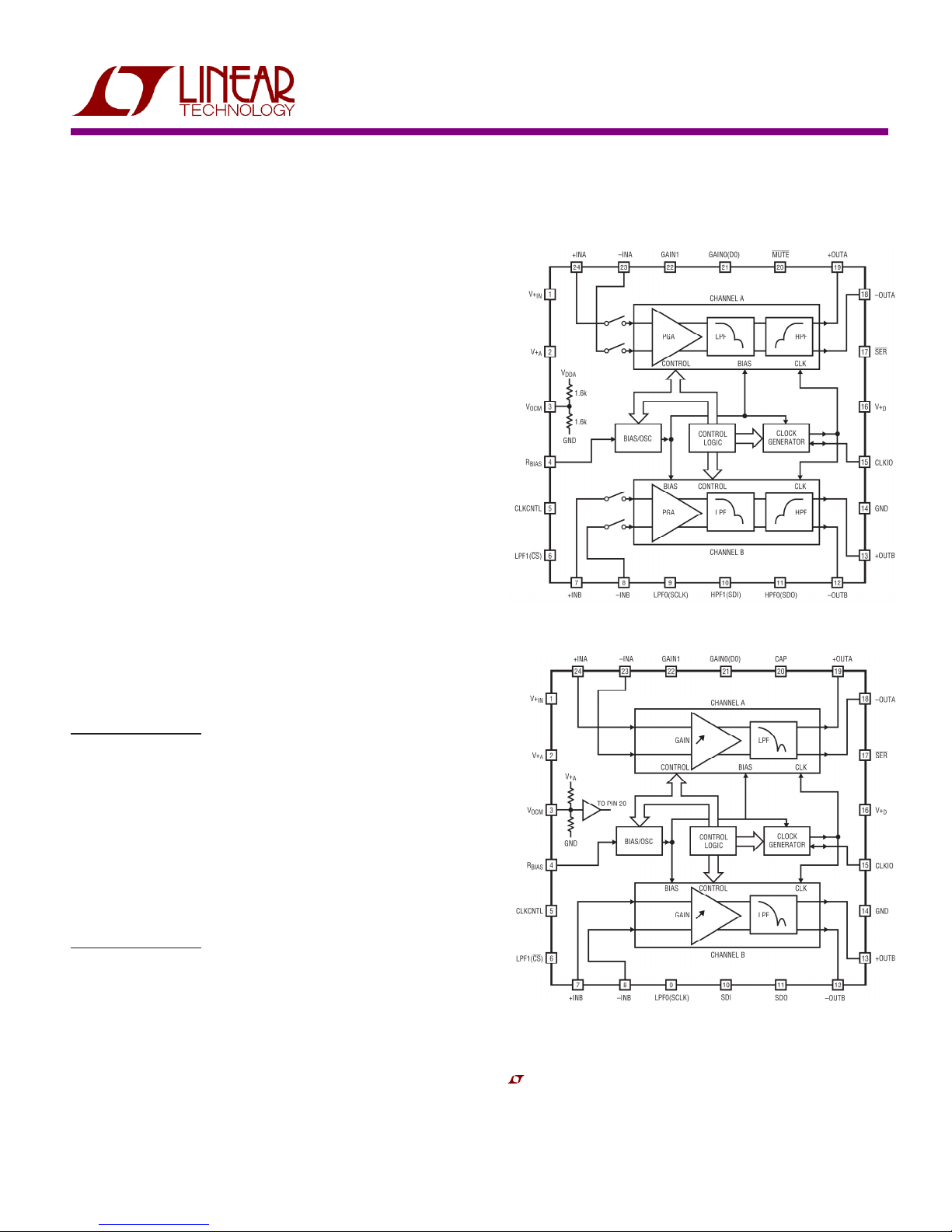
T h e L T C 6 6 0 2 B L O C K D IA G
T h e L T C 6 6 0 2 B L O C K D IA GT h e L T C 6 6 0 2 B L O C K D IA G
T h e L T C 6 6 0 2 B L O C K D IA G R
RR
RA RA M
A RA MA RA M
A RA M
T h e L T C 6 6 0 3 B L O C K D IA
T h e L T C 6 6 0 3 B L O C K D IAT h e L T C 6 6 0 3 B L O C K D IA
T h e L T C 6 6 0 3 B L O C K D IA R
RR
RG A RA M
G A RA MG A RA M
G A RA M
Design Files for this circuit are available.
Design Files for this circuit are available.Design Files for this circuit are available.
Design Files for this circuit are available.
Call the LTC factory.
Call the LTC factory.Call the LTC factory.
Call the LTC factory.
, LTC and LT are registered trademarks of Linear Technology Corporation.
L T C 6 6 0 2 / L T C 6 6 0 3
P RO G RA M A B L E B A N D P A S S / L O W P A S S F IL T E R
D E M O C IRC U IT
D E M O C IRC U IT D E M O C IRC U IT
D E M O C IRC U IT
1 3 0 4
1 3 0 41 3 0 4
1 3 0 4
Q U IC K S TA RT G
Q U IC K S TA RT GQ U IC K S TA RT G
Q U IC K S TA RT G


