LPB AM-30P Series User manual

AM-30P Series
AM
Transmitter
Manual
Model: AM-30P
LPB COMMUNICATIONS, INC.
311
Spruce Street
Camden,
NJ
08103-1929
856 365-8585
PH
856 365-8999 FX
www.lpbinc.com
From the library of WØMTU

CAR.R[ER
CURRENT
2.nd
RA.DlATr~G
Cp.8LE
SYSTEMS
TABLE
OF
CONTENTS
Section Description page
1.0 INTRODUCTION
2.0 WARP-ANTY AND SERVICE 1
71
Limited Warranty
2.2 Service
3.0 APPLICABLE FCC RULES 2
40
CIRCUIT DESCRIPTION 2
4.1
Summary
4.2 Power Supply
4.3 Exciter
4.3.1 Audio
4.3.2 Oscillator
4.3.3 RF Pre-Driver and Driver Stages
4.4 RF Power Amplifier
4.5 Audio Limiter (-L Option)
5.0 INSTALLATION 5
5.1
Location and Mounting
5.2 Interfacing the Transmitter
6.0 CONTROL SETTINGS AND OPERATION 5
6.1
User Control Description and Location
r
.......
,
CL
Se~up
and
Oper2~i(F!
From the library of WØMTU

-
!~,
-
.-
-
,.-
.-,
.--...
.•
--
I
...........
.-
-'
--
-
'.~
-
.=
-=
::-
-
.....
,;
~'
\-
:;.
,-..
7
INSTRUCTION
MANUAL
LPB
l\10DEL Al\1-30P TRANSl\1ITTER
CARRIER CURRENT and RADIATING
CABLE
SYSTEMS
Revised
MAY
2006
1.0
INTRODUCTION
Low
Power
AM Transmitters are the product
of
LPB'
s nationally recognized broadcast experience since
1960- This P version solid state transmitters utilizes state-of-the-art technology and has been Type
Approved for licensed use under Part
73
of
the
FCC
Rules
and Regulations.
The
transmitter
power
output
(TPO)
is
adjustable
down
to about 2 watts. This freedom allows greater flexibility
of
system design,
2.0
Warranty
and
Service
Information
2.1
Limited
Warranty
We
guarantee that you will find the appearance, \vorkmanship and standards
of
material and construction
of
this equipment in keeping with the application and ,vith good standards
of
commercial practice.
For
a period
of
one year from date
of
delivery.
we
guarantee this equipment against any form
of
failure
provided that, m the opinion
of
the manufacturer, no
improper
use
of
or modification to this equipment
is
at
fault. The guarantee also requires tbat the equipment IS properly instalied and operated within stated
parameters During this period, LPB will fumish materials and labor in
our
shops to
coneet
any failure.
Shippll1g charges are the responsibdity
of
the customer, After walTanty explrati0l1. service will continue
to
be available from LPB.
Pagei
From the library of WØMTU

,~.
"
.
~
.
",
.
"."-"
. .
.-'
-
.-
~
~
.....
.'::
~"
"
.
,.
.
....
-
....
-
~,
, -
~
C;1je~:~:c,~~
SllC:~J.L:
ai-:Se.
;=":je2.s"~
':'311
:!r
\\";-i',::-
LPE
C'LS'\'='~111er
Ser\'i:e
i:::..iTi::"cldL"eiy
IC:~lrl~i)"=(;llC:ll
ird"~:-::~".c"i.ic..n
'\\"hiCb
"
;:"IL!
shcy~ld
~~.r0·'
..
ioe
·.i,:he:J
:z,iiing
0;'
\~I";'i':;Eg
1:'1C~JJeS,
n~c)df!
il;,.E:lbe~'
ser~zj
j-ll.L1J~!ei·.
::pe~·3~i~:g
fi'e~u::~!c~\
2l-J"j
8~ll':"
,::)f
pl.l:"cllaSe,
TbJS
1Il~'oL~rl3~10:1
Is
found
011
rile
]denlitlc2~jon
13~ej
,~r;
L~le
T;-ans;"11i7~e:'
This
equipment,
in
general
IS ?\OT
CSER
SERVICEABLE.
If
a
m~.lfuDction
arises
or
is
suspected,
\ve
urge
~ou
to r-eturn
the
equipment
to
the
factor~'
for
proper
repair.
If
the
need
for
service
arises
contact
LPB's
Customer
Service
Department
for
a
Material
Retum
Authorization
(l\:IRA)
and
shipping
instructions
before
shipment.
The
l\1R--'\.
number
must
appear
OIl
the
shipping
label.
LPB
Communications,
Inc.
Phone
856-365-8585 Fax
856-365-8999
3.0
APPLICABLE
FCC
RULES
-\\1ARNING!!!!
In
paragraph
10
of
Report
and
Order
in
the matter
ofMM
Docket 85-125 adopted December 20, 1985,
the commission amended Pari 73.58 to read as follows:
"
However,
auxiliary transmitters \vith nominal
power
ratings
of
100 watts
or
less
are
not required to
be
equipped
with instruments to determine
power
by
the indirect
method
provided that the licensee can
determine
t11e
antenna input
power
at all times."
The
Relative
Power
Output meter in the LPB
AM-30P
transmitter
does
not satisfy this
metering
requirement.
We
suggest the licensee
employ
an
Antenna Current Meter,
such
as
the
Simpson
model
37 (
3
Y2
)RF Ammeter. When looking into a 50 ohm load, the 30-watt transmitter needs a
0-1/\
full-scale
ammeter.
It should
be
noted that the
Commission
does not require the RF
ammeter
meter
to be m the circuit
a1
alJ
times, however, you must have and
use
this capability to
measure
the output.
3.1 ADVISING
THE
FCC
When
installing a
transmitter
for use with low
power
authorization, the user must
advise
the
Commission,
in writing
of
this action.
The
make and
model
number
of
the transmitter
must
be
submitted.
4.0
CIRCUIT
DESCRIPTION
We
do not recommend user repair
of
this equipment
but
furnish the following theory
of
operation
information for those interested. It will assist in isolating a problem. Furthennore, refer to the
troubleshooting
guide in Section 7.0
and
to the block
diagrams
and schematics in this manual,
4.1
Summary
(REFER
TO
TRANSMITTER
BLOCK
DIAGRAM,
FIG. lJ
The
transmitter uses an integrated circuit technique to generate a high-stability signal at six times
the
carrier frequency. A digital countdov,'n circuit produces the carrier frequency. which is tben
amplitude
modulated
at
a low level. A
linear
RF
power
amplifier increases the output to full rated TPO.
The
linear
RF
amplifier
allows output
power
adjustment down to about 10%
of
rated
TPO.
The internal
meter
is
used to
measure
Modulation and
Relative
RF
Power
Output.
Page
2
From the library of WØMTU
~:;
-~.
-'-.
c.
j
~';e
ICI\:\ '\'oitage
5'e"::0nja:~\'
(',"
;~:\..:\\·el-
:;'2~~~-:-0~1~-!;::;"
:T:'
{E':'c.~
c:
s;.2:'!d:,;-d
f~d-",7\Z;\t
c;!~}d~
8rjcg·~
(CR~!
Dl·:·,je
C.R,2
and
:rans;stor
Q~
j)~~C"=,·f.~e
;'e~~t;(-I·.iO!j
a~lC
:"i~)rle
:-=.ie.c;il,,~)~-.i..
CR3
pro\"lcles
j~all-\\'3\:e
j"c,::inc21.Ion
i'or
tbe 1
~\"DC
s-~lppl).
3cJ:h
P;'lI1121~\
'!-
....
C:
ai~lc
G-
\ ol:sges
2~'e
fused (Fl &
F.2)
..
~
111clal
o\Jde
\'arisl:ol
'/I
shunts tbe
tov\:
\"oltage
secondci!~\:
of
1~}
to
p;'0tect aga:nst danlage
fr0~11
voltage
transients~
4.3
Exciter
(Refer to Exciter Fig. 3 and
sC~1emaiic)
(PariS
Lis, =60
lC-FJ
4.3.1 .-\udio
The
audio section utilizes mput
transfonner
T2 to provide isolation and
balanced
600
OlUl1
line
Input
The
transfonner
secondary
drives operational amplifier A 1
in
the inverting
mode
This feeds an integrated
circuit balanced
modulator
A4
and the input
of
the
meIer amplifier A6.
The
meter
is calibrated to indicate
o
VU
at 100%
modulation
with a tone input
[]
kHz
standard) connected to the transmitter
audio
input.
Balanced
modulation
A4 provides a low level amplitude modulated signal. This output is
square
wave,
rich in harmonics.
DC
voltage for the audio input stage, meter amplifier and
modulator
is
provided from a
sub-regulated
power
supply for high stability.
4.3.2
Oscillator
A
precision
crystal is used in the integrated circuit oscillator A2.
It
operates
at six times
(he
lransmitter
carrier
frequency for
maximum
stability. The oscillator output drives- a divide-by-six
counter
A3, This
output
is
square
wave
at
the
carrier
frequency
and
is applied
10
the
modulator
A4.
.---
__
-Ir{1
Ii
I\/ID
E
BY
SL\
!_~
,I
COUHiER
I
r:"Y
"'T
..
AL
vK,'::>
OSCILLATOR
I
AUDIO
AMPLIFIER
I
')1
(~"
I
AUDIO
")
I (
2,/
.
f-01E
TE
R I
f\
"'."('. FIL
TER
-------(il{Ir"""_
. , ,
__
~.-,
'J
'
n~PUT
<~
II
~
/<;-
~IFIER
I
"J
I
.......
I
/--"
i
\/1
I \
'-----I'--
\ .
~
I
.......
~-------"
RF
OUTPUT
TRA
I\J
~~~
Ivi
ITTE
k'
" /
FIG, 1
Page3
HOTIULATOR
DETECTOr:;:
DRIVER
PD\JER
Ar~PLrF
IER
From the library of WØMTU

C3
E
11)
+28
[.©r
-- !
ul
PO\,VER
SUPPLY
Component Layout
From the library of WØMTU

--------
~----ll
1---1
C1
L,
T I
V-l
II
I
I
Ql
I
I I
L. J
~_l
I
T1vr
r
R2
~
~
I
CR21
C3 L+
NVV'-.
)
CR3
f -
l
__
~-I~
Fl
~
JRI}
~~
II
1+28
v.
I-------------r--I
:D
3
DSl
Sl
~
'-------------8
1+
15
v,
·--·--I~~~
--~---o
1
(j--
/
0'------
----:~:::~::--
---~
I
_L
ASS'Y
#
6015
REV.B
L~
·
__
J
.A}!I-t30P/60P/100P
POWE_R
SU.PPLY
~/J6016
REl'V.13
From the library of WØMTU

~mTE1
RESIS:CR R14
IS
~·1DUNTED
ON
BACK
OF
BOARD,
AUDIO
INPUT
AUDIO
GAIN
GND
+15
o
DET
GND
SEE
NOTE
112
GND
RF
RF
OUT
DRIVE
~1DTE
#1:
U IS F
ACTDRY
ADJUSTED
NOTE
#2; C43
IS
FACTORY
SELECTED
FIG,
3
AH-30
P
EXCITER
From the library of WØMTU

---
C24 R37
~l-O
I
11---
R32
R30
R47-L
-=
--
-
+~17
R17
R25 2
8
A4
~
R24
-=
CIG"
+
C20
> > > -I ,
_
L+
J J I
CBI
1'--'---
--1
R14
ell
FREGl
S R26
.:I:
-
~
POINT
R19
-
lfu~7C~-=
1
IE.
11
.:
'-
TEST
C -
,-
8
2 I
10
R27
A3
I
A2
R16
[ 3
14
5_
6
-
..
' •
.-----,
-,
j
Rll
-
10
-
8LyJ9
I I
ITC47
_
o-l
ID~l
-
R9
... R22 > , - -
+
';REGl.
TRII'I
~
~
~
L6
0--
C5
)
+
-=
·
T2
C6
-
R33 +15V
cr1R4
10
R10
-0
:;nII
C
~UDID
T 6
,
AUDIO
::-u
~
~
GAIN
R51
TEST
IN
REL
/.
•
R7
I
-
AUDIO
-.
-=R6 -R52
POINT
IR
RF
2 0 .
[JUT
RF
OUT
MOD
I D8 _ 9
C9
4 • I
1
R12
I·
R36
-:-
1
->
R541
-
-
i
_._J
1-
,.
__
._.
NOTESI
,
p'
VERSION
1.
R12,
R28
J
R55
o.re
fo.ctory
set.
EXCITER
BOARD
SCHEMATIC
2,
REFER
TO
PARTS
LIST
# 6010
Rf
V.
F
AM-30P/60P/100P
FOR
CO~rLE1E
LIST
OF
EXCITER
CQMPDN~NTS
DWG.
6094
REV.
F
From the library of WØMTU

·. .
,"j
-;..-
. .
~,
......
;~
....
::
~.~-]\
'::~
~~-!::
~"';;'::-::-i',":'r
'::"~~''-'
',';:.~'
:l·2ri:::j;lc..~'!·
(~~3
c\pe';~~llij!g
Clas~
,:-~
-;"~;t
?'-~
,j:-'
\~.
,::-\
t::
'~'=-<-~'.;':=-.~
?~~
j
::-,
~~-Ie
;""~-c-cr;
\
~~
1JSTS.
~Lle
O~ltpU~
;)~'-\.
~~-
:J['t->e
Z:-2:1S;1~:~Ter
l-h;::
GriYer'2':~p:iff'''
;J:-.:
....
.
=;~'.~
;'~.<:"-
...
II""
:;'C
·::~C.;
j)C'
".e·:'
2;~~)
:.-jer
4.4
RF
Power
Amplifier
(Refer to RF
Amplifier
Fig. 4 and schematic) (Parts LIs; S 600.5-A]
Tbe fimJ pO\l\er
amplifier
utilizes a
matched
pair
of
baianc:d
en~itter
transisto,'s Q5 and Q6. Bias must
tJe
supplied for linear
/v\1
amplification. This operating bias is de\'eloped
111
a
senes
regulated bias supply
whose main
conlponents
are A5 and Q4, Because
,be
po"
er
3iTlpiifier
is
push-pull and the transistors are
matched, a high
degree
of
second harmonic rejection
is
automallcally achieved
..
\11
elliptic function filter
(C31 thru C35, L4 & L5)
at
the
power
amplifier output rejects higher order harmonics. Transmitter RF
output is sampled to present Relative
RF
Output on the
VU
meter
with tbe switch (S2),
011
the exciter,
in
the REL RF
OUT
position.
The
elliptic filter is designed to operate over one-third (1/3)
of
the
530
kHz to 1710
kHz
AM
band.
Sectioning the
band
with
different filters is necessary
because
of
the
width
of
the band.
For
example; the
second
harmonic
of
530 kHz falls
within
the band at 1060 kHz, and the third
harmonic
at 1590 kHz is
also
within
the band.
The
low-band filter covers 530
kHz
to 830 kHz, mid-band 840 kHz to 1270 kHz and
high-band 1280 kHz to
1710kHz.
Any field
change
of
frequency will
be
restricted to the
operating
range
of
the filter.
For
example: a 640
kHz
transmitter
can
be
changed
to operate on
710kHz
by simply
changing
the crystal,
but
it cannot be
operated
above
830
kHz
without first
bel11g
retumed to tbe factory for a new elliptic output filter and
adjustment
of
the
power
amplifier.
Page 4
From the library of WØMTU

--
r-------
---I
I T4 B
L5
L4
O
~_~LJT
o
----r--r-...-..l
I
'vi
,
~~]~1l
:~
~~
I
C31)
IC36
lR45
~
L2
L3
+28
cr----·
, +
C26
-'-'
-'-
C27
I I
C29
I
-
+15
R46
INI
lou~
0-------- ,
J\/\/\/'
, I A5
C38
~
C37
+~
R40 <
~<
R39
II 7 +
-L
r----l\
I <
R38
l.
_
AM-30P
160P
1100P
RF
PO~ER
AMP
MODULE
RFA-30
SCHEMATIC
Dwg,
No,
6006
REV,
A
Q6
From the library of WØMTU

:
......
..
=;.
",
.-
:-~-"
-~.-
.-
-:-
.-.
-=:7--
__
.'
-~.
._1
-..'._.
-'--'
i
i
~!
,;
i
~.
i •
,:
i
....
,; j : 4
-,--
"-
-'
·-····-·7 '---J
"-'
..::...
-'-:
-,--:
i
."-"
-1.
-:
--
'--
__
'--i
"-"
..
_'
'_.'
; i
..
;-:.:.
"
~:
.~-----
-,
'-.
;~
j r
--;--------;
:i
I,
~
i ;
L4
i
'.J
I 2 iI
~
~
l_
-t--+
,tl--~
Ii-~
..
-<
r~:~:",
f!
If
,.'"
.
I"
.-';---
.
.'
...
1""./)
l
/
r-;""
r-',p"
"r
II
I
.~'-
(11~~CJ~/!
i~
,
r{:';?yj
04
I
i':{~:~l
iI I
L+th
.
I.
:
I
R4-1
I
I
I
I
1
I
I
I
,
I I
i
II
ii
I
I
_.-
,,'
RF
POWER
AMP
COM
P 0 N E N T L A YO U T FIG, 4
From the library of WØMTU

II
I
83/16'
11
7/fj-
l
~
2
3/8'
l
~
31/2"
~
31/2"
-
37/64-
<,<'l_
11
5:0
1
I
TRANSM[TIER
t..10UNTING
DIMENSIONS
FIG.7
y=
==~
II
II
Ii
!'~--"\
..
,
...
-\
'-;'.;.,
II
!
'.
I
""
./
P,F
OUT
.---...
"_0"
i
II
j r ii
II
I[ I
TR.~
I'~
S
~,.~
ITIE
R
I OUTLINE &
f,iOUIHII~G
I
VIEWED
FROM
FRONT
j"
,
I
I
,
PCYv\/ER
CORD
CHASSIS \/IEWED
FROt-.1
BOnOM
TPANS~,~I-I
FIG.8
IER CONNECTIONS
From the library of WØMTU

·
..
.
'll"ie
\
'~:-1~
;ICl
e;
2l1G
"Lhe
air
circula:;·Jl1.
Do
l,CJ[
;,lOUDt
,11e
transminer
to an ('lectnca)}y
conductive
surf8ce. We
recommend
a ',"ooe
OJ
similcH
backboard.
Holes
are pro\'ided
in
the rear
of
the chassis ror thTee (3) screws
to
mO'..lnT the tr8ns'i:1iner to 2 vertical
s\.1rTace.
Scre',\s.
=j
0);
5'8", aj'e supplied. Refer [C! Fig. 7
Tor
proper
rilounting.
5.2
Interfacing
the
Transmittel'
AC
power:
The
transmitter
requires a standard 117 VAC, 50/60
Hz.
outlet A 6 foot, 3
conductor
line
cord
with
3 pin
AC
plug
is supplied,
DO
NOT
REMOVE
GROUND
PIN
FROM
PLUG.
A
UDIO:
The
audio input
impedance
is 600-ohm
transformer
balanced.
Any
input level
between
-15 dBm
and
+15
dBm (0.14 VllliS to 4.3
Vrms)
will
provide
100%
modulation
(with
the
Audio
Gain
control R4
property
set).
Connect
the
audio feed line to the
AUDIO
IN terminal block on the
bottom
of
the
transmitter
chassis.
(see
fig.
8)
RF
Output:
The
RF
output
impedance
is industry-standard 50 ohms,
unbalanced,
using
an
SO-239
UHF
type
connector
(see
Fig, 8).
The
RF
output
cable
must
be
50
ohm
coaxial.
Type
RG-8/U
is
recommended.
For
short runs, type
RG-58/U
is acceptable.
NOTE:
A
strong
RF
field eXIsts
within
a few feet
of
the transmitter and
may
affect
the
operation
of
other
equiplYlent located
in
close
proximity
to the transmitter.
6.0
CONTROL
SETTINGS
AND
OPERATION
6.1
User
Control
Descri.ptions
and
Locati.ons
A
number
of
trim
pots
are located
inside
the transmitter.
Some
are factory set
and
sealed.
Removing
any
of
the
seals will void
the
warranty.
User
adjustable
controls
include:
Pm-ver Switch (Sl) located on
the
pO\:ver
supply board.
The
red
LED
will
be
on v,ihen
power
is applied.
Meter
Switch (S2)
located
below
the
meter
on
the
exciter
board.
This
switch selects the
function
of
the
meter
to indicate
Relative
RF
Power
Output or
Percent
Modulation, [see section 4.3.1 and 4.4)
Audio Gain (R4) located on
the
upper
left
comer
of
the
exciter. This adjusts
the
audio
gain
of
the
transmitter
to
provide
100%
modulation
for any audio input level between -15
dBm
and +
15
dBm.
RF
Drive
(R31) located
lower
center
of
exciter board. This control adjusts
the
RF
drive
to
the
final
power
amplifier
for the desired
RF
output
po:wer between 10% and 100%
of
rated
TPO.
6.2
Setup
and
Operation
Refer
to section 6.1
of
this manuaJ and the
operating
lllstructions located on the
inside
of
the
transmitter
fro;'}t panel. With
power
s\\itch
(S
I)
off
(dov,n position)
make
sure
RF
Dri\'e le'vel (R31) and
Audio
Gain
(R4) are
at
MINIMU1\1 (full counter-clockwise).
1.
Be
sure all connections to and from
the
transmitter are secure,
')
TUlll transmitter
power
switcll on.
Place
.flieter FUllction Switch in the Relative
RF
Output positio;l (REi.
RF
OUT).
P&ge
5
3
From the library of WØMTU

-"-(
,':
~y.......
.,
:":::
J.
Apply program
materi'l.!
(audio source]
to
transrnitter
Set
Meter Function
SWilCll
to
percent
mod:.,lation positio'l
(~;
\10D).
is
Adjust
),xiio
Gaw Control
(R4).
Set
gain
I •
so
that
fneter
reads
no
highe:'
'~han
louoeST
prograiTI
1:1atericl
peaks
NOTE: Modulation can also be set using
an
oscilloscope by connecting the scope probe across the
RF
output. Adjust the Audio Gain (R4)
so
that
the
negative modulation peaks are just begmning
to
pinch off
the carrier, then back
off
RJ4
slightly. At a sholi distance from the transmitter, use any
AM
radio
to
listen
for distortion
and
check the quality
of
the audio. Placing the radio close
to
the transmitter may cause input
overloading
to
the radio
and
result
in
a misleading interpretation
of
signal quality.
7.0
BASIC
TROUBLESHOOTING
GUIDE
PROBLEM POSSIBLE CAUSES
LED power indicator does not light No Power on AC receptacle or FI blown
No fuI: output indication Fuse FI and/or F2 blown.
Drive control
R31
set
to
minimum
Meter switch (S2)
in
% MOD position
RF
output reads off scale when Open
RF
output cable
control (R31)
is
advanced
Fuse (F2) blows after a sholi period
of
Defective QI
Operation
No modulation indication with RF output Audio GAIN control (R4) set
to
minimum
No Audio from source.
Audio distortion heard
on
radio Audio Gain set
to
high.
Receiver
is
to
close
to
transmitter.
8.0 MAINTENAJ\'CE
These transmitters are designed for continuous 24-hour service. Peliodic checks
of
the transmitter and
associated eqUipment are recommended
to
catch any problems that may rise.
Page 6
From the library of WØMTU

Fe!
::.=,.
,.;\'1
~l;:;'
SCi-iSril3l:ics:
1
LPB
PARTS
USTS
Sherf
assembly
-
Assemb!y
l\umbsr
600i-A
Symbol
Qty
Description
Part
#
.<
I
AM-30
F[NAL
ASSEr\~BL
y
6002-A
1 i RF
FRONT
PANEL
521-6034-A
3 2
LATCH
GROMET-NYLON
309-1021
4 2
LATCH
PLUNGER
309-1020
5 1 3'
RG-58A/U
COAX,
W/PL-259
933-1040
6 1
AM-30/60
[NSTRUCTION
SHEET
441-6004-A
73 # 10 X
112"
HEX
HS
SHEET
MTL
SCRE'v\!
301-6412
I
8 2
FORK
LUG,
# 6
STUD
22-18
GA
WIRE
195-1015
RF
POWER
AMPUF~ER
PIN
6005-A
1 1
POWER
AMP
PCB
671-6008
R39
1
TRIM
POT,
1K OHM
775-1080
R40 1 RES. 680 R, 1/2W,
5%
762-2117
R41 1
RES.
4.7
R,
1/2W,
5%
762-2065
R42,43
2
RES.
22
R,
1/2W,
5%
762-2081
C27,29,38
3
CAP
..
i UF,
CER
DiSC
50V
174-2197
C28
1
CAP.
22UF,
RADiAL
63V
20%
172-1067
C30
1
CAP
..
33UF,
MYLAR
100V
10%
175-1091
C37
1
CAP.
470
UF
AL
CAP
AX!AL
50V
172-2153
A5
1
LM317T
(TO-202)
363-1001
010
1
DIODE,
1
N4007
781-1037
Q4
1
TRANSISTOR,2N5190
781-1004
Q5,
Q6
2
PWR
TRANSISTOR,
SO-1407
782-1211
L2,L3,T3
3
FERRITE
TORROIO
.75"
201-1005
Page 7
From the library of WØMTU

~
-,
,.,
-.
-
,-
...,
~\...
:.
'-"-.::;
c.
3[
HEp<TSr!~~(
TO-202 PRESS
Or'~
332-'1005
::;
SCREW', .i-40 X
3/8
PH
PHfUPS
30'1-'1i08
5 0
" SCREW, 6-32 X i
/2
PH
PHlLlPS
301-i212
6 6 LOCKVvASHER, EXT
'#
6 303-1010
!..:
'-'
...
/6 KEPS NUT, 10-24 302-6020
9 4
LOCK
WASHER,
#-
4 302-1004
"11
;,
I MICA INSULATOR 789-1021
12-17
HOOK
UP
WIRE 931-10**
C31
Thru
C35 SEE NOTES
L4, L5 SEE NOTES
NOTES"",
..
1.
USE A THIN COST OF
THERMAL
HEATSINK
COMPUND BETWEEN
COIVIPONENT
AND
HEATSINK.
SCRAPE
PAINT!F
REQUIRED.
2.
52
UH
FERRITE CORE TORRO!DAL -SEE SCD # 184-1005
3.
RF
TORROIDAL
TRANSFORMER INPUT TR!FIAL- SEE SCD #865 1005
4.
RF
TORROfDAL
TRASNFORMER
OUTPUT
-SEE
seD
# 865-1010
5.
QUANTiTY
EQUALS
LENGTH
IN
iNCHES
6.
FILTER
COMPONENT
VALUES VS FREQUENCY
RANGE
--------
LOW
BAN
D -----------------MID
BAN
D----------------------HIGH
BAN
D -------------
C31
3600PF (171-1218) 2400PF (171-1202) 2000PF (171-1197)
7.
C32 1000PF (171-1176) 680PF (171-1164) 200PF (171-1120)
8. C33 5600PF (171-1236) 3600PF (171-1218) 3300PF (171-1215)
9. C34 3300PF (171-1215) 2200PF (171-1200) 750PF (171-1167)
10. C35 2200PF (171-1200) 1500PF (171-1188)
1600PF
(171-1191)
11. L4 9.3UH SCD #184-1032
6.1
UH
SCD #184-1023 5.5UH SCD # 184-1021
12. L5 5.8UH SCD #184-1024 8UH SCD #184-1018 4.0UH SCD # 184-1018
From the library of WØMTU

EXCiTER
BOARD
ASSEMBLY
PIr'J
6815·/\
Symbol
Qty
Description
Part
#
f-Jotes
1 1 PCB, EXCiTER- AM30/60/1
00
671-6013
R3 1 RES. 620 OHM
1/2W,
5%
762-2116
R4,R31 2 TRIMPOT, 10KVT 775-1130
R5,R19,R51 3 RES.
10K
OHM,1/2W, 5% 762-2145
R6,R7,R47, 5 RES.
47K
OHM
1/2W,
5%
762-2161
R53,R54
Ri6,
R17,R22 3 RES. 1K
OHr,,1,
1/2W,
5%
762-2121
R33, R34, 2 RES. 1K OHM 2W,
5%
762-4121 2
R9,R30 2
R·ES.
100K
OHM
1/2W,
5%
762-2169
R'1
O,R11
,R14 5 RES. 100 OHM
1/2W,
5%
763-4097 2(r14)
R21,R24
R12,R55 2 TRIMPOT, 1
KHZ
775-1085 1
R13,R18 2 RES. 1.8K OHM
1/2W,
5%
762-2127
R20,R27 2 RES.
3K
OHM
1/2W,
5%
762-2132
R15,R23 2 RES. 820 OHM
1/2W,
5%
762-2119
R25 1 RES. 47 OHM
1/2W,
5%
762-2089
R26 1 RES. 1.3K OHM
1/2W,
5%
762-2124
R28 1 TRIMPOT, HZ
TMWHEEL
775-1135 1
R29 1 RES. 2.2K OHM
1/2W,
5%
762-2129
R30 1 RES. 300 OHM
1/2W,
5%
762-2108
R35 1 RES. 220K OHM
1/2W
5%
762-2177
R36 1 RES.
50
OHM 5W,
5%
765-1247
R37 1 RES. 3.3 OHM
1/2W,
5%
762-2061
R52 1 RES. 22K, 1/2W,
5%
762-2153
C4,11,12,14
7 CAP
.1
UF CER DISK 50V 174-1254
CiS,
18,21
C22.
C5,C19,
C25 3 CAP .001
UF
CER DISK 1000V 174-1155
2
From the library of WØMTU

C23
i
COI-.JTIt-.JUED
....
Synlbo!
C24
Al,A6
A2
A3
A4
D4
05,6,7,8
D9
T2
L1
L6
2
82
Q2
Q3
XI
3
4
5
6
7
8
9
10
11
12
14
15
i6
1
2
1
1
1
1
4
1
1
1
1
14
1
1
1
1
1
1
1
1
1
3
1
1
2
2
2
2
1
CAP
,33 UF fViYLAR
100V
10%
Descr'iption
CAP
.15 UF
MYLAR
lOOV
10%
IC
RfVi74'lDC
(14
PIN DIP)
IC
MC12061
P ( 16 PIN DIP)
IC
LM7492PC
(14
PIN DIP)
IC
MC1496P
(14
PIN
DIP)
DIODE
1
N4742A-12V
DIODE,
ZENER
1
N270
D!ODE,
ZENER
1
N4733A-5,
1V
1W
TRANSFORMER,
LINE
IN
FERRITE
CORE
330 UH
FERRrTE
TORRO!D
.075"
MAGr\!ET, 20
AWG
SWITCH,
DPDT
TRANSISTOR,
2N3904
TRANSISTOR,
2N3879
CRYSTAL
CRYSTAL
SOCKET
VU
METER,
1.5"
COPPER
BUSS
WIRE
20
AWG
SOCKET,
TRANSISTOR
3 PIN
HEATStNK,
TO-66
PC
MT
SOCKET,
IC
14
PIN
SOCKET
HEADER,
14
P[N
SOCKET,
IC 16 PIN
SCREW
6-32 X 3/8 PH
PHfUPS
NUT, 4-40
HEX
NUT
W/LOCKWASHER
KEPS
COPPER
WIRE,
18
AWG
PVC
TUBING,
CLEAR
20
AWG
,
~.
r: .' .
"',
......
t.-
__ ,
/
~,-
,J.,/
/
-:'"
: [
t...
i I : !
\75-1091
Part
;:;:
Notes
175-1091
361-1013
361-1005
364-1001
361-1023
781-1072
781-1015
781-1063
863-1075
184-1330
201-1005
3
939-1012
4
821-1013
782-1072
782-1069
5
6
216-1002
541-1001
935-1016
4
789-1001
331-1012
365-1003
365-1010
365-1005
301-1208
302-1005
302-6018
935-1017
4
936-1003
4
From the library of WØMTU
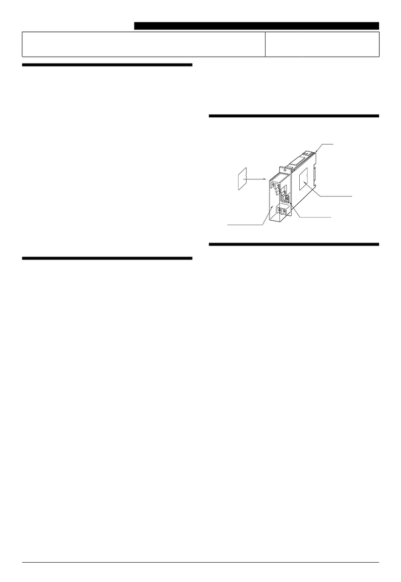
r~OTES
1.
MOUNT
ON
BOTTOM
OF PCB
2.
MOUNT
SO
BODY
OF CO[\'IPONENT
[S
i/8"
TO 3/'16"
ABOVE
PCB
3. 52 UH FERRITE CORE TORROIOp.L
SCG
#.
184·i005
L
QUANTITY
EQUALS
LENGTH
[h)
[NCHES
5.
USE A THIN
COAT
OF
THERMAL
HEATSfNK
COfViPOUND
6.
6X
CRYSTAL,
STANDARD
TOLERANCE,
10KHZ
SPAC[NG
POWER
SUPPLY
ASSEMBLY
PIN
6807-A
Symbol
Qty
Description
Part
#
1 1
POWER
SUPPLY
PCA
671-6018
R1
'1
RES. 1K OHM
1/2W,
5%
762-2121
R2 1 RES. 390 OHM
1/2W,
5%
762-2111
C:R2
1 DIODE,
ZENER
1N4751A-30 781-1081
CR3 1 RECTIFIER, 1
N4007-1000V
781-1037
DL
1 LED, T 1 % RED 473-1006
C2 1
CAP
220UF
AL
CAP
50V
-10/+50%
172-2132
C3 1
CAP
6800UF
AL
CAP
25V
-10/+50%
172-2228
F1
1 FUSE 2
Y2
AMP,
250V
SLOW
BLOW
691·1017
1
QUICK
FIT FUSE
COVER
699-1020
2 2 FUSE
CUPS,
PC
MOUNT
699-1001
From the library of WØMTU
This manual suits for next models
1
Table of contents
Other LPB Transmitter manuals
Popular Transmitter manuals by other brands

Lectrosonics
Lectrosonics MM400C instruction manual

Magnetek
Magnetek Telemotive MLTX manual

Avalon RF
Avalon RF OTX627 User's guide & operating manual

FlowLine
FlowLine EchoSonic LU05 owner's manual

Guangzhou Chuanzhou Electronic Technology
Guangzhou Chuanzhou Electronic Technology CZH-10A manual

Audio Resource Group
Audio Resource Group ARG-TX72ST user manual