Functional Schematic
Ordering Information1
1. Reference Application Note M513 for reel size information.
Pin Configuration
Part Number Package
MADR-011022-TR1000 1000 Piece Reel
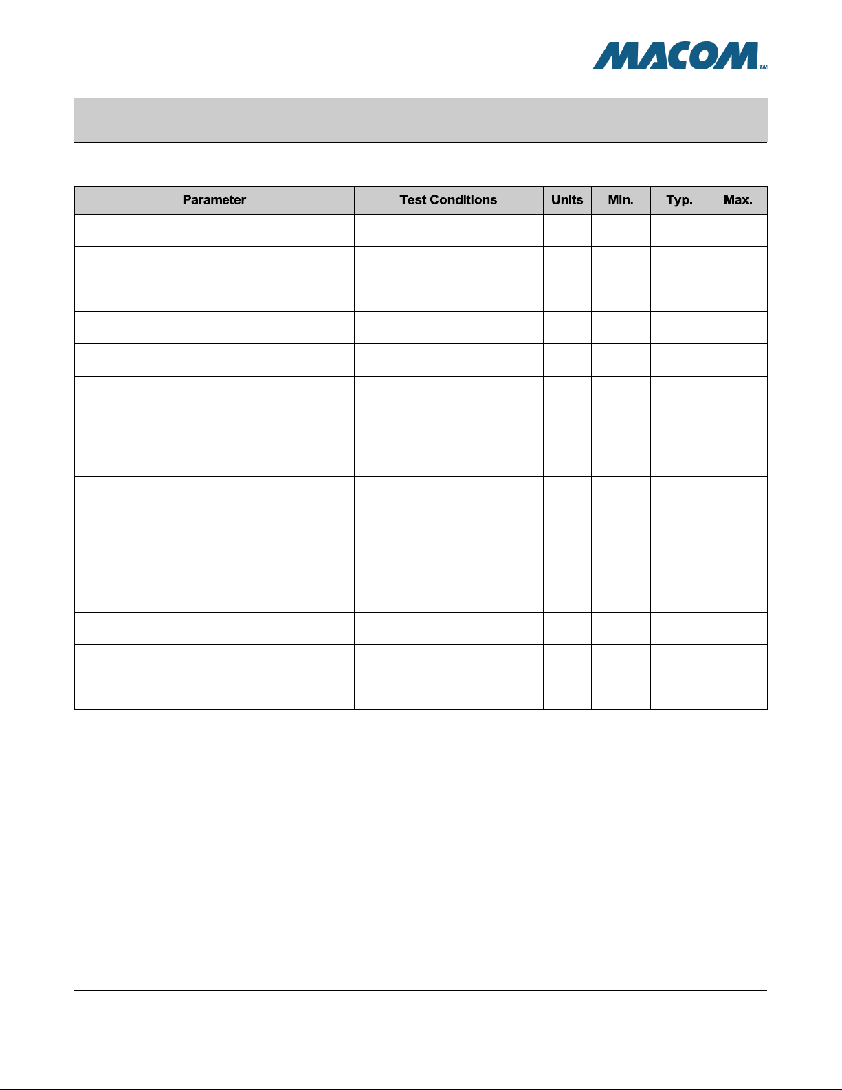
Pin # Function Description of Function
1C2 Logic Control Input
2C1 Logic Control Input
3GND Ground
4,5,7,8,9 NC2No Connection
6VEEB Negative Bias for Sequencer Die
10 VSEQ Power Sequencer Die Output
11 VEEA Negative Bias for Driver Die
12 VCC Positive Bias
13 DS Driver Select
14 BInverted Driver Output
15 ANon-inverted Driver Output
16 EN Enable
17 Paddle3Ground
2. NC pins should be left open.
3. MACOM recommends connecting the exposed pad centered
on the package bottom to RF, DC and thermal ground.
* Restrictions on Hazardous Substances, compliant to current RoHS EU directive.
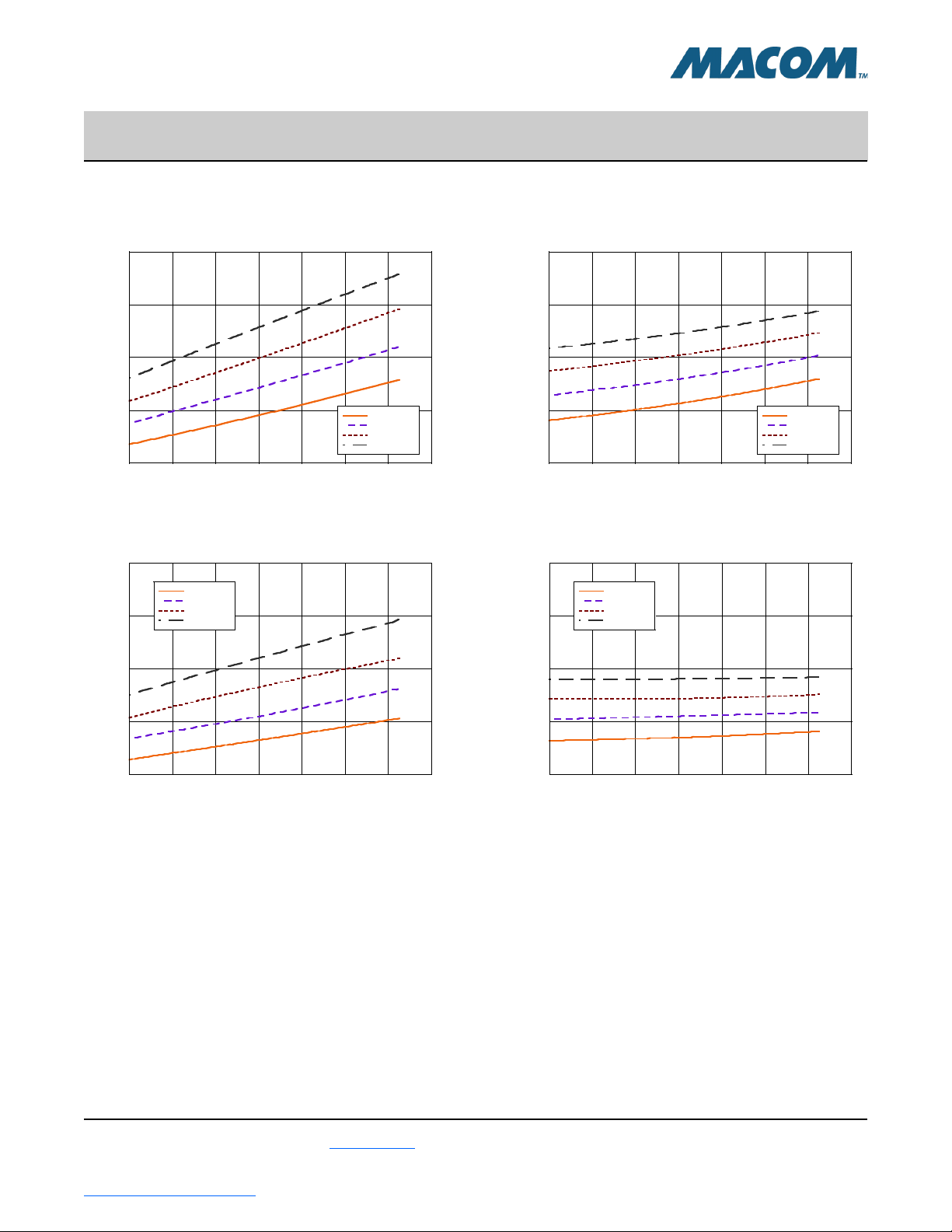
Features
• -10 V to -25 V Back Bias
• 25 mA Sinking Current
• 20 mA Sourcing Current
• Propagation Delay <130 ns Driving 100 pF
Capacitive Load
• Quiescent Currents <1 mA
• TTL Logic Control
• Internal Active Pull Down for All Logic Controls
• Internal Power Sequencer Eliminates External
Power Sequencing
• 4 mm 16-Lead PQFN Package
• RoHS* Compliant
Applications
• Aerospace & Defense
• ISM
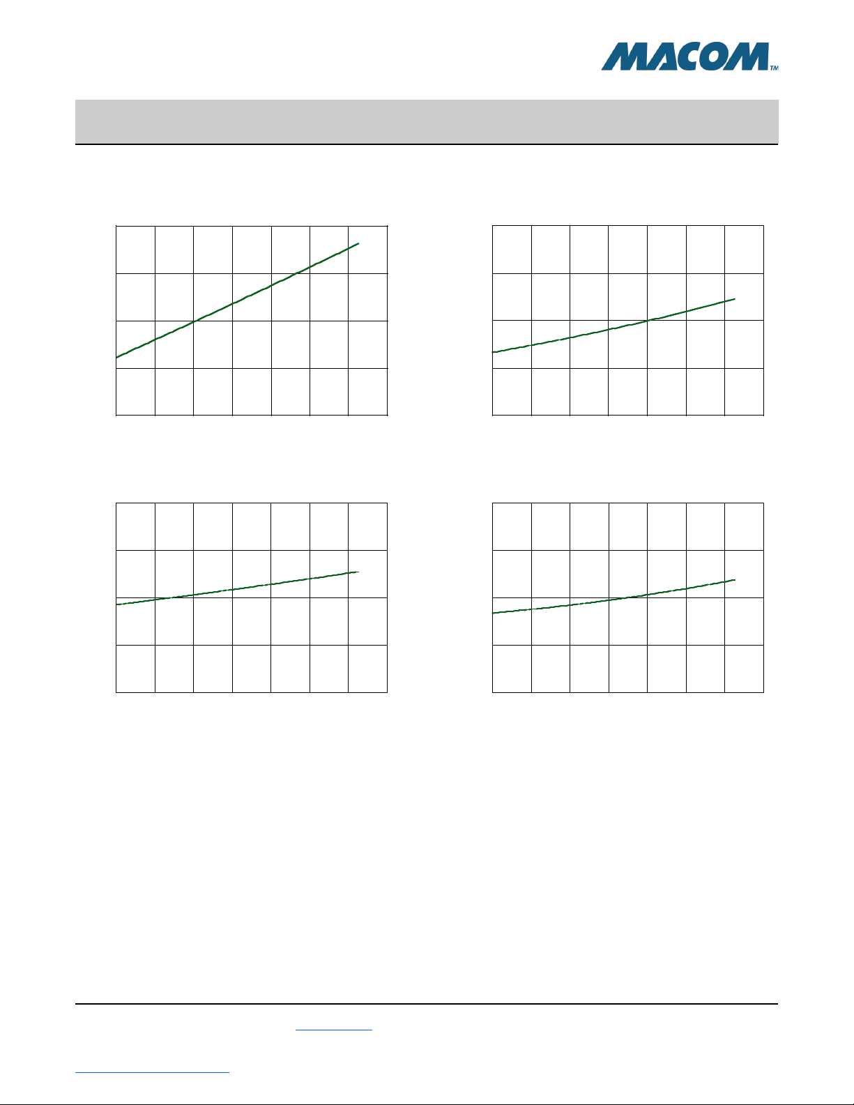
Description
The MADR-011022 switch driver is designed to work
with MACOM’s HMIC 20 W CW SPDT PIN diode
switches. This driver has complementary outputs
which can provide up to 25 mA sinking and 20 mA
sourcing bias current to a SPDT PIN diode switch.
An all-off RF state can be achieved with the EN pin
of this driver. An extra control C2 with driver select
DS are provided to allow two drivers working
together to drive a SP3T or SP4T switch.
The back bias voltage can be selected to be any
voltage between -10 V and -25 V. This switch driver
can be easily controlled by standard TTL logic. With
low quiescent current, this driver has a typical delay
of <130 ns when driving a 100 pF capacitive load.
This driver is packaged in a lead-free 4 mm 16-lead
PQFN package and is available in tape and reel
packaging for high volume applications.