TABLE
OF
CONTENTS
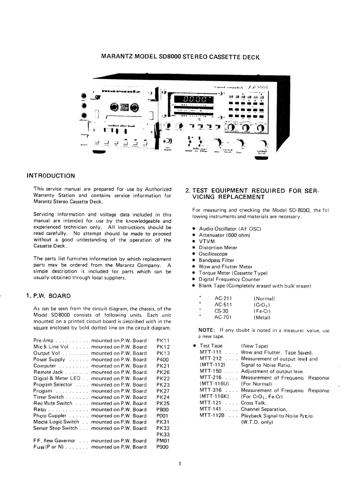
INTRODUCTION
isis
Mosse
wae
ba
Bet
ete
ak
Matos
Rem
re
len
oe
oe
oon
Wales
be
1
Te
DP
WEBOARD
26s
2
pice
Gith
acelde
et
ete
tilocet
Ae
2
hon
stare
seat
het
a
tt
ecca
ute
ae
Sela
Ae
A
teen
ees
oe
ts
x
Bead
Ma
1
2.
TEST
EQUIPMENT
REQUIRED
FOR
SERVICING
REPLACEMENT
.........................22...
1
3x
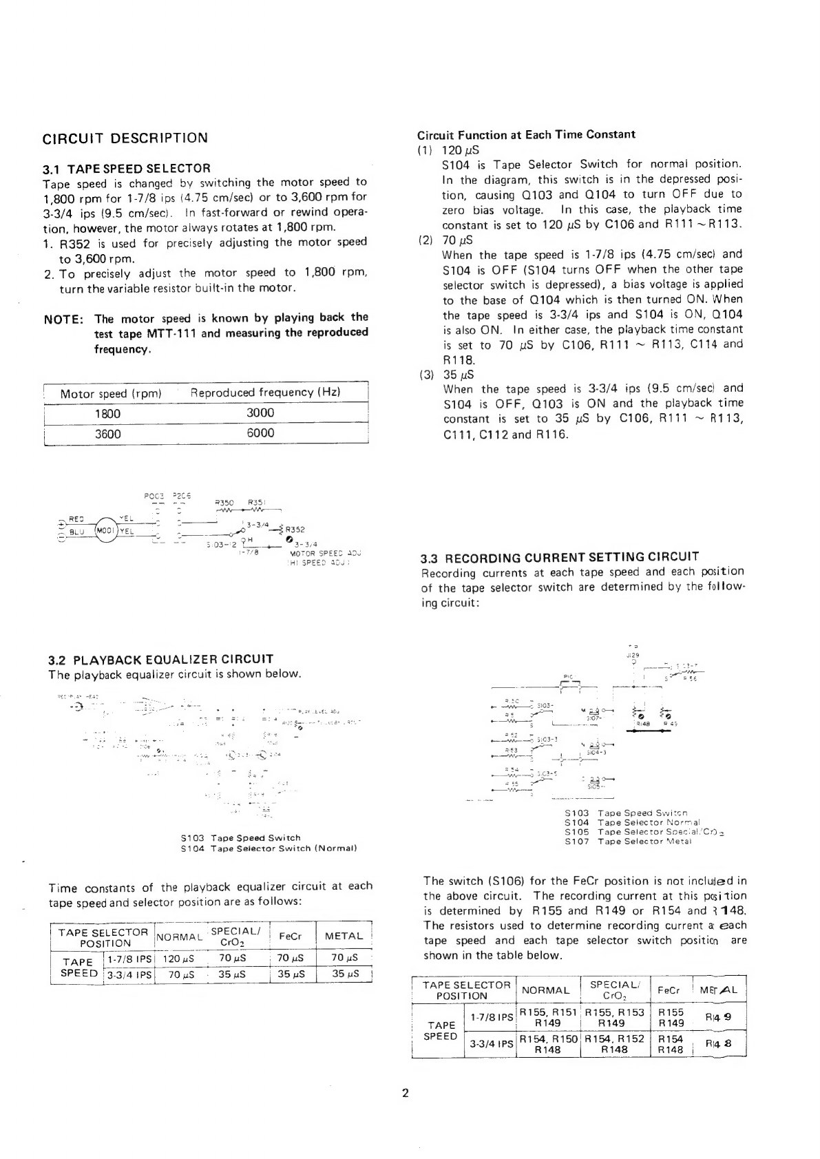
SCURCUIT-DESCRIPTION:
sco
coe
cst
Moe
a
eee
anes
ete
pail
eal
oi
bn
gee
oe
may
hee
ake
2
3.1-
“TAPE:SPEED
SELECTOR:
202%.
2's,
ois.
descete
hoe
ne
P24
Gicn
cee
hare
ae
ee
Rieke
aol
a
ed
OR
ee
ee
2
2
3.2
PLAYBACKEQUALIZER
CIRCUIT
.......0..
0.0.0...
cee
eee
ce
ett
eevee
eben
eeny
2
3.3.
RECORDING
CURRENTSETTING
CIRCUIT
........
0...
0...
ccc
ee
cece
ee
een bee
neces
2
3.4
RECORDING
COMPENSATING
CIRCUIT
........
0.00...
cc
eee
beeen
bbnens
3
3.5
BIAS
OSCILLATOR
CIRCUIT/ERASE
OSCILLATOR
CIRCUIT
...........
0.0...
e
eee
eenee
3
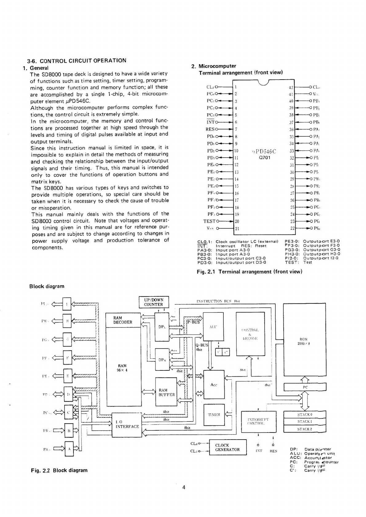
3.6
CONTROL
CIRCUIT
OPERATION
.........
2.0...
0...
cece
ce
te
ee
eee
eee
b
eee
enes
4
&.
(DISASSEMBLE
©
2.02532
sce
4
sevraiseels
wont
aie
fal
oahu
ins
ould
Seette
clues
hued
Sad
doe
e
ae
tele
29
5.
MECHANICAL
ADJUSTMENT
......000
0.0.00
ccc
eee
ence
bebe
been
beenenes
31
§:°
-ELEGTRICAL:ADIJUSTIMENT.
24.6.3
6)neca
seb
eee
¥
ee
ide
ep
en
Rll
chord
wha
eek
wade
obo
wee
33
7,
VOLTAGE
CONVERSION
FOREUROPEANMODEL
............
0.0...
cc
cece
cece
ceeeneee
43
8.
DIAGRAM
AND
COMPONENT
LOCATIONS
..........
0.0...
ccc
ccc
cece
cece
ececeeee
44
8.1.
Pre
Amp.
Assembly
(PK11)
Schematic
Diagram
and
Component
Locations
............
0000
ce ce
eeceecccue
44
8.2
Mic
Line
Volume
Assembly
(PK12)
Schematic
Diagram
and
Component
Locations..............-.c0ccceccee
44
8.3
Output
Volume
Assembly
(PK13)
Schematic
Diagram
and
Component
Locations
.............-..cccceecee
44
8.4
Computer
Assembly
(PK21)
Schematic
Diagram
and
Component
Locations
............0
000 ccc
eececceccee
47
8.5
Program
Selector
Assembly
(PK23)
Schematic
Diagram
and
Component
Locations..............0cc0ceeeeeee
49
8.6
Power
Supply
and
Bias
OSC
Assembly
(P400)
Schematic
Diagram
and
Component
Locations.................-..
50
8.7
Digital
and
Meter
LED
Assembly
(PK22)
Schematic
Diagram
and
Component
Locations
...............e0ce0ee
50
8.8
Timer
Switch
Assembly
(PK24)
Schematic
Diagram
and
Component
Locations.
.............
ccc
ce cee
eeccue
51
8.9
Rec-Mute
Switch
Assembly
(PK25)
Schematic
Diagram
and
Component
Locations.
..............-0cecccccee
51
8.10
Program
Select
Assembly
(PK27)
Schematic
Diagram
and
Component
Locations
.............0.
0c
cee
eeeceee
52
8.11
Logic
Control
Assembly
(PK31)
Schematic
Diagram
and
Component
Locations...
...........0cce
cee
eeeeee
52
8.12
Remote
Jack
Assembly
(PK25)
Schematic
Diagram
and
Component
Locations
............00.
ccc
cee
cceucee
52
8.13
Safety
Switch
Assembly
(PK32)
Schematic
Diagram
and
Component
Locations.
............0.0
cece
ceeecevae
52
8.14
Safety
Switch
Assembly
(PK33)
Schematic
Diagram
and
Component
Locations...............-00cecceccecae
52
8.15
Timer
Relay
Assembly
(P800)
Schematic
Diagram
and
Component
Locations.............00
ccc
cee
eeceunes
53
8.16
Fuse
Assembly
(P900)
Schematic
Diagram
and
Component
Locations
(N,
TASB
VERSIONS
ONLY)
25:3.
2c8i
2
ehowal
ia
be
deursea
& 4
tur
ach
ead
wow
aa
eM
ee
Tae
ot
eee
53
8.17
Motor
Governor
Assembly
(PMO1)
Schematic
Diagram
and
Component
Locations
..............-0.e0ccceeee
54
8.18
Photo
Coupler
Assembly
(P001)
Component
Locations...
2...
ce
eee
eben
b
ebb
ens
54
Hi.
BOC
RD
EAG
HAM
75s
cece
anon
4.ai
apne
sah,
chk
seoelave
sow
den
sauclie
ay
woes
a
A
BS
ty
ec
tee
Re
55
10.
EXPLODED
VIEWANDPARTS
LIST
2.00.00.
occ
cece
cece
cece
bbe
eee
bebe
ee
eee.
56
Wy
CELEGTRICAL
PARTS
UIST:
2
coh
wOahven
oe
ice
ban
eae
ee
ee
as
Bie
enn
aed
wd
oe
Pande
dig
Lee
57
t2)
“TE
CHNIGAL
SPECIFICATIONS:
«cu:
i-aosscyd
x
ack
dee
St
a4
Gok
eo
ead
ache
hb
gehediow's
bkarke
ele
dhs
77
13.
SCHEMATIC
DIAGRAM
.......
0.0.
cect
ebb
b
been
bbe
beceeeneeay
78