Sanyo MCD-ZX700F User manual

Service Manual
FILE NO.
REFERENCE No. SM5810290
CD Portable Radio
Cassette Recorder
MCD-ZX700F
(XE)
PRODUCT CODE No.
164 081 00
CONTENTS
Specification ..................................................................... 1
Laser beam safety precaution .......................................... 1
Tuner Adjustment ............................................................. 2
Tape Deck Adjustment ..................................................... 3
IC Block Diagram & Description ....................................... 3,7
Exploded View (Cabinet & Chassis) ................................ 4
Parts List .......................................................................... 5
Exploded View & Parts List(Tape Deck) ......................... 7
Wiring Connection ............................................................ 11
Schematic Diagram (Micom) ............................................ 12
Schematic Diagram (CD) ................................................. 14
Schematic Diagram (Radio) ............................................. 16
Schematic Diagram (Audio) ............................................. 18
Wiring Diagram (CD Main/Amp/Tu) ............................... 20
Wiring Diagram (Rectifier, Display, Power) .................... 21

- 1 -
CD CHANGER SECTION
Channels ..................................... 2-channel stereo
Sampling frequency .................... 44.1 kHz
Pick-up ........................................ semiconductor laser
Laser output ................................ 0.6 mW (Continuous wave max.)
Wave length ................................ 790 nm
Wow and Flutter .......................... Below measurable limits
Radio
Reception frequency
FM ........................................... 87.5 - 108 MHz (500 kHz step)
AM ...........................................522 - 1,710 kHz (9 kHz step)
CASSETTE DECK
Track system ............................... 4 - track, 2 - channel stereo
Erasing system ........................... Magnet erase
Tape speed ................................. 4.75 cm/sec
Frequency response ................... 80 - 12,000 Hz
Fast forward and Rewind time .... Approx. 110 sec. (C - 60)
SPECIFICATIONS
• Pickup that emits a laser beam is used on this CD section.
CAUTION :
USE OF CONTROLS OR ADJUSTMENTS OR
PERFORMANCE OF PROCEDURES OTHER
THAN THOSE SPECIFIED HEREIN MAY RESULT
IN HAZARDOUS RADIATION EXPOSURE.
LASER OUTPUT................ 0.6 mW Max. (CW)
WAVE LENGTH ................. 790 nm
LASER BEAM SAFETY PRECAUTION
GENERAL SECTION
Output power .............................. 3 W/ch (DC max.)
Speaker ....................................... 10 cm X 2
Terminal ...................................... PHONE : 32
Power source .............................. AC : 110 - 120/220 - 240 V , 50/60 Hz
.................................................... DC : 12V, 8 "R20/D" batteries
Dimensions ................................. Approx. 480(W) x 167(H) x 258(D)
mm
Weight (approx.) ......................... 3.0 kg (without batteries)
Specifications subject to change without notice.
CAUTION – INVISIBLE LASER RADIATION WHEN OPEN AND
INTERLOCKS DEFEATED. AVOID EXPOSURE TO BEAM.
ADVARSEL – USYNLIG LASER STRÅLING VED ÅBNING, NÅR
SIKKERHEDSAFBRYDERE ER UDE AF FUNKTION, UNDGÅ UDS ÆTTELSE
FOR STRÅLING.
VARNING – OSYNLIG LASER STRÅLNING NÄR DENNA DEL ÄR ÖPPNAD
OCH SPÄRR ÄR URKOPPLAD. STRÅLEN ÄR FARLIG.
VORSICHT – UNSICHTBARE LASERSTRAHLUNG TRITT AUS, WENN
DECKEL GEÖFFNET UND WENN SICHERHEITSVERRIEGELUNG
ÜBERBRÜCKT IST. NICHT, DEM STRAHL AUSSETZEN.
VARO – AVATTAESSA JA SUOJALUKITUS OHITETTAESSA OLET ALTTIINA
NÄKYMÄTTÖMÄLLE LASERSÄTEILYLLE. ÄLÄ KATSO SÄTEESEEN.

- 2 -
TP4
TP3
TP7
CT102
T101
L102
TP1
L101
TP2
TP6 CT101 TP5 TP8 TP9
• Use a plastic screw driver for adjustments.
• Adjust the intermediate frequency of AM and FM to the frequency of ceramic filter.
• Set of unit
Supply voltage : DC 12V
Speaker : 32
Function switch : RADIO
PARTS LOCATION
TUNER ADJUSTMENTS
This is a basic adjustment.
1. AM ADJUSTMENT
Step Adjusting Tuning Adjust- VTVM
Circuit Frequency Instrument Input Instrument Output ment Oscilloscope
1IF 999 KHz AM sweep Loop ANT. VTVM Speaker T103 Max.
(450 KHz) generator oscilloscope
2Tuning 522 KHz --- --- Digital TP7(H) T101 1.5V±0.05V
3coverage 1611 KHz --- --- voltmeter TP2(E) --- 7.4V±0.1V
4Tracking 603 KHz AM signal Loop ANT. VTVM Speaker AM COIL Max.
51404 KHz generator oscilloscope CT102
Input Connection Output Connection
1. FM ADJUSTMENT BAND SELECT SWITCH : FM FM Dummy Antenna:75Ωunbalance
Step Adjusting Tuning Adjust- VTVM
Circuit Frequency Instrument Input Instrument Output ment Oscilloscope
1IF98.0MHz FM sweep TP3(H) VTVM TP5(H) --- Non Adjustmen
t
10.7NHz generator TP4(E) oscilloscope TP4(E)
2Tuning 87.5Hz --- --- Digital TP6(H) L102 2.0V±0.1V
3coverage 108.0MHz --- --- voltmeter TP2(E) --- 7.2V±0.1V
4Tracking 90.0.MHz FM signal TP1(H) VTVM TP8(H) L101 Max.
5106.0MHz generator TP2(E) oscilloscope TP9(E) CT103
Input Connection Output Connection

- 3 -
2. HEAD AZIMUTH ADJUSTMENT
(1) Load the test tape(VTT-703, etc., 10 kHz) for azimuth
adjustment.
(2) Press the PLAY button.
(3) Use a cross-tip screwdriver to turn the screw for azimuth
adjustment so that the left and right output are maximized.
(4) Press the STOP button.
(5) After completion of the adjustment, use thread lock(TB-1401B)
to secure the azimuth-adjustment screw.
4. MOTOR SPEED ADJUSTMENT
(1) Insert the test tape(TCC-119, etc., 3,000 Hz).
(2) Press the PLAY button.
(3) Use a flat-tip screwdriver to turn the SVR(located inside the
rear of the motor) to adjust SVR so that the frequency counter
become 3,000 Hz.
5. CHECKING THE MECHANISM TORQUES AND TENSION
• Clean the head, capstan and pinch roller before making any measurement.
Measurement Take-up torque Back tension Tape tension
Cassette for PLAY : TW-211A PLAY : TW-2111A Drive-power cassete
measurement F.FW/REW : TW-2231 TW-2412
PLAY 30 - 60 gr.cm 2.0 - 4.5 gr.cm 60 gr or more.
F.FWD 55 - 120 gr.cm. ----- -----
REW 55 - 120 gr.cm. ----- -----
1. HEAD REPLACEMENT
• After replacement, demagnetize the heads by using a degausser.
• Be sure to clean the heads before attempting to make any adjustments.
• All wiring should be returned to the original position after work is completed.
TAPE DECK ADJUSTMENTS
This is a basic adjustment.
3. AC BIAS FREQUENCY ADJUSTMENT
(1) Connect counter to T201(BS).
(2) R/P switch in recording state.
(3) Adjustment T801 a plastic screw , AC bias frequency : 80 kHz.
IC903 LA6541D(CD Driver)
123456 789
10 11 12
131415161718192021222324
Vcc Vref VIN4 VG4 Vo8 Vo7 GND Vo6 Vo5 VG3 VIN3 CD RES
Vcc Mute VIN1 VG1 Vo1 Vo2 GND Vo3 Vo4 VG2 VIN2 Reg OUT Reg IN
Vcc
11k 11k
11k11k
Level
Sift BTL
Driver BTL
Driver Level
Sift RESET
Regulator
Level
Sift
BTL
Driver
Level
Sift BTL
Driver
IC BLOCK DIAGRAM & DESCRIPTION

- 4 -
EXPLODED VIEW(CABINET & CHASSIS)
12
3
7
8
Y01
Y01
Y02
Y04
Y05
Y09
Y09
Y14
Y16
Y17
Y15
Y18
Y18
Y18
60
Y20
Y20
Y18 Y21
Y18
Y18
Y10
Y11
Y11
Y12
Y13
Y13
Y12
Y03
Y03
8
9
51
51
52
53
71 72
15
14
1718 19
21
23
27
28
29
31
74
56
73
32
33 58
59
57
34 38
32
30
54
55
26
16
11
4
39
40
Y06

- 5 -
PARTS LIST
CAUTION : Regular type resistors and capacitors are not listed. To know those values, refer to the schematic diagram.
Regular type resistors are less than 1/4W carbon type and 0 ohm chip resistors.
Regular type capacitors are less than 50V and less than 1000µF of Ceramic type and Electrolytic type.
PRODUCT SAFETY NOTICE
EACH PRECAUTION IN THIS MANUAL SHOULD BE FOLLOWED DURING SERVICING. COMPONENTS IDENTIFIED WITH
THE IEC SYMBOL !
!! IN THE PARTS LIST AND THE SCHEMATIC DIAGRAM DESIGNATE COMPONENTS IN WHICH SAFETY
CAN OF SPECIAL SIGNIFICANCE. WHEN REPLACING A COMPONENT IDENTIFIED , USE ONLY THE REPLACEMENT
PARTS DESIGNATED, OR PARTS WITH THE SAME RATINGS OF RESISTANCE, WATTAGE OR VOLTAGE THAT ARE
DESIGNATED IN THE PARTS LIST IN THIS MANUAL. LEAKAGE-CURRENT OR RESISTANCE MEASUREMENTS MUST
BE MADE TO DETERMINE THAT EXPOSED PARTS ARE ACCEPTABLY INSULATED FROM THE SUPPLY CIRCUIT
BEFORE RETURNING THE PRODUCT TO THE CUSTOMER.
REF.NO. PART NO. DESCRIPTION
PACKING & ACCESSORIES
REF.NO. PART NO. DESCRIPTION
645 055 7705 INSTRUCTION MANUAL
645 027 2073 POLY BAG,PWR CORD
645 044 1943 POLY BAG,I/B
645 035 1334 POLY BAG PE 18 X 24,UNIT
645 055 7804 POLY FOAM,2 PCS LEFT&RIGHT
645 055 7927 CARTON CASE
645 023 3463 POWER CORD,VDE APP
645 055 6760 REMOTE CTL,RC24-102000-070
CABINET & CHASSIS
REF.NO. PART NO. DESCRIPTION
1645 055 7620 CASS DOOR LENS
2645 055 6746 ASSY CASS LID
3645 055 7798 CASS DOOR SPRING
4645 055 7484 KNOB ROTARY,VOL
7645 055 6708 ASSY CABINET
8645 033 0360 SPK CLIP
9645 055 7613 KNOB POWER CTL
11 645 033 4252 ASSY,GEAR CASS DOOR
14 645 055 7354 KNOB CASS PAUSE
15 645 055 7361 KNOB CASS STOP/EJECT
16 645 055 7378 KNOB CASS FFWD
17 645 055 7385 KNOB CASS REWIND
18 645 055 7392 KNOB CASS PLAY
19 645 055 7408 KNOB CASS RECORD
21 645 055 7347 HANDLE
23 645 055 6739 ASSY CD LID
26 645 042 0351 CD DOOR SPRING
27 645 055 7552 CD TRAY,TOP PANEL
28 645 055 7576 KNOB CD DOOR,OPEN
29 645 055 7545 CD DOOR LOCK
30 645 042 9378 ASSY GEAR CD DOOR
31 645 042 0375 CD MECHA COVER
32 645 033 3446 RUBBER SILICON
33 645 033 0391 AC SKT COVER
34 645 055 6692 ASSY CABINET REAR
38 645 055 7477 BATTERY LID
39 645 055 7651 FRONT CAB LENS
40 645 054 0776 CD DECK MECHANISM,13933162
FIXING PARTS
REF.NO. PART NO. DESCRIPTION
Y01 645 027 1168 SCR 3X8,SPK
Y02 645 023 6624 SCREW ST 3X10,POWER KNOB
Y03 645 023 6617 SCREW ST 3X10,CD CTL BD
Y04 645 027 1168 SCR 3X8,CASS DOOR GEAR
Y05 645 023 6617 SCREW ST 3X10,CASS DECK
Y06 645 027 1168 SCR 3X8,CD DOOR GEAR
Y10 645 033 4276 SCR 2X6,CD MICRO SW
Y11 645 027 1373 WASHER METAL
Y12 645 033 0247 SCR 2.6X8,CD DECK
Y13 645 023 6594 SCREW ST 3X8,MAIN BD
Y14 645 027 1182 SCR 3X20,X’FORMER
Y15 645 027 1328 SOLDERING SLUG
Y16 645 027 1144 SCR 2.8X12,AC SOCKET
Y17 645 023 6594 SCREW ST 3X8,RECTIFIER BD
Y18 645 027 1199 SCR 3X30,F CAB TO R CAB
Y20 645 023 6648 SCREW ST 3X12,
CD TRAY TO F CAB
Y21 645 027 1236 SCR 3X8,RADIO ANT
ELECTRICAL-PARTS
REF.NO. PART NO. DESCRIPTION
51 645 055 6777 SPK 4, SPK
52 645 055 7231 13P FFC CABLE,TO CTL BD CN702
53 645 055 7248 15P FFC CABLE,TO CTL BD CN701
54 645 043 9780 LEAF SW,CD LID SW
55 645 055 7255 16P FFC CABLE,TO CD DECK
56 645 042 0184 HSG 1PIN,FM ANT
57 645 041 9881 PWR TRANS,V3023FS
58 645 032 9760 AC SOCKET S-1-1225,VDE
59 645 055 7149 FUSE GLASS TUBE,FS1101
60 645 041 9928 ROD ANTENNA,2 SECTION
POWER P.W.BOARD ASSY
REF.NO. PART NO. DESCRIPTION
71 614 324 1850 ASSY,PWB POWER(Only initial)
SW711 645 042 0023 SW TACT,POWER ON /OFF
DISPLAY P.W.BOARD ASSY
REF.NO. PART NO. DESCRIPTION
72 614 324 1843 ASSY,PWB DISPLAY(Only initial)
C0709 645 055 6784 GOLD CAP DX-5R5H104
CN701 645 033 3675 FFC HEADER 15PINS
CN702 645 034 8440 FFC HEADER 13PINS
D0701 645 055 6821 DIODE 1N4148
D0703 645 055 6821 DIODE 1N4148
D0708 645 055 6821 DIODE 1N4148
D0709 645 055 6821 DIODE 1N4148
D0710 645 055 6821 DIODE 1N4148
D0711 645 055 6821 DIODE 1N4148
D0713 645 055 6821 DIODE 1N4148
D0715 645 055 6821 DIODE 1N4148
D0716 645 055 6821 DIODE 1N4148
D0717 645 055 6821 DIODE 1N4148
D0720 645 055 6821 DIODE 1N4148
D0721 645 055 6821 DIODE 1N4148
D0722 645 055 6821 DIODE 1N4148
D0726 645 055 6821 DIODE 1N4148
D0727 645 055 6821 DIODE 1N4148
D0729 645 055 6821 DIODE 1N4148
ED701 645 054 0615 LED ROUND TYPE,LED701
IC701 645 055 7040 IC LC587008 1P08
IC702 645 055 6951 IC PST600C
IC703 645 055 6968 IC PST600L
IR701 645 033 3477 DIODE RPM-6938-V4
L0701 645 034 6729 INDUCTOR 100UH
L0702 645 034 6729 INDUCTOR 100UH
LD701 645 055 7071 LCD DISPLAY,LCD701
Q0702 645 055 6890 TR 2SC3400AC
Q0703 645 055 6852 TR DTA114TS
Q0705 645 055 6890 TR 2SC3400AC
Q0706 645 055 6890 TR 2SC3400AC
Q0708 645 055 6890 TR 2SC3400AC
Q0709 645 032 9890 TR KTC-9015C
Q0710 645 055 6890 TR 2SC3400AC

- 6 -
PARTS LIST
REF.NO. PART NO. DESCRIPTION
Q0711 645 032 9890 TR KTC-9015C
Q0712 645 055 6890 TR 2SC3400AC
SW701 645 042 0023 SW TACT,TAPE
SW702 645 042 0023 SW TACT,TUN / BAND
SW703 645 042 0023 SW TACT,FM MODE/RANDOM
SW704 645 042 0023 SW TACT,PERSET/REPEAT
SW705 645 042 0023 SW TACT,MEMORY
SW706 645 042 0023 SW TACT,BASS
SW707 645 042 0023 SW TACT,STOP
SW708 645 042 0023 SW TACT,B-SKIP
SW709 645 042 0023 SW TACT,CD /PLAY
SW710 645 042 0023 SW TACT,F-SKIP
VR701 645 055 7309 ROTARY ENCODER
X0701 645 055 7101 RESONATOR 4MHZ
X0702 645 055 7125 CRYSTAL
645 055 7521 DISPLAY BKT
645 055 7538 LED BKT
CD MAIN/AMP/TU P.W.BOARD ASSY
REF.NO. PART NO. DESCRIPTION
73 614 324 1836 ASSY,PWB CD MAIN/AMP/TU
(Only initial)
C0108 645 055 6791 POLY CAP 390PF
C0123 403 057 7501 POLYESTER 0.012U K 50V
C0124 403 057 7501 POLYESTER 0.012U K 50V
C0206 403 056 7908 POLYESTER 1000P K 50V
C0207 403 056 7908 POLYESTER 1000P K 50V
C0212 403 060 8205 POLYESTER 0.033U K 50V
C0213 403 060 8205 POLYESTER 0.033U K 50V
C0218 403 056 7908 POLYESTER 1000P K 50V
C0219 403 056 7908 POLYESTER 1000P K 50V
C0311 403 057 2803 POLYESTER 0.1U K 50V
C0312 403 057 2803 POLYESTER 0.1U K 50V
C0513 403 060 0506 POLYESTER 2700P K 50V
C0514 403 060 0506 POLYESTER 2700P K 50V
C0801 403 059 5901 POLYESTER 0.022U K 50V
C0802 403 057 0403 POLYESTER 0.01U K 50V
C0804 403 059 3600 POLYESTER 2200P K 50V
C0901 403 057 2803 POLYESTER 0.1U K 50V
C0902 403 060 8205 POLYESTER 0.033U K 50V
C0905 403 060 6102 POLYESTER 3300P K 50V
C0906 403 062 0306 POLYESTER 0.047U K 50V
C0907 403 058 5209 POLYESTER 0.15U K 50V
C0910 403 056 7908 POLYESTER 1000P K 50V
C0911 403 057 2803 POLYESTER 0.1U K 50V
C0912 403 058 3205 POLYESTER 0.015U K 50V
C0913 403 058 9900 POLYESTER 0.018U K 50V
C0920 403 059 3600 POLYESTER 2200P K 50V
C0923 403 060 8205 POLYESTER 0.033U K 50V
C0944 403 057 2803 POLYESTER 0.1U K 50V
C0970 403 058 5209 POLYESTER 0.15U K 50V
CF101 645 055 6937 BAND PASS FILTER
CF102 645 055 6913 CERAMIC FILTER
CF103 645 055 6913 CERAMIC FILTER
CF104 645 055 6906 CERAMIC FILTER
CF105 645 055 6920 CERAMIC FILTER
CN101 645 042 0177 FFC HEADER 15PINS
CN201 645 055 7170 5P HEADER
CN301 645 027 3803 WAFER 4P
CN401 645 027 3803 WAFER 4P
CN403 645 032 9982 HEADER 3PINS
CN901 645 055 7163 16P FFC HEADER
CN903 645 034 6781 FFC HEADER 13PINS
CN904 645 034 6798 HEADER 2PINS
CT101 645 023 6310 TRIMMER 10PF
CT102 645 023 6310 TRIMMER 10PF
D0101 645 055 6821 DIODE 1N4148
D0102 645 055 6821 DIODE 1N4148
D0103 645 055 6821 DIODE 1N4148
D0104 645 055 6821 DIODE 1N4148
D0105 645 055 6821 DIODE 1N4148
D0106 645 055 6821 DIODE 1N4148
D0301 645 055 6821 DIODE 1N4148
D0302 645 055 6821 DIODE 1N4148
D0303 645 023 6112 RECTIFIER 1N-4001
D0304 645 055 6821 DIODE 1N4148
D0305 645 055 6821 DIODE 1N4148
D0306 645 055 6821 DIODE 1N4148
D0307 645 055 6821 DIODE 1N4148
D0308 645 055 6821 DIODE 1N4148
D0309 645 055 6821 DIODE 1N4148
D0310 645 055 6821 DIODE 1N4148
D0311 645 055 6821 DIODE 1N4148
D0312 645 055 6821 DIODE 1N4148
D0313 645 055 6821 DIODE 1N4148
D0402 645 055 6821 DIODE 1N4148
D0901 645 055 6821 DIODE 1N4148
D0902 645 055 6821 DIODE 1N4148
IC101 645 055 6975 IC LA1823ESIA
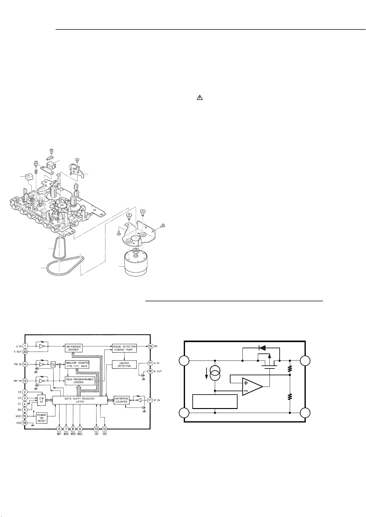
IC102 645 055 7019 IC LC72131
IC201 645 055 6999 IC TA8142AP
IC301 645 032 9920 IC LA-4227
IC401 645 055 6982 IC KIA7808P
IC402 645 055 7033 IC S81256SGYX
IC501 645 055 7026 IC LC75342
IC901 645 055 7002 IC LA9241M
IC902 645 033 4740 IC LC78622E
IC903 645 033 4702 IC LA6541D
JK301 645 033 3743 EARPHONE JACK
L0101 645 049 9913 FM COIL 4.5T
L0102 645 027 0345 VHF COIL
L0105 645 027 0352 CHOKE COIL 100UH
L0301 645 044 1721 FERRITE BEAD
L0302 645 044 1721 FERRITE BEAD
L0303 645 044 1721 FERRITE BEAD
L0501 645 034 7177 INDUCTOR 1000UH
L0901 645 042 0108 CHOKE COIL 26UH
Q0107 645 034 6866 TR 2SC2839E
Q0108 645 034 7078 TR 2SC3330U
Q0109 645 027 0420 TR 8050C
Q0110 645 055 6876 TR 9018F
Q0301 645 033 3538 TR 2SD1936S AC
Q0302 645 033 3538 TR 2SD1936S AC
Q0303 645 023 6129 TR 9014C
Q0304 645 023 6129 TR 9014C
Q0305 645 023 6129 TR 9014C
Q0401 645 055 6883 TR KSA928A
Q0402 645 023 6129 TR 9014C
Q0403 645 055 6869 TR 8550B C
Q0404 645 023 6129 TR 9014C
Q0405 645 027 0420 TR 8050C
Q0407 645 055 6869 TR 8550B C
Q0408 645 023 6129 TR 9014C
Q0409 645 027 0420 TR 8050C
Q0801 645 027 0420 TR 8050C
Q0803 645 023 6129 TR 9014C
Q0901 645 033 3538 TR 2SD1936S AC
Q0902 645 033 3538 TR 2SD1936S AC
Q0903 645 033 3538 TR 2SD1936S AC
Q0904 645 033 3538 TR 2SD1936S AC
Q0905 645 033 3521 TR 2SA1317S AC
Q0907 645 033 3514 TR 2SB764D
Q0908 645 041 9959 TR 2SA1346AC
Q0909 645 033 3538 TR 2SD1936S AC
Q0910 645 033 3538 TR 2SD1936S AC
R0329 402 071 1304 FUSIBLE RES 2.2 JA 1/4W
SW100 645 055 7064 SW TACT,RESET
SW201 645 023 6327 SW RECORDING PS62D01-S,SH
T0101 645 055 6944 IFT,OSC 1A612R
T0103 645 033 3866 AM COIL,IF 2070
T0801 645 027 0307 BIAS COIL,IFT 3630
VD101 645 055 6807 DIODE SVC201
VD102 645 055 6807 DIODE SVC201
VD103 645 055 6814 DIODE SVC348
X0101 645 055 7118 CRYSTAL
X0901 645 052 4837 RESONATOR 16.934MHZ
ZD101 645 055 6838 ZENER 5.6V
ZD401 645 055 6845 ZENER 13V

- 7 -
PARTS LIST
REF.NO. PART NO. DESCRIPTION
TM06
TM05
TM04
TM02
TM01
TM03
EXPLODED VIEW & PARTS LIST(TAPE DECK)
TAPE DECK MECHANISM PARTS LIST
REF.NO. PART NO. DESCRIPTION
645 050 1814 CASS DECK MECHANISM
TM01 645 018 0637 R/P HEAD
TM02 645 050 1401 PINCH ROLLER
TM03 645 030 6839 E HEAD
TM04 645 050 1395 RF BELT
TM05 645 050 1784 MAIN BELT
TM06 645 050 2101 ASSY,MOTOR
IC101 LC72131(PLL) IC402 S-81256G(Voltage Regulator)
23
1
REFERENCE
VOLTAGE
VIN VOUT
GND
IC BLOCK DIAGRAM & DESCRIPTION
RECTIFIER P.W.BOARD ASSY
REF.NO. PART NO. DESCRIPTION
74 614 324 1867 ASSY,PWB RECTIFIER(Only initial)
D1101 645 023 6112 RECTIFIER 1N-4001
D1102 645 023 6112 RECTIFIER 1N-4001
D1103 645 023 6112 RECTIFIER 1N-4001
D1104 645 023 6112 RECTIFIER 1N-4001
D1105 645 055 6821 DIODE 1N4148
F1101 645 055 7149 FUSE GLASS TUBE,FS1101
645 035 0511 FUSE HOLDER MW1010K
645 042 0320 HEAT SINK
645 027 1397 NUT,HEAT SINK
645 051 6474 FERRITE BEAD,
PRI OF X’FORMER TO AC SK
645 055 7095 FERRITE BEAD,CN401 TO CN1101
645 055 7200 HSG 4P,CN401 TO CN1101
645 042 0184 HSG 1PIN,FM ANT
645 042 0337 HEAT SINK
645 055 6685 ASSY BAR ANT

- 8 -
IC BLOCK DIAGRAM & DESCRIPTION
IC902 LC78622E(Degital Signal Processor)
EFMO VV
DD
VV
SS
PDO ISET FR PCK TAI
TST11
TEST1 TEST3 TEST5
TEST2 TEST4
V
DD
V
SS
C2F
DOUT
(NC)
LV
DD
LV
SS
MUTELLCHO
MUTER
RV
DD
RV
SS
RCHO
XV
DD
XOUT
XINFSX
XV
SS
4.2M16MEFLGEMPHCONT5
CONT4
CONT3
CONT2
CONT1
TGL
RESJP+JP-TOFFTESHFL
RWC
COIN
CQCK
SQOUT
WRQ
CS
SFSY
SBSY
SBCK
PW
V/P
CLV-
CLV+
FSEQ
EFMIN
DEFI
10
22
1
12
13
14
49
51
47
50
63
53
55
57
56
54
15 16 17 20 19 58 18 24 25 26 27 28 29 48 60 61 46 52 45 44 43 39 41 42 40 37 35 38 36
34
31
30
9
21
64357 2
59 64 11 32 33 62
8
23
Slice level
Control
Subcode Dxract
QCRC
Syncrnous Detect
EFM Demodulation
VCO Clock Oscillator
& Clock Control
X’tal Root
Timing Generator
RAM Address
Generatorl
2K,8bit
RAM
Billingual
Digital Out
General Ports
Digital Attenuator
Quadruple Over Sampling
Digital Filter
Interpolalation Mute
C1 C2 Error Detect &
Correct Control Flag
1bit DAC
L.P.F
CLV
Digital Servo
COM
Inter Fase
Servo Commander
CONTROL
CIRCUIT
LOGIC
CIRCUIT CCB
INTERFACE
CONTROL
CIRCUIT
15
14
16
17
18
19
20
21 22 24 25 2623
10 9 7 6 58
11
L4
L3
L2
L1
NC
NC
R1
R2
R3
R4
RSELO RIN RTRE RBASS1 RBASS2 ROUT
LSELO LIN LTRE LBASS1 LBASS2 LOUT
TEST
V
SS
CE
DI
CL
V
DD
Vref
NC
12
13
1
2
30
29
28
27
4
3
LVref
RVref
IC501 LC75342(2 Band Equalizer)
IC301 LA4227(Power Amp)
+
STANDBY
SW
BIAS
CIRCUIT
Ch1
Ch2
THERMAL
SHUT DOWN
PROTECTION
-
+
-
123456
78
9
101112
STANDBY OUT2 BS2 NF2 IN2 DC
(FILTER)
VCC OUT1 BS1 NF1 IN1 PRE GND

- 9 -
IC BLOCK DIAGRAM & DESCRIPTION
Terminal
No.
Terminal
symbols I/O
1DEFI I
2TAI I Input terminal for test. Pull-down resistor incorporated. Make sure to ground.
3PDO OOutput terminal for phase-comparator for external VCO control.
4VVSS - For PLL Ground terminal for internal VCO. Make sure to ground.
5ISET AI Resistive connection terminal for current regulation of PDO output.
6VVDD - Power terminal for internal VCO.
7FRAI For VCO frequency range control.
8VSS -
9EFMO O Output terminal for EFM signals.
10 EFMIN I Input terminal for EFM signals.
11 TEST2 I
12 CLV+ O
13 CLV- O
14 V/*P O
15 HFL I
16 TEST2 I
17 TOFF O
18 TGL O
19 JP+ O
20 JP- O
21 PCK O
22 FSEQ O
23 VDD -
24 CONT1 I/O
25 CONT2 I/O
26 CONT3 I/O
27 CONT4 I/O
28 CONT5 I/O
29 EMPH/
CONT6 O
30 C2F O
31 DOUT O
32 TEST3 I
33 TEST4 I
34 PCCL I
35 MUTEL/C
ONT7 O
36 LVDD -
37 LCHO O
38 LVSS -
39 RVSS -
40 RCHO O
41 RVDD -
42 MUTER/C
ONT8 O
Ground terminal for R channel. Make sure to ground.
Output terminal for R channel.
L channel
1-bit DAC
R channel
1-bit DAC
Mute output terminal for R channel. Or generalized output terminal 8.
Mute output terminal for L channel. Or generalized output terminal 7.
Power terminal for L channel.
Output terminal for L channel.
Ground terminal for L channel. Make sure to ground.
Output terminal for digital OUT. (EIAJ format)
Input terminal for test. Pull-down resistor incorporated. Make sure to ground.
Generalized I/O terminal 4
Generalized I/O terminal 5
Power terminal for digital signals.
Generalized I/O terminal 1
Generalized I/O terminal 2
Generalized I/O terminal 3
Generalized I/O terminal for command identification. Pull-down resistor incorporated. When used as the same funct
i
as LC78622E, open circuit or ground. ("H" position: enables only generalized I/O command to be controlled. "L" po
s
enables all the commands to be controlled.)
Controlled by a serial data command from micro-computer. When not used, either
u
as input terminal and then ground or use as output terminal and then open circuit.
Terminal for de-emphasis monitor. De-emphais disk is being reproduced while in the "H" position. Or generalized O
u
terminal 6.
Output terminal for C2 flag.
Output terminal for automatic switching monitor between rough servo and phase control. (Rough servo on "H"positi
o
phase servo on "L".
Input terminal for track detection signals. Schmitt input.
Input terminal for tracking error signals. Schmitt input.
Output terminal for tracking-off.
Output terminal for tracking gain switching. "L" position increases gain.
Output for track jump control. 3 values can be output by a command.
Terminal for clock monitor for EFM data reproduction. 4.3218 MHz when phase locked.
Output terminal for synchronizing signal detection. "H" position when the synchronizing signals detected in EFM sig
n
match with the synchronizing signals generated internally.
Power terminal for R channel.
Output for disk motor control. 3 values can be output by a command.
DESCRIPTION
Input terminal for defect detection signals (DEF). (Ground when not used.)
Ground terminal for digital signals. Make sure to ground.
Input terminal for test. Pull-down resistor incorporated. Make sure to ground.
For slice level
control
IC902 LC78622E(Degital Signal Processor)

- 10 -
IC BLOCK DIAGRAM & DESCRIPTION
Terminal
No.
Terminal
symbols I/O
43 XVDD -
44 XOUT O
45 XIN I
46 XVSS -
47 SBSY O
48 EFLG O
49 PW O
50 SFSY O
51 SBCK I
52 FSX O
53 WRQ O
54 RWC I
55 SQOUT O
56 COIN I
57 *CQCK I
58 *RES I
59 TST11 O
60 16M O
61 4.2M O
62 TEST5 I
63 *CS I
64 TEST1 I
Input terminal for reseting this LSI. Switches to "L" position for a moment at power-on.
Output terminal for test. Make sure to open circuit. (Normally "L" output)
Output terminal of 16.9344 MHz
Note: Each power terminal (VDD, VVDD, LVDD, RVDD and XVDD) must be supplyed with the same voltage.
Input terminal for test. Pull-down resistor incorporated. Make sure to ground.
Input terminal for chip selecting. Pull-down resistor incorporated. Make sure to ground when not controlled.
Input terminal for test. No pull-down resistor. Make sure to ground.
Output terminal of 4.2336 MHz
Input terminal for read/write control. Schmitt input.
Input terminal for command from micro-computer.
Input terminal either for clock to take in command input or for clock to take out sub-code from SQOUT. Schmitt inpu
Output terminal for Q output of sub-code.
Output terminal for synchronizing signals of sub-code frame. When sub-code is stood by, falls.
Input terminal for clock to read out sub-code. Schmitt input (when not used, make sure to ground.)
Output terminal for synchronizing signal (7.35 kHz) which is divided from crystal oscillator.
Output terminal for Q output standby of sub-code.
Ground terminal for crystal oscillator. Make sure to ground.
Output terminal for synchronizing signals of sub-code clock.
Monitor terminal for 1 bit or 2 bit error correction
Output terminal for sub-code P, Q, R, S, T, U or W.
DESCRIPTION
Power terminal for crystal oscillator
Joining terminal for crystal resonator (16.9344 MHz)
IC901 LA9241M(Servo Signal Processor)
FSS
64 63 62 61 60 59 58 57 56 55 54 53 52 51 50 49
48
47
46
45
44
43
41
40
39
38
37
36
35
34
33
42
32313029282726252423222120191817
16
15
14
13
12
11
10
9
8
7
6
5
4
3
2
1
Vcc1 LDS LDD BH1 PH1 LF2 VR REF1 Vcc2
DRF CE
DAT CL CLK DEF
NC
TBC
FSC
DGND
SLI
SLC
RFS-
RFSM
CV+
CV-
SLOF
HFL
TES
TOFF
TGL
JP+
JP-SL+SL-SLDSLEQSPDSP-SPGSPI
SP
AGND
FE-FE
FA-FAFD-
FD
TO
JP
TD
TD-
TA
TH
SCI
TESI
TE
TE-
TB
F
E
FIN1
FIN2
APC
RF DET
REF
VCA
I/V
BAL VCA
INTER FACE
MICOM
SLC
RF Amp
TE
T.SERVO & T.LOGICK
F.SERVO & F.LOGICK
SPINDLE SERVO
SLED SERVO
IC902 LC78622E(Degital Signal Processor)

- 11 -
WIRING CONNECTION
CN702
(13P)
P701
P702
CN701
(15P)
CN703
(2P)
DISPLAY P.W.B
POWER
P. W. B
CN1101
(3P)
BATTERY
DC12V
RECTIFIER
P. W. B
P. T
AC IN
RED
ORANGE
YELLOW
YELLOW
BLACK
BROWN
BROWN
MOTOR
SWITCH
R/P HEAD
M
CD MECHANISM
CN101
(15P)
CN403
(3P)
CN201
(5P)
CN903
(13P)
CN301
(4P)
CN901
(16P)
CN401
(3P) CN902
(6P)
CN904
(2P)
JK301
PICKUP
(16P)
CD MAIN AMP/TU P.W.B
CD SWITCH
L-CH SPEAKER R-CH SPEAKER
TAPE DECK
MECHANISUM
FM ROD
ANT.
AC1
DC+
DC-12V
DC+12V
AC2
BLACK BLACK
BLACKRED
YELLOW
WHITE
ORANGE
RED
RED
BLACK
FS1101
T1.6A L
250V
(6P)

- 13 -- 12 -
SCHEMATIC DIAGRAM(DISPLAY)
This is a basic schematic diagram.

- 15 -- 14 -
SCHEMATIC DIAGRAM(CD)
This is a basic schematic diagram.

- 17 -- 16 -
SCHEMATIC DIAGRAM(TUNER)
This is a basic schematic diagram.

- 19 -- 18 -
SCHEMATIC DIAGRAM(MAIN)
This is a basic schematic diagram.
PRODUCT SAFETY NOTICE
Each precaution in this manual should be followed during servicing. Components identified with the IEC symbol
!
!! in the parts list and the schematic diagram designated components in which safety can be of special significance.
When replacing a component identified by !
!! , use only the replacement parts designated, or parts with the
same ratings of resistance, wattage or voltage that are designated in the parts list in this manual. Leakage-
current or resistance measurements must be made to determine that exposed parts are acceptably insulated
from the supply circuit before returning the product to the customer.

- 20 -
WIRING DIAGRAM (CD MAIN/AMP/TU)
CD MAIN/AMP/TU

- 21 -
DISPLAY
POWER RECTIFIER
WIRING DIAGRAM RECTIFIER , DISPLAY , POWER)
May./ '02 BB Printed in Japan
SANYO Technosound Co., Ltd.
Osaka, Japan
This manual suits for next models
1
Table of contents
Other Sanyo Cassette Player manuals

Sanyo
Sanyo FXR-303GB User manual

Sanyo
Sanyo TRC970C - Standard Cassette Recorder Model TRC... User manual

Sanyo
Sanyo MCD-Z260F User manual

Sanyo
Sanyo M1990FE User manual

Sanyo
Sanyo M9998 User manual

Sanyo
Sanyo MCD-Z46K User manual

Sanyo
Sanyo M7770K User manual

Sanyo
Sanyo M-G12 User manual

Sanyo
Sanyo MCD-Z150F User manual

Sanyo
Sanyo MCD-Z530F User manual

Sanyo
Sanyo TRC-7060 User manual

Sanyo
Sanyo MCD-ZX570M User manual

Sanyo
Sanyo RD 5055 User manual

Sanyo
Sanyo MCD-s900F User manual

Sanyo
Sanyo M GP9 User manual

Sanyo
Sanyo MCD-Z90F User manual

Sanyo
Sanyo M9994K User manual

Sanyo
Sanyo MCD-Z16F User manual

Sanyo
Sanyo MCD-Z110F User manual

Sanyo
Sanyo MCD-S730F User manual