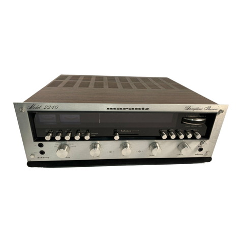
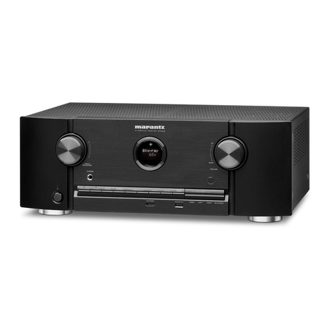
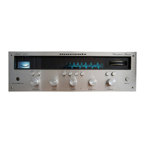
Marantz 2250B User manual


3. AM ALIGNMENT PROCEDURE (~
3.1 AM IF Alignment ( )
1. Connect a sweep generator to the J153 and an alignment scope to the test point B.
2. Rotate each core of IF transformer L153 for maximum height and flat top symmetrical
response.
3.2 AM Frequency Rangeand Tracking Alignment
1. Set AM signal generator to 515 kHz. Turn the tuning capacitor fully closed (place the tuning
pointer at the low end) and adjust the oscillator coil L152 for maximum audio output.
2. Set the signal generator to 1650 kHz. Placethe tuning pointer in the high frequency end and
adjust the oscillator trimmer on the oscillator tuning capacitor for maximum audio output.
3. Repeat steps 1 and 2 until no further adjustment is necessary.
4. Set the generator to 600 kHz and tune the receiver to the same frequency anq adjust a slug
core of AM ferrite rod antenna and RF coil L151 for maximum output.
5. Set the generator to 1400 kHz and tune the receiver to the samefrequency and adjust both
trimming capacitors of antenna and RF tuned circuit for maximum output.
6. Repeat steps 4 and 5 until no further adjustment is necessary.
Note: During tracking alignment reduce the signal generator output as necessaryto avoid AGC
action.
3.3 AM Signal Strength Meter Alignment
Set an AM signal generator to 1000 kHz at 5k1-N, and adjust R178 so that the signal
strength meter may read 90% of the full scale.
,
1
3
4. FM ALIGNMENT PROCEDURE
1. ,Connect an FM signal generator to the FM ANTENNA terminals and an oscilloscope and an
audio distortion analyzer to the TAPE OUTPUT jacks on the rear panel.
2. Set the FM SG to 87 MHz and provide about 3 to 5J.1.V.Placethe tuning pointer at the low
frequency end by rotating the tuning knob and adjust the core of oscillator coil L104 to
obtain maximum audio output.
3. Set the FM SG to 109 MHz and provide about 3 to 5J.1.Voutput. Rotate the tuning knob and
place the tuning pointer at the high frequency end and adjust the trimming capacitor C106
for maximum output.
4. Repeat steps 2 and 3 until no further adjustment is necessary.
5. Set the FM SG to 90 MHz and tune the receiver to the same frequency. Decreasesignal
generator output until the audio output level decreases with the decreasing generator
output. Adjust the antenna coil L101, RF coils L102 and L103 and IF transformer L105 for
minimum audio distortion.
6. Set the FM SG to 106 MHz and tune the receiver to the same frequency. Adjust the trim-
ming capacitor C102, C104 and C105 for minimum distortion.
7. Repeat steps 5 and 6 until no further adjustment is necessary.
8. Adjust the secondary core (upper) of discriminator transformer L201 sothat the center tun-
ing meter pointer indicates its center at no signal applied. Set the FM SG to 98 MHz and
increase its output level I kJ.l.Vand tune the receiver to the samefrequency sothat the center
tuning meter pointer indicates its center.
Adjust the primary core (lower) of L201 for minimum distortion.
9. Set the FM SG to 98 MHz at 1000 kJ.l.V,and adjust R374 so that the signal strength meter
may read 90% ofthe full scale.

5. STEREO SEPARATION ALIGNMENT
1. Set the FM SG to provide I kj.LVat 98 MHz. Tune the receiver to the samefrequency so that
the center tuning meter pointer indicates its center.
2. Turn the FM SG modulation off (with the pilot signal turned off), connect a frequency
counter to test point J310, and adjust R311 so that the frequency counter may precisely
read 19 kHz.
3. Modulate the FM SG with stereo composite signal consisting only of subchannel signal (of
course a pilot signal must be included).
4. Adjust the trimming resistor R301 for maximum and same separation in both channels.
6. MUTING CIRCUIT ALIGNMENT
1. Connect a VTVM across the resistor R363 and adjust the resistor R363 until the meter
reads0.75V DC at no signal.
2. Set the FM SG to provide I kJ1Vat 98 MHz and tune the receiver to the same frequency
correctly.
3. Turn on MUTI NG push switch. Shift the FM signal generator frequency to plus and minus
and note both plus and minus shifted frequencies at which undesirable audio side responses
are muted out. Adjust the R363 so that the same shifted frequencies mute the undesirable
side response.
4. Adjust R362 for proper frequency shift at which the muting circuit operates.
7. DOLBY FM TAPE OUTPUT SETTING
1. Set the modulation of FM SG to 400 Hz, 50% (±37.5 kHz Dev.)
2. Set the FM SG to provide 1 kJ1Vat 98 MHz. Tune the receiver to the same frequency so
that the center tuning meter pointer indicates its center.
3. Turn on DOLBY FM push switch. Set the semifixed resistors RC01 and RC02 so that the
output of the TAPE OUTPUT terminals Rand L become 580 mVat VTVM.
8. AUDIO ADJUSTMENT
1. Voltage adjustment
Connect a DC voltmeter between pin terminal 804 and 805, and adjust the trimming
resistor R806 for 35V DC.
2. Main Amplifier DC off--setalignment
Connect a DC voltmeter with 0.5 or 1 V rangebetween the speakerterminals and adjust the
trimming resistor R707 for "zero" DC output on the meter.
Repeat the sameprocedure for the other channel.
Note: During this alignment no load should be connected to the speakerterminals.
3. Idle-current adjustment
Connect a VTVM between pin terminals 708 and 710. Next, adjust the trimming resistor
R719 sothe VTVM reads10mV DC. Repeat the sameprocedure for the other channel.
4. Check DC off-set voltage aligned in the procedure 2 and if any DC output is observed on the
DC voltmeter, adjust the R707 again for "zero" output.
5. Phono-amplifier adjustment
Connect an oscilloscope to the TAPE OUT jacks and an audio signal generator to the
PHONO jacks. Placethe selector switch in the PHONO position. Increase1 kHz audio signal
gradually until a slight clipping on top of the sine-wave is observed on the oscilloscope.
Adjust the trimming resistor R408 for equal clipping level.
For the other channel adjust R409.
4

:
Figure 1. Dial Stringing
5

COO3
-
J314 <
J305 <
II
J304 .1303 J316 306
J205 (:r-
J:OS J "JSP6 J210
:...-....J --,--
J:;02 -~h
P200
J309
P300
J310
J~ J~9
TI
J317
J318
J320 J319 J1'3 J321 J307
J31lI. T P
r
I
r---
t-----< J308
J322
I
i
JI60
JI" J158:
--
I
,.-J I
I
JU04
1
.--
G
IPUOI ---. r--
IJUOI I I PIOO
0-1--""- JU02 01
FM { 0-1- § ~ [~JI02
!. ~ l~JIC1
7L 0- JUQ3 -r' ;108 ~09
D- 0008 O~ 1I
-r CU02 nIJI" J!~'!50,.J ).J1S2
JI56
IRU04 J~ )- IJ\5.5 157
MUTING t;'" ~
lEVECC- 1 IJU07
IJUO'
cOO2-
AM
>-
Z
<1_
::;;
<I
C~ -
I
-- --
;"06 J404 )--
'" P400
PHONO J405
J«l3 AMP.
tlJ~ --:-
).;c; JCOeJC';02~-
)XC< PCOI JCO' l
~)JC06 J~ I
---- I
I
IN~~
DUBBIN~
JOO'
OU7 ~=:
~
GOO~
~t[b
o0
Ilj]~
~ 0
JT03 ::31 ~
Tor 0-,
,rr02 LTOI
~f-
'-_ JT23A
~FM STOI-1
$TO,-2
$T
+
MONO
MONO
STOr-3
en
+
ON
MUTING
STOf-4
,
+
.2
STOI-'
SOURCE
+
llIPE
PTOI
JT21
T22
6

-
~MOOS
POINTER
+ -
COO. l'~
PRE O\IT IlIAlN IN
I
~~
I~R~
L-H 'J 'T L+-
JOIO
JOV
1
I
-~
LOUDNESS
LOW-FILTER
HI-FILTER
~
~~
--
, SHO'-' +SHOI-2
+$HO'-3
-
re~llii~~~ [
IH--JJ [ti
:1 iI
~
~~'" ..
~" ¥ i~b ~
0:
" 0:
-l3o-
; :3 I" "L--
0: 0: '- -RHI6
8~
~
~
~~
'" 8 ~o ••
0~
~xRHIS
'i 'i'i'i ""
~ ~ "
~'"
ROO4 'i
'i~
L..- _
PYOI FUNCTION LAMP
-I
P200 I
-J205
>-
J~
,
J~ J" J210 ROO
-,
~~
,
,
:--J. ,
:
,
-•••
,
J309 J301J302
J31.5 f-I
I
•........• ~
P300
J314
>-
J310
~-v@
~D~
I
@ ~ 7,
(j]) '-------" 8@®SOOI~3
Jjp4 J<:Q9
r
J203
J3U
rJ317 J305
I
J318
3061
I
J320 J319 J313 "21 J307
J30. "03
J316
~H 1
-
--
- J308
C0CJ2.~r-"1T'- 9JF--
I[0 iJ J207
J '06 >-- J007 1
JIOO 'l' ryJ2O'
JI05 J202
LOO3
'-
JI60
JI03
--
JI6' J'58:
--
PI50
1I
JJ02
JlO'
JI53 Jr5r
JI01
;108 JI09
).,'52
r--
I PIOO
II
Itl
I
-I
I
r:=
I
~;.....
:...--
nJ
Lc"
I
I
I
~U
-
'"~ 0.~ J<:o>-
--- -- !~-Ol)r~
-
~406 J404 >-- I~ 7
·).,.v. P400 ,j,
~~~"-'
·Pore PHONO J405 I
®.£1) ~
·AMP_
J402 -- I
5001-2 9
'~
~
JC08
JC~02 >-.-- tl
04 PCOI
JCOI
---® @-
COO
JCOJ
I~\~
I' i
,j, r;z""'
®19 <I
SOOI-4
flU
lI
~
FOOl
--J,.
r--------;! RE
J027, ,'T1iNd T
FOO3 t~?N~CN..Y~ lGN c( :
,J, ~ .J
J803
J802
JSOl
J804
I
J808 J807 J809 J810 i
P900
POWER
SUPPLY
IJ8C16
I
T20 __
RTOt JT2r
I
PTOI I
[ ~tn RT02
.JT22
.•.•u I
Q?I
STOI-S
SOURCE
+
TAPE
'T17 JTl9
,~
-
-
JTI6
ON .2
STOI-3 STO"O
~F I
+ +
MUTINGMONO
5101-2
ST
+
..:JNO

:
REMOTE
SPEAKER
JOJ5
....,
SPOKE
J("
r--
--0 L
~-o
1--0
- -0 "
-
---'-
r {] L
{]
rD
JOl3
MOOS
-
J703 J704 J,2.!.8
J714 J705
()~,
.- J701 J706
LJ708
J702
L.:::.
J71Q
()HOO2
P700 I
MAIN AMP J711
J712
r~J713
JOlT
J709
"-----,..---- J~
--< ).1713 J705
()~
-70J J706
L.J1'02 J708
P700 ~
IMAIN AMP
J710-<L
J1l1
J7r4
J1J2
J~
J703
J704
J709
-H006
-
oN
r:r RHl5
JOIO
iSHOl- 2 ISHO'-3
J027
coo.
1I
_---.J I
ji
~
IPRE 0lIT MAIN IN
r
L~L~
L-~"~
LOW-FILTER HI-FILTER
--
'5
PEOI
L~~'''''·'
JY01T" JY04l JY05 JY06 JY07 J'l'08
LOUDNESS
~~
tSHO'-'
-,
• H--JJ [t~
""?' JiI
~
,
,,
,~ Cl
I
,I
1"\
,I
~I ~~ 8
~
~
~
;; '!i
~MOO' M002
JYO
TJYOI
I
I
1
I
J808 .#)7 J809 J8l0 i
PYOI FUNCTION LAMP
~ J022
:;J
J021
SOO2
GOO!
r--------,
I [
I ,
L-.J
I(
r----..,
:For CANAOAo:
ICN..Y I
I I
r-\
'C;J
J020
FOOl
i--------:,1 Rf
J027 I ,TON el :
FOO3 ~::'~~~_.JlGN 9 :
,j, ~ __l
J803
J80I
J804
PBOO
POWER
SUPPLY
; J806
I
-
Figure 2. Wiring Diagram
-~

8
_ _ _~ "_r_ •• _~._ •. " .-<-----.-. ..,.•..,.--.- •..-~---- .._ -~,._-,.- - _•.~.--
Model2250B NOTE: This schematic diagram applied to units manufactured for the U.S.A. market.
,
1
'"
·.•.

m applied to units manufactured for the U.S.A. market.
8

"l"O'
"0300>000
wz -177
N:'l:'2.T:l3 1tT~.T05
ril(076319C H'I0000312
2SA763(4,'l 11I'1-13
..-:: ..~.
""2."
I-IT30e7~3e 1'I02OOO22! HT30904~IO HTI073,310 HK(:64919A HI(O~919A
lSC87~E IS247'2 2SC94'Q 2547330 2S04I~p.Q." 2S8~49P,O,R
Figure 3. Schematic Diagram
9

".
JI04
elZ4
OluF
J106
I
I
FUll I
'00 I
I
~
'122
QI",F
Rl06
,.
RIIO
'2'
C1l6
OluF
--------,
""03
HT30~3~18
2SC~3~8 ,
,
CI19
rw' C,~ ~~~F >6V
II I 20PF
--~
IRloa
21K
RIO? TIe1l7
41'1( O''JF
I
R/~l :
I
-- -----.,
CIOI I
,
I
I
I
~I03 CI03 cr09
rOOt( ~PF
,
I ClIO
I roooPF
I
I
IRIOI
I ~61(
•... ----
r;o~---:~~~~;'>A-
IFM FRONT END ~2S,~19Y C',.
IL,a,
I
I
L
J102
Figure 9. FM Front End (P100) Schematic Diagram
,~
Figure 10. FM Front End (PlOD) Component Locations
14
I
j
-,

J'61
-,I
I
I
I
I
_...J
~,~~
HHOO00212
31027
1-41 ~3 . I ~4
HTI04942A
25A494Y, G
";!~2
HT313272A
25CI3275,T
MI'I
HCIOOO~06
jJPC30C
L
r-P150-
IAM Tl,NER
I
I
I
I
,",,7
Figure 11. AM Tuner (P150) Schematic Diagram
Figure 12. AM Tuner (P150) Component Locations
15

e-)
I
=t:::1I
I
I
I
Figure 13. FM IF (P200) Schematic Diagram
Figure 14. FM IF (P200) Component Locations
•
r---
I
I
_-.J
r------------------------------
P200 .Uor .••.••lor ""'. Hl'O_11'.2'8,/IV.11"1, 11"'.1111I.1/' ••••'6.11'.J10.1 ••,.II~.n'./2e,n'l ••,.to. lJ', 111 --,
IFM IF AMP HT308291C (25C829C) HT30~44tB(lSC644S) HDIOOOrO~ IIN60) H0200110~ (ISI~'~) HOlOOO]OZ (20A90M) I
Il)IV H204 - ~"'206 H207 'U1II4 Allll~I'UloffillOl "Ih~nl Ill). ~~'; ~~ .,v CllO Hl,e '1'0' ,101 "IJO 820 IVol I~,)' ]lll .v _ "0 ~ " •.•••..•..• '11 ~02'" 1'0 44'" lI~rl
J2'O, czoe 1'". nA14' rIt..... Ill!!) It (IH UK/PI I
t0161 •• ,'0 _ ... . CUt t'O t,O "0 .,. 01" ~~ T .•. :~e'
&J
en

r-~=-- IU~lC:--
HF2003CIC ••30 •••••'" '03"_3"
I2Sk30T HT)08Z810
a,. 25C8285
Figure 15. FM MPX (P300) Schematic Diagram
17
Figure 16. FM MPX (P300) Component Locations

.
JC04
I
,:C05
JC08
I
.IC06
I
Jcor
CC03
,.'
.•. 2~\I
ce04
'.F I
CC02 2'"
I ~~\.He02 14 OV
RC04 JL....:.a~ _
peol
DOLBY FM OUT
r----~Ol Heoz
HBI3272A
I2SC1327S,T
IRC03
..'
JCOI
Figure 17. Dolby FM Assembly (peDl) Schematic Diagram
Figure 18. Dolby FM Assembly (PCD1) Component locations

J40~
I
:.J
Coil01
,PF
l't407. 408
HD2DOOl21
IS- 2473C v.
H403. 404
HT313442A
2SCI344D,E
r~=.4-;;;-
IHT313441E
2SCI344E
I
I
JOO'
P400
LP~O~P _
J402
I
I
J403
Figure 19. Phono Amplifier (P400) Schematic Diagram
Figure 20. Phono Amplifier (P400) Component locations
I;
19

no,
.)1'0.
J710
J711
'H35
'0 ';712
C710 .ljoiF J113
IPoe
6.81(
7V
~704 R705
II( 100 t.:::.J
H7'04
P700
MAIN AMP,
R1'03
• OK
cro,
133"
,"vC102
;01"
I'"
+
I_ro, IJ702
r
I
I
I
Jro,
Figure 21. Main Amplifier (P700) Schematic Diagram
G.~-F06
J:!P8:;
~oV'~
J:~t:·
J710
.1711J1l2..
G' ~.!j! G
1!1
~,'
G
~.
'. ".
~.:
Figure 22. Main Amplifier (P700) Component Locations
20

J002
-- -JOO'
.:sIO I
JOO'
J~
~a06
,..
coO<
.• 22"F
>ov
H804
H803
7.0\1
3~ cv
I
I
I
.1803
r------
H808 Q8Cl HeOI
r- - -, 10 44 :)v
~J'O'!r' ~ri V/i
ca:c IIat ••'.. I
,
Figure 23. Power Supply (P800) Schematic Diagram
Figure 24. Power Supply (P800) Component Locations
,
,
21

r
W----,"CO., (0. I
HTI01212A
ZSA 121S, T I
I
I
I
I
I
I
I
II
I
-----~
Figure 25. Pre Tone Amplifier (PEOn Schematic Diagram
Figure 26. Pre Tone Amplifier (PEOn Component locations

Q--------------..,
PHO I .~(U \._. "\U,, ••, .• 'I..T(. "A'" .(-.;IT1[ I
FILTER. SP. ,..eo. , ,10(1'.' 1••0' - J'''0'·. poo··, .•••'1
Figure 27. Filter (PH01) Schematic Diagram
RH16
--'#N-.
RH15
.~.
JH13 JH18 JH12 JH16
0000
SHOl-5
·,'~:':
· ~..
:
• lit •
.
Figure 28. Filter (PH01) Component Locations
Figure 29. Monitor (PT01) Schematic Diagram
23
8Hl>e ~2-A\lU:J
Figure 30. Monitor (PT01) Component Locations
Other manuals for 2250B
2
Table of contents
Other Marantz Stereo Receiver manuals

Marantz
Marantz SR5015 DAB User manual

Marantz
Marantz SR4120 User manual

Marantz
Marantz SR6011 User manual

Marantz
Marantz SR7007 User manual

Marantz
Marantz SR5006 User manual

Marantz
Marantz SR5010 User manual

Marantz
Marantz SR7200 User manual

Marantz
Marantz NR1609 User manual

Marantz
Marantz 2325 User manual

Marantz
Marantz NR1200 User manual

Marantz
Marantz 2252 User manual

Marantz
Marantz NR1710 User manual

Marantz
Marantz 2275 User manual

Marantz
Marantz 2238 User manual

Marantz
Marantz SR-19EX User manual

Marantz
Marantz 2330B User manual

Marantz
Marantz SR6013 User manual

Marantz
Marantz SR5300 User manual

Marantz
Marantz SR5500 User manual

Marantz
Marantz 2275 User manual