MEIG SLM500 Guide

MeiG Smart product technical information
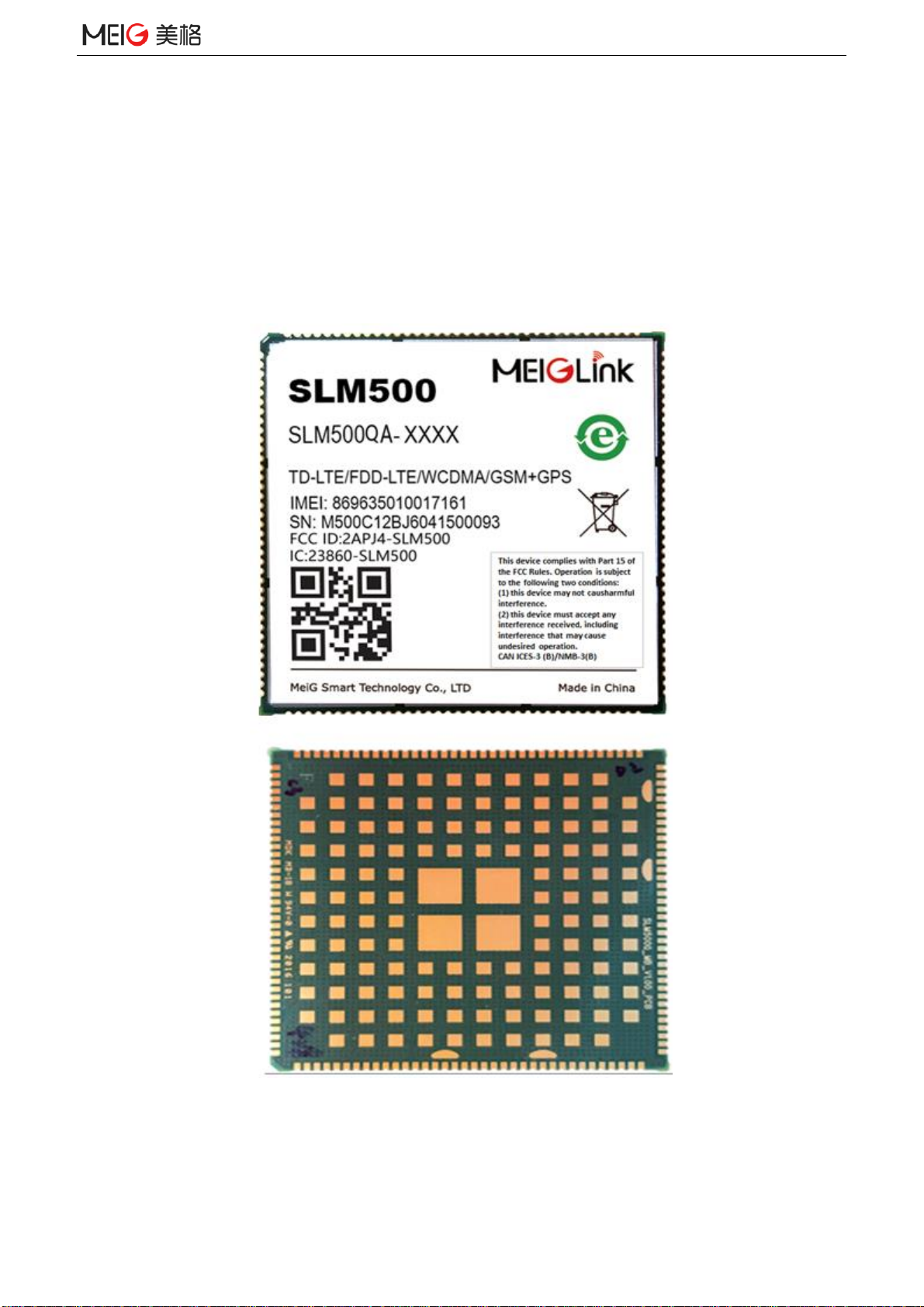
SLM500 Hardware Design Guide Page 1
SLM500 Hardware Design Guide
Released Date: 2020/07
File name: SLM500 Hardware Design Guide
Version Number: V1.00
Company: MeiG Smart Technology Co., Ltd

MeiG Smart product technical information
SLM500 Hardware Design Guide Page 2
IMPORTANT NOTICE
COPYRIGHT NOTICE
Copyright © MeiG Smart Technology Co., Ltd. All rights reserved.
All contents of this manual are exclusively owned by MeiG Smart Technology Co., Ltd(MeiG Smart
for short), which is under the protection of Chineselawsandcopyrightlaws in international conventions.
Anyone shall not copy, spread, distribute, modify or use in other ways with its contents without the
written authorization of MeiG Smart. Those whoviolatedwillbe investigated by corresponding legal
liability in accordance with the law.
NO GUARANTEE
MeiG Smart makes no representation or warranty, either express or implied, for any content in this
document, and will not be liable for any specific merchantability and applicable or any
indirect,particular and collateral damage.
CONFIDENTIALITY
All information contained here (including any attachments) is confidential. The recipient
acknowledges the confidentiality of this document, and except for the specific purpose, this document
shall not be disclosed to any third party.
DISCLAIMER
MeiG Smart will not take any responsibility for any property and health damage caused by the
abnormal operation of customers. Please develop the product according to the technical specification
and designing reference guide which defined in the product manual. MeiG Smart have the right to
modify the document according to technical requirement with no announcement to the customer.
MeiG Smart product technical information
SLM500 Hardware Design Guide Page 3
SLM500 Hardware Design Guide_V1.00

MeiG Smart product technical information
SLM500 Hardware Design Guide Page 4
Foreword
Thank you for using the SLM500 module from Meg Smart. This product can provide data
communication services. Please read the user manual carefully before use, you will appreciate its
perfect function and simple operation method.
The company does not assume responsibility for property damage or personal injury caused by
improper operation of the user. Users are requested to develop the corresponding products according
to the technical specifications and reference designs in the manual. Also pay attention to the general
safety issues that mobile products should focus on.
Before the announcement, the company has the right to modify the contents of this manual according
to the needs of technological development.

MeiG Smart product technical information
SLM500 Hardware Design Guide Page 5
Contents
1. Introduction.......................................................................................................................................................... 8
2. Module overview.................................................................................................................................................. 8
2.1 Summary of features...................................................................................................................................... 9
2.2 Block diagram..............................................................................................................................................11
3. Module Package..................................................................................................................................................... 12
3.1.Pin distribution diagram............................................................................................................................. 12
3.2. Pin definitions.............................................................................................................................................. 13
3.3. Mechanical Dimensions.............................................................................................................................. 27
4. Interface application.............................................................................................................................................. 29
4.1. Power Supply.............................................................................................................................................. 29
4.1.1. Power Pin................................................................................................................................................. 31
4.2. Power on and off......................................................................................................................................... 31
4.2.1. Module Boot............................................................................................................................................. 31
4.2.2. Module Shutdown.................................................................................................................................... 33
4.2.2.1 PWRKEY Shutdown............................................................................................................................. 33
4.2.3.Module Reset............................................................................................................................................. 33
4.3. VCOIN Power............................................................................................................................................. 34
4.4. Power Output.............................................................................................................................................. 35
4.5. Serial Port.................................................................................................................................................... 35
4.6. MIPI Interface............................................................................................................................................. 37
4.6.1. LCD Interface .......................................................................................................................................... 38
4.6.2.MIPI Camera Interface........................................................................................................................... 40
4.7.CapacitiveTouch Interface.......................................................................................................................... 43
4.8.Audio Interface ............................................................................................................................................ 44
4.8.1Receiver Interface Circuit ......................................................................................................................... 44
4.8.2 Microphone receiving Circuit ................................................................................................................. 45
4.8.3.Headphone Interface Circuit ................................................................................................................... 45
4.8.4.Speaker Interface Circuit......................................................................................................................... 46
4.8.5.I2S Interface .............................................................................................................................................. 46
4.9. USB Interface.............................................................................................................................................. 46
4.9.1. USB OTG.................................................................................................................................................. 47
4.10. Charging Interface.................................................................................................................................... 48
4.10.1. Charging Detection................................................................................................................................ 49
4.10.2. Charge Control ...................................................................................................................................... 49
4.10.3. BAT_CON_TEM................................................................................................................................... 49
4.11 UIM Card Interface................................................................................................................................... 49
4.12. SD Card Interface..................................................................................................................................... 50
4.13 I2C Bus Interface....................................................................................................................................... 51
4.14 Analog to Digital Converter (ADC).......................................................................................................... 51
4.15. PWM.......................................................................................................................................................... 51
4.16. Motor ......................................................................................................................................................... 52
4.17 Antenna Interface...................................................................................................................................... 52
4.17.1 Main Antenna.......................................................................................................................................... 52
4.17.2 DRX Antenna.......................................................................................................................................... 53
4.18.3 GPS Antenna........................................................................................................................................... 54
4.18.4 WiFi/BT antenna..................................................................................................................................... 55
5.PCB Layout............................................................................................................................................................. 56
5.1. Module PIN distribution............................................................................................................................ 56
5.2. PCB Layout Principles............................................................................................................................... 56
5.2.1. Antenna..................................................................................................................................................... 56
5.2.2 Power Supply............................................................................................................................................. 57
5.2.3. SIM Card.................................................................................................................................................. 57
5.2.4. MIPI.......................................................................................................................................................... 58
5.2.5. USB............................................................................................................................................................ 58
5.2.6.Audio.......................................................................................................................................................... 58
5.2.7. Other......................................................................................................................................................... 59
6. Electrical, Reliability............................................................................................................................................. 61
6.1 Absolute Maximum...................................................................................................................................... 61
6.2 Working Temperature................................................................................................................................. 61

MeiG Smart product technical information
SLM500 Hardware Design Guide Page 6
6.3 Working Voltage.......................................................................................................................................... 61
6.4 Digital Interface Features............................................................................................................................ 61
6.5 SIM_VDD Characteristics .......................................................................................................................... 62
6.6 PWRKEY Feature....................................................................................................................................... 62
6.7 VCOIN Feature............................................................................................................................................ 62
6.8 Current Consumption (VBAT = 3.8V)....................................................................................................... 62
6.9 Electrostatic Protection............................................................................................................................... 63
6.10 Module Operating Frequency Band......................................................................................................... 63
6.11 RF Characteristics..................................................................................................................................... 64
6.12 Module Conduction Receiving Sensitivity............................................................................................... 64
6.13 WIFI Main RF Performance .................................................................................................................... 66
6.14 BT Main RF Prformance .......................................................................................................................... 67
6.15 GNSS Main RF Performance ................................................................................................................... 67
7. Production.............................................................................................................................................................. 68
7.1. Top And Bottom Views Of The Module ................................................................................................... 68
7.2. Recommended Soldering Furnace Temperature Curve ......................................................................... 69
............................................................................................................................................................................. 69
7.3. Humidity Sensitivity (MSL)....................................................................................................................... 69
7.4. Baking Requirements................................................................................................................................. 70
8. Support Peripheral Device List............................................................................................................................ 71
9. Appendix ................................................................................................................................................................ 72
9.1. Related Documents..................................................................................................................................... 72
9.2. Terms And Explanations............................................................................................................................ 72
9.3. Multiplexing function................................................................................................................................. 77
9.4. Safety Warning ........................................................................................................................................... 77

MeiG Smart product technical information
SLM500 Hardware Design Guide Page 7
Version History
Date
Version
Change description
Author
2020-07-02
1.00
First edition
MeiG Hardware

MeiG Smart product technical information
SLM500 Hardware Design Guide Page 8
1.Introduction
This document describes the hardware application interface of the module, including the
connection of the circuit and the RF interface. It can help users quickly understand the interface
definition, electrical performance, and structural dimensions of the module. Combining this
document with other application documents, users can quickly use modules to design mobile
communication applications.
2.Module overview
SLM500 module uses the Qualcomm solution based on arm cotex-A53 four core processor,
with the highest main frequency of 4 * 1.3GHz, and the memory supports single channel 32-bit
LPDDR3/672MHz.This module is suitable for broadband intelligent wireless communication
modules of TD-LTE/FDD-LTE/WCDMA/EVDO/TD-SCDMA/CDMA/GSM network
standards.
The physical interface of the module is a 272-pin pad that provides the following hardware
interfaces:
Three 1.8V UART serial ports, supporting four or two wires.
Main LCD(MIPI interface).
Two groups of Camera interface(MIPI data).
USB2.0 interface.
Three groups of Audio input interface.
Three groups of Audio output interface.
Dual-Sim card interface.
GPIO interface.
Five groups of I2C interfaces.
One sets of SPI interfaces.
TF card interface.
Support GNSS,WiFi,Bluetooth 4.2
MeiG Smart product technical information
SLM500 Hardware Design Guide Page 9
2.1 Summary of features
Table 2.1:SLM500 features
Product characteristics
Description
CPU
Quad-core A53 (64bit) 1.3GHz
GPU
Adreno 308 @485MHz
System memory
8GB eMMC + 1GB LPDDR3 compatible with 16GB+2GB
OS
Android 10
Size
40.5x40.5x2.8mm,LCC 146pin+LGA 128pin
RF band--
SLM500A
FDD-LTE: B2/4/5/7/12/13/17/25/26/66
WCDMA: B2/4/5
GSM: B2/5
Wi-Fi
IEEE 802.11b/g/n 2.4G 802.11a/n 5G
Bluetooth
BT 4.2
FM
No support
GNSS
GPS/ Beidou/ Glonass
Data
Acces
s
TD-LTE
Cat4 TD-LTE 117/30Mbps
FDD-LTE
Cat4 FDD-LTE 150/50Mbps
DC-HSPA+
42/11.2Mbps
TD-HSPA
2.8/2.3Mbps
EVDO
Rev.A
3.1/1.8Mbps
EDGE
Class12, 236.8kbps/236.8kbps
GPRS
Class12, 85.6kbps/85.6kbps
SIM
DSDS(Dual Sim & Dual Stanby)
3.0/1.8V
Support SIM hot plug
L/W/G+G with CSFB to W/G
L/TDS/G+G with CSFB to TDS/G
L/EVDO/CDMA1X+ G
L/W/TDS/G+CDMA1X
Don’t support dual CDMA SIM card
Display
Matrix:
HD+:1440*720 60fps
LCD Size: User defined
Interface: One MIPI DSI 4-lane;
Camera
(Front and Rear)
Interface: main: MIPI CSI 4-lanes; front: MIPI CSI 4-lanes
Camera Pixel: Max. Rear 5Mp/Front up to 13Mp
Video
decode
1080p 30 fps: H.264/VP8/HEVC (H.265) 720p 30fps in
SW
Video
encode
1080p 30 fps: H.264
MeiG Smart product technical information
SLM500 Hardware Design Guide Page 10
Input Device
Key(Power on/off, Reset , Home, Volume+, Volume-)
Capacitive TP
Reset
Support HW reset
Application interface
Interface
name
Main function description
VBAT
4pin,Power input,3.4V~4.2V,Nominal
value3.8V
SDIO *1
TF Card,Support 32GB max
USB
Support OTG
USB_BOOT(Force USB boot for emergency
downloads)
BLSP ports
6 ports(BLSP2-7), 4-bits each, multiplexed serial
interface functions
UART*3
Max up to 4 Mbps
I2C*5
Support
SPI
(master only)
Support
ADC*1
Support
PWM*1
Support
Charge
Max up to 1.44A
Vibrator
Support
GPIO
40 GPIOs,Excluded BLSP multiplexing GPIO.
VCOIN
Real time clock backup battery
RF Interface
Multimode LTE main antenna
Multimode LTE diversity antenna
The GPS antenna
2.4G +5G WiFi/BT antenna
Audio
One main MIC
One noise reduction MIC
One Handsfree speaker.
One earpiece
One stereo headphone.
Accessories versions
SLM500QW_MB_V1.01_PCB
Software versions
SLM500Q_EQ000_2774.2AAF2F74.BCA2CDE_200628_100_V01_T09
MeiG Smart product technical information
SLM500 Hardware Design Guide Page 11
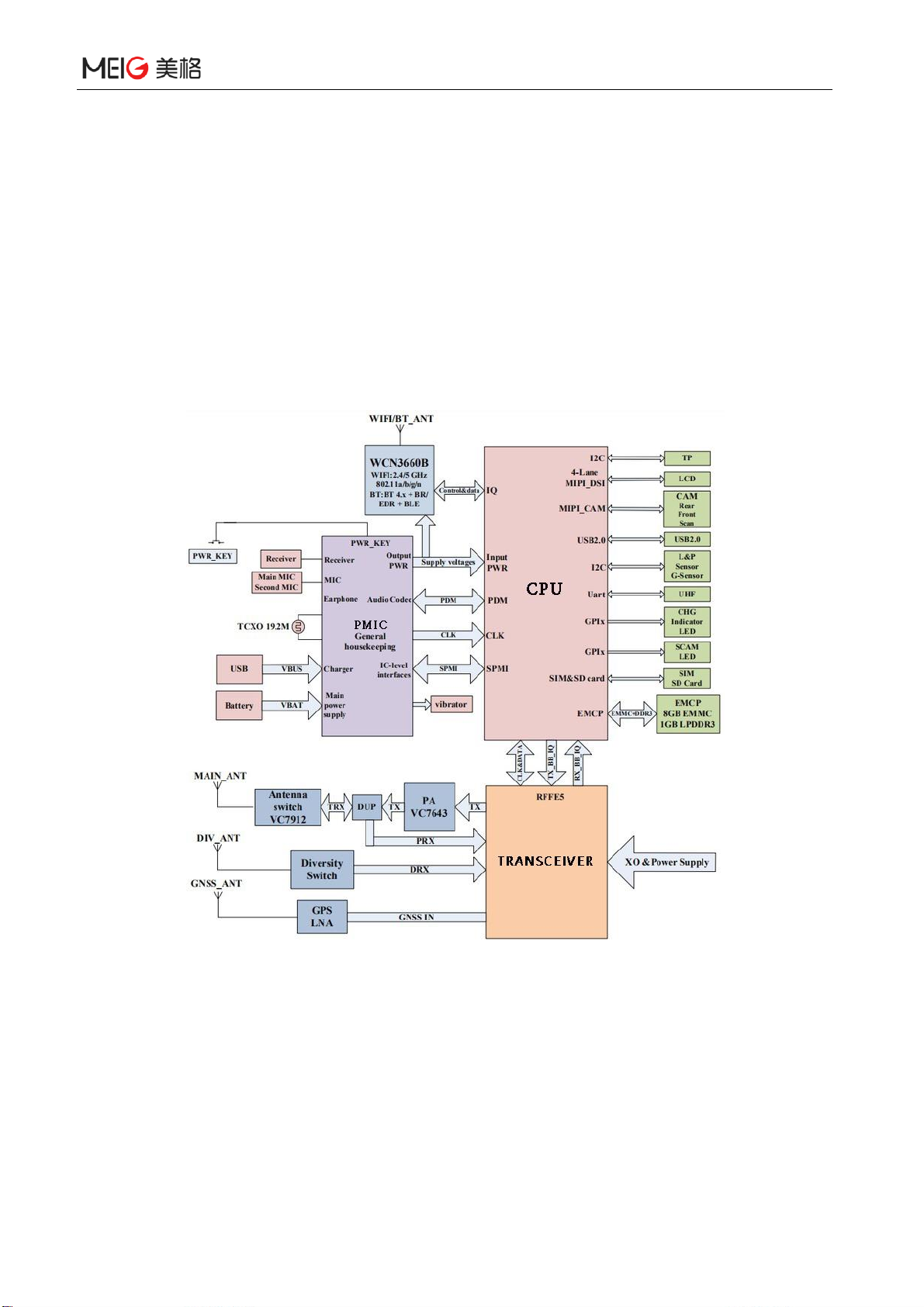
2.2 Block diagram
The following figure lists the main functional parts of the module:
baseband chip
power management chip
Transceiver chip
WCN3660-WIFI/BT Two in one chip
Antenna interface
LCD/CAM-MIPI interface
EMCP memory chip
AUDIO interface
UART、SD card interface,SIM card interface,I2Cinterface,etc.
Figure 2.1: module function block diagram

MeiG Smart product technical information
SLM500 Hardware Design Guide Page 12
3. Module Package
3.1.Pin distribution diagram
Figure 3.1:module pin diagram (top view)

MeiG Smart product technical information
SLM500 Hardware Design Guide Page 13
3.2. Pin definitions
table 3.1:Pin description
Pin number
Pin number
I/O
Description
Comment
The power supply
VBAT
1、2、145、146
I
The module provides Four
VBAT power pin pins. The
SLM500 operates from a single
supply with a voltage range
from 3.4V to 4.2V for VBAT.
Externally,
large capacito-
rs and Zener
diodes must be
added for
surge protec-
tion.
VBUS
141、142
I/O
5V charging input power.
VCOIN
126
I/O
When the VBAT of the system
power is absent, the external
backup battery provides power
to the system real-time clock.
When VBAT is present, the
backup battery is charged.
VCOIN pins
connect 3V
button batteries
or large
capacitors.
VREG_L5_1P8
111
O
1.8V power output, Power
supply always available for IO
port pull-up and level conver-
sion, not for peripheral power
supply
50mA
VREG_L6_1P8
125
O
1.8 V power output, standby will
be closed, used for Camera,
LCD and other small current
power supply.
100mA
VREG_L10_2P8
156
O
2.8V power output, used for
Sensor, TP power supply.
150mA
VREG_L17_2P85
129
O
2.85 V power output, for LCD,
Camera 2.8V.
300mA
VREG_L11_SDC
38
O
TF card power supply pin
500mA
VREG_L12_ SDC
32
O
TF card signal pull-up power
supply pin
50mA
VREG_L14_UIM1
26
O
UIM power supply pins
50mA
VREG_L15_UIM2
21
O
UIM power supply pins
50mA
VREG_L16_AVDD
193
O
Camera AVDD
50mA
GND
3、7、12、15、
27、51、62、69、
76、78、85、86、
88、89、120、
122、130、132、
135、140、143、
144、149、162 、
171、172、176 、
187~191、202~204
206~224、226~231
233~238、240、
241、243、244、
245、247、248、
GND

MeiG Smart product technical information
SLM500 Hardware Design Guide Page 14
250、251、255、
256、258、259、
261、266、268、
269、271~274
display interface (MIPI)
MIPI_DSI0_CLK_M
52
I/O
MIPI_LCD clock
MIPI_DSI0_CLK_P
53
I/O
MIPI_DSI0_LANE0_M
54
I/O
MIPI_LCD data
MIPI_DSI0_LANE0_P
55
I/O
MIPI_DSI0_LANE1_M
56
I/O
MIPI_DSI0_LANE1_P
57
I/O
MIPI_DSI0_LANE2_M
58
I/O
MIPI_DSI0_LANE2_P
59
I/O
MIPI_DSI0_LANE3_M
60
I/O
MIPI_DSI0_LANE3_P
61
I/O
GPIO61_LCD_RST_N
49
O
LCD reset
GPIO24_LCD_TE0
50
I/O
LCD frame sync signal
UART(1.8V)
GPIO0_UART1_TXD
154
I
UART1 data transmit
GPIO1_UART1_RXD
153
O
UART1 data receive
GPIO4_DBG_UART_TX
94
I
UART2 data receive
GPIO5_DBG_UART_RX
93
O
UART2 data transmit
GPIO16_UART5_TXD
34
I
UART5 data receive
GPIO17_UART5_RXD
35
O
UART5 data transmit
GPIO18_UART5_CTS
36
I
UART5 Clear To Send(CTS)
GPIO19_UART5_RTS
37
O
UART5 Request To Send
(RTS)
UIM card Interface
GPIO54_UIM1_DET
22
I
UIM1 insert detect
UIM1_RESET
23
O
UIM1 reset
UIM1_CLK
24
O
UIM1 clock
UIM1_DATA
25
I/O
UIM1 data
GPIO58_UIM2_DET
17
I
UIM2 insert detect
UIM2_RESET
18
O
UIM2 reset
UIM2_CLK
19
O
UIM2 clock
UIM2_DATA
20
I/O
UIM2 data
Front Camera

MeiG Smart product technical information
SLM500 Hardware Design Guide Page 15
MIPI_CSI0_CLK_M
157
I/O
Front Camera MIPI clock
MIPI_CSI0_CLK_P
196
I/O
MIPI_CSI0_LANE0_M
158
I/O
Front Camera MIPI data
MIPI_CSI0_LANE0_P
197
I/O
MIPI_CSI0_LANE1_M
159
I/O
MIPI_CSI0_LANE1_P
198
I/O
MIPI_CSI0_LANE2_M
160
I/O
MIPI_CSI0_LANE2_P
199
I/O
MIPI_CSI0_LANE3_M
161
I/O
MIPI_CSI0_LANE3_P
200
I/O
GPIO28_SCAM_MCLK2
75
I/O
Front Camera main clock
GPIO129_SCAM_RST_N
81
I/O
Front Camera reset
GPIO125_SCAM_PWDN
82
I/O
Front Camera dormancy
Rear Camera
MIPI_CSI1_CLK_M
63
I/O
Rear Camera MIPI clock
MIPI_CSI1_CLK_P
64
I/O
MIPI_CSI1_LANE0_M
65
I/O
Rear Camera MIPI data
MIPI_CSI1_LANE0_P
66
I/O
MIPI_CSI1_LANE1_M
67
I/O
MIPI_CSI1_LANE1_P
68
I/O
MIPI_CSI1_LANE2_M
72
I/O
MIPI_CSI1_LANE2_P
73
I/O
MIPI_CSI1_LANE3_M
70
I/O
MIPI_CSI1_LANE3_P
71
I/O
GPIO26_MCAM_MCLK0
74
I/O
Rear Camera main clock
GPIO128_MCAM_RST_N
79
I/O
Rear Camera reset
GPIO126_MCAM_PWDN
80
I/O
Rear Camera dormancy
Audio Interface
MIC_GND
5
The main MIC negative
MIC_IN1_P
4
I
The main MIC positive
MIC_IN2_P
6
I
Headphone MIC positive
MIC_IN3_P
148
I
Secondary MIC positive
MIC_BIAS1
147
O
The BIAS voltage of main MIC
is used in the design of silicon
wheat
MIC_BIAS2
155
O
The BIAS voltage of the
earphone MIC is used in the
design of silicon wheat
MeiG Smart product technical information
SLM500 Hardware Design Guide Page 16
CDC_HPH_R
136
O
Right channel of earphone
CDC_HPH_L
138
O
Left channel of earphone
CDC_HSDET_L
139
I
Headphone plug and unplug
detection
CDC_HPH_REF
137
I
Earphone reference GND
EAR_P
8
O
Earpiece output negative
EAR_M
9
O
Earpiece output positive
SPKR_OUT_P
10
O
Power amplifier output negative
Class D
SPKR_OUT_M
11
O
Power amplifier output positive
Class D
SD card Interface
GPIO67_SD_CARD_DET_N
45
I/O
SD card insertion detection
SDC2_SDCARD_CMD
40
I/O
SD CMD
SDC2_SDCARD_CLK
39
I/O
SD clock
SDC2_SDCARD_D0
41
I/O
SD data
SDC2_SDCARD_D1
42
I/O
SDC2_SDCARD_D2
43
I/O
SDC2_SDCARD_D3
44
I/O
I2C
GPIO29_CAM_I2C_SDA0
84
I/O
Special I2C signal can only be
used for CAM
Pullup to
VREG_L6_1P
8
GPIO30_CAM_I2C_SCL0
83
I/O
GPIO31_DCAM_I2C_SDA1
205
I/O
Default for DCAM
GPIO32_DCAM_I2C_SCL1
166
I/O
GPIO14_SENSOR_I2C4_SDA
92
I/O
Special I2C signal can only be
used for SENSOR
GPIO15_SENSOR_I2C4_SCL
91
I/O
GPIO10_TP_I2C3_SDA
48
I/O
Universal I2C signal, which is
used by default for TP
Pullup to
VREG_L5_1P
8
GPIO11_TP_I2C3_SCL
47
I/O
GPIO6
167
I/O
Universal I2C signal,。
GPIO7
168
I/O
TP
GPIO10_TP_I2C3_SDA
48
I/O
Universal I2C signal, which is
used by default for TP
Pullup to
VREG_L5_1P
8
GPIO11_TP_I2C3_SCL
47
I/O
GPIO65_TP_INT_N
30
I
TP interrupt
GPIO64_TP_RESET_N
31
O
TP reset
USB
USB_HS_DM
13
I/O
USB DM
USB_HS_DP
14
I/O
USB DP
USB_HS_ID
16
I
USB ID

MeiG Smart product technical information
SLM500 Hardware Design Guide Page 17
Antenna interface
RF_MAIN
87
I/O
The main antenna
RF_WIFI/BT
77
I/O
WIFI/BT antenna
RF_DIV
131
I
Diversity antenna
RF_GPS
121
I
GPS antenna
GPIOand default function
GPIO20
119
I/O
Generic GPIO, SPI MOSI
GPIO21
118
I/O
Generic GPIO, SPI MISO
GPIO22
117
I/O
Generic GPIO, SPI CS
GPIO23
116
I/O
Generic GPIO, SPI CLK
GPIO89
115
I/O
Generic GPIO, without default
configuration
GPIO44_MAG_INT
109
I/O
The default configuration is the
compass interrupt signal.
GPIO42_ACCL_INT_N
110
I/O
The default configuration is G-
sensor interrupt
GPIO43_ALSP_INT_N
107
I/O
The default configuration is Ps-
sensor interrupt signal
GPIO63_GYRO_INT
108
I/O
The default configuration is the
gyroscope interrupt signal.
GPIO34
170
I/O
Generic GPIO, without default
configuration
GPIO85
265
I/O
Generic GPIO, MI2S1 SCK
GPIO86
239
I/O
Generic GPIO, MI2S1 D1
GPIO87
105
I/O
Generic GPIO, MI2S1 WS
GPIO88
264
I/O
Generic GPIO, MI2S1 D0
GPIO32_DCAM_I2C_SCL1
166
I/O
default configuration Depth
camera I2C
GPIO31_DCAM_I2C_SDA1
205
I/O
default configuration Depth
camera I2C
GPIO27_DCAM_MCLK
165
I/O
default configuration Depth
camera MCLK
GPIO38_DCAM_RST
164
I/O
default configuration Depth
camera reset
GPIO41_DCAM_PWDN
163
I/O
default configuration Depth
camera power down
GPIO12
101
I/O
General purpose GPIO, no
default configuration
GPIO48
99
I/O
Generic GPIO, without default
configuration
GPIO59
100
I/O
Generic GPIO, without default
configuration
GPIO13
102
I/O
Generic GPIO, without default
configuration
GPIO61
267
I/O
Generic GPIO, without default
configuration

MeiG Smart product technical information
SLM500 Hardware Design Guide Page 18
GPIO45
98
I/O
Generic GPIO, without default
configuration
GPIO25
90
I/O
Generic GPIO, without default
configuration
GPIO33
33
I/O
Generic GPIO, without default
configuration
GPIO39
201
I/O
Generic GPIO, without default
configuration
GPIO46
113
I/O
Generic GPIO, without default
configuration
GPIO47
124
I/O
Generic GPIO, without default
configuration
GPIO62
123
I/O
Generic GPIO, without default
configuration
GPIO66
106
I/O
Generic GPIO, without default
configuration
GPIO90
177
I/O
Generic GPIO, without default
configuration
GPIO93
112
I/O
Generic GPIO, without default
configuration
GPIO94
104
I/O
Generic GPIO, without default
configuration
GPIO95
103
I/O
Generic GPIO, without default
configuration
GPIO127
169
I/O
Generic GPIO, without default
configuration
GPIO25
90
I/O
Generic GPIO, without default
configuration
GPIO130
97
I/O
Generic GPIO, without default
configuration
GPIO104_RFFE3_CLK
260
I/O
GRFC only used for RF Tuner,
control,not for general GPIO
GPIO106_RFFE3_DATA
262
I/O
GNSS_LNA_EN
194
I/O
External GPS LNA enable
Other functional pin
FORCED_USB_BOOT
46
I
Pull up to 1.8 V into the
emergency download mode
CHARGE_SEL
127
I
SMB1360 (external charge IC)
is used, the pin shall be
grounded; when PM215is used,
the pin shall be suspended.
CHG_LED
195
O
The charging indicator light
negative
GPIO91_KEY_VOL_UP_N
95
I/O
Control volume increase
GPIO50_KEY_VOL_DOWN
96
I/O
Control volume decrease
KYPD_PWR_N
114
I
Pull down to power on / off
RESET_N
225
I
Pull down to reset
BATT_THERM
134
I
Battery temperature detection,
Battery terminal NTC resistance
default 47K).

MeiG Smart product technical information
SLM500 Hardware Design Guide Page 19
VBAT_SNS_P
133
I
Battery voltage monitoring
PM_VIB_DRV_N
28
O
Motor negative control
ADC
128
I
Analog voltage input can be
used as ADC input
PWM
29
O
Analog voltage input can be
used as PWM input
optional
NFC_CLK
181
O
NFC Clock
NFC_CLK_REQ
182
I
Default PM215 GPIO2
CBL_PWR_N
186
I
Grounding support power on
automatic startup
BAT_ID
185
I
Battery type detection
RESERVED
150、151、152、
173、174、175、
178、179、180、
183、184、192、
232、242、246、
249、252、253、
254、257、263、
270
Table 3.2:Pin Characteristics
PIN#
SLM500 Pin name
GPIO
Interrupt
Pad
characteristics
Functional description
1
VBAT
PI,PO
Battery,3.5V-4.2V,default 3.8V
2
VBAT
PI,PO
Battery,3.5V-4.2V,default 3.8V
3
GND
GND
GND
4
MIC_IN1_P
AI
Microphone 1 input plus
5
MIC_GND
GND
Microphone bias filter ground
6
MIC_IN2_P
AI
Microphone 2 input plus
7
GND
GND
GND
8
EAR_P
AO
Earpiece output, plus
9
EAR_M
AO
Earpiece output, minus
10
SPKR_OUT_P
AO
Class-D speaker driver output, plus
11
SPKR_OUT_M
AO
Class-D speaker driver output, minus
12
GND
GND
GND
13
USB_HS_DM
AI,AO
USB data minus
14
USB_HS_DP
AI,AO
USB data plus
15
GND
GND
GND
MeiG Smart product technical information
SLM500 Hardware Design Guide Page 20
16
USB_HS_ID
AI
USB ID
17
GPIO58_UIM2_DET
GPIO58*
B-PD:nppukp
Configurable I/O,UIM2 removal detection
18
UIM2_RESET
GPIO57
B-PD:nppukp
Configurable I/O,UIM2 reset
19
UIM2_CLK
GPIO56
B-PD:nppukp
Configurable I/O,UIM2 clock
20
UIM2_DATA
GPIO55
B-PD:nppukp
Configurable I/O,UIM2 data
21
VREG_L15_UIM2
PO
PMIC output for UIM2
22
GPIO54_UIM1_DET
GPIO54*
B-PD:nppukp
Configurable I/O,UIM1 removal detection
23
UIM1_RESET
GPIO53
B-PD:nppukp
Configurable I/O,UIM1 reset
24
UIM1_CLK
GPIO52
B-PD:nppukp
Configurable I/O,UIM1 clock
25
UIM1_DATA
GPIO51
B-PD:nppukp
Configurable I/O,UIM1 data
26
VREG_L14_UIM1
PO
PMIC output for UIM1
27
GND
GND
GND
28
PM_VIB_DRV_N
PI
Haptics driver output negative
29
PWM
AO-Z,DI,DO
Configurable MPP,PWM,ADC
30
GPIO65_TP_INT_N
GPIO65*
B-PD:nppukp
Configurable I/O,TP INT
31
GPIO64_TP_RESET_N
GPIO64
B-PD:nppukp
Configurable I/O,TP RESET
32
VREG_L12_SDC
PO
PMIC output 2.95V for SDC2 signal
33
GPIO33
GPIO33
B-PD:nppukp
Configurable I/O
34
GPIO16_UART5_TXD
GPIO16
B-PD:nppukp
Configurable I/O,UART5 TX
35
GPIO17_UART5_RXD
GPIO17*
B-PD:nppukp
Configurable I/O,UART5 RX
36
GPIO18_UART5_CTS
GPIO18
B-PD:nppukp
Configurable I/O,UART5 CTS
37
GPIO19_UART5_RTS
GPIO19
B-PD:nppukp
Configurable I/O,UART5 RTS
38
VREG_L11_SDC
PO
PMIC output 2.95V for SD-card power
39
SDC2_SDCARD_CLK
BH-NP:pdpukp
Secure digital controller 2 clock
40
SDC2_SDCARD_CMD
BH-NP:pdpukp
Secure digital controller 2 command
41
SDC2_SDCARD_D0
BH-NP:pdpukp
Secure digital controller 2 data bit 0
42
SDC2_SDCARD_D1
BH-NP:pdpukp
Secure digital controller 2 data bit 1
43
SDC2_SDCARD_D2
BH-NP:pdpukp
Secure digital controller 2 data bit 2
44
SDC2_SDCARD_D3
BH-NP:pdpukp
Secure digital controller 2 data bit 3
45
GPIO67_SD_CARD_DET_N
GPIO67*
B-PD:nppukp
Configurable I/O,SD card detection
46
FORCED_USB_BOOT
GPIO37*
DI
pullup with VREG_L5 to forced USB boot
47
GPIO11_TP_I2C3_SCL
GPIO11
B-PD:nppukp
Configurable I/O,TP I2C SCL
48
GPIO10_TP_I2C3_SDA
GPIO10
B-PD:nppukp
Configurable I/O,TP I2C SDA
49
GPIO60_LCD_RESET_N
GPIO60
B-PD:nppukp
Configurable I/O, LCD RESET
50
GPIO24_LCD_TE0
GPIO24
B-PD:nppukp
Configurable I/O, LCD TE
51
GND
GND
GND
Table of contents
Other MEIG Wireless Module manuals


