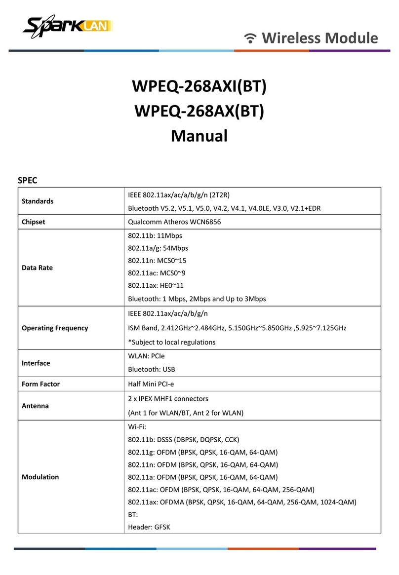
MEIG SLM 320 Guide

MeiG_SLM320_Hardware Design Manual
3KO-923.GXJ]GXK
*KYOMT3GT[GR
Controlled Version Number: V1.2
Release date:2021-06-18

MeiG_SLM320_Hardware Design Manual
MeiG Smart Technology Co., Ltd
1/89
Important Notice
Copyright Notice
All rights reserved. MeiG Smart Technology Co., Ltd
This manual and all its contents are owned by MeiG Smart Technology Co., Ltd and
protected by Chinese laws and relevant copyright laws in applicable international
conventions. Without the written authorization of MeiG Smart Technology Co., Ltd, no one
may copy, disseminate, distribute, modify or use part or all of this manual in any form, and
the offenders will be held responsible according to law.
Statement of No Guarantee
MeiG Smart Technology Co., Ltd makes no representations or guarantees, either express
or implied, for any contents in this document, and assumes no responsibility for the
merchantability and fitness for a particular purpose or any indirect, extraordinary or
consequential losses.
Confidentiality Claim
The information contained in this document (including any annexes) is confidential. The
recipient understands that the document obtained by him is confidential and shall not be
used for any purpose other than the stated purpose, and he shall not disclose this
document to any third party.
Disclaimer
The company assumes no responsibility for property damage or personal injury caused by
customers’ improper operation. Customers are requested to develop corresponding
products according to the technical specifications and reference designs in the manual.
Before the disclaimer, the company has the right to change the contents of this manual
according to the needs of technological development, and the version is subject to change
without further notice.

MeiG_SLM320_Hardware Design Manual
MeiG Smart Technology Co., Ltd
2/89
Revision History
Revision Date Description
V1.0 2020-04-21 First edition
V1.1 2021-04-22 Modify file format and correct description
V1.2 2021-06-18 Update SLM320-
LA frequency information and added RF
performance for B2/B4

MeiG_SLM320_Hardware Design Manual
MeiG Smart Technology Co., Ltd
3/89
Contents
Important Notice....................................................................................................................................... 1
Revision History ....................................................................................................................................... 2
Contents .................................................................................................................................................... 3
1 Introduction ....................................................................................................................................... 5
1.1 Safety instruction ...................................................................................................................... 6
2 Product Overview ............................................................................................................................. 7
2.1 General Description .................................................................................................................. 7
2.2 Key Features............................................................................................................................. 7
2.3 Functional block diagram........................................................................................................ 10
2.4 Evaluation Kit .......................................................................................................................... 11
3 Application Interface ...................................................................................................................... 12
3.1 General Description ................................................................................................................ 12
3.2 Pin Assignment ....................................................................................................................... 13
3.3 PIN Description ....................................................................................................................... 14
3.4 Power source .......................................................................................................................... 22
3.4.1 Power Supply................................................................................................................ 23
3.4.2 Reduce voltage drop..................................................................................................... 23
3.4.3 Power Supply Reference Circuit................................................................................... 24
3.4.4 VDD_EXT voltage output.............................................................................................. 24
3.5 Start up.................................................................................................................................... 25
3.5.1 PWRKEY Pin boot ........................................................................................................ 25
3.5.2 Power off ....................................................................................................................... 26
3.6 Reset Function........................................................................................................................ 26
3.6.1 Hardware Reset ............................................................................................................ 26
3.6.2 AT command Reset ...................................................................................................... 27
3.7 USIM/SIM Interface................................................................................................................. 28
3.8 USB port.................................................................................................................................. 30
3.8.1 USB Pin Description ..................................................................................................... 30
3.8.2 USB Reference Circuit.................................................................................................. 30
3.9 Serial Port ............................................................................................................................... 31
3.10 Status indication ..................................................................................................................... 33
3.11 Low Power Mode .................................................................................................................... 35
3.11.1 Flight mode ................................................................................................................. 35
3.11.2 Sleep mode................................................................................................................. 35
3.11.3 Ultra low power mode ................................................................................................. 36
3.12 ADC Function ......................................................................................................................... 36
3.13 USB_BOOT Port..................................................................................................................... 37
4 GNSS Receiver................................................................................................................................ 38
4.1 General Description ................................................................................................................ 38
4.2 GNSS Performance ................................................................................................................ 38
4.3 Layout Guidelines ................................................................................................................... 38
4.4 Antenna connection ................................................................................................................ 38
5 Antenna interface............................................................................................................................ 39
5.1 Introduction to Antenna Interface ........................................................................................... 39

MeiG_SLM320_Hardware Design Manual
MeiG Smart Technology Co., Ltd
4/89
5.2 Radio frequency reference circuit........................................................................................... 39
5.3 Installation of antenna............................................................................................................. 40
5.3.1 Antenna requirements................................................................................................... 40
5.3.2 RF output power ........................................................................................................... 41
5.3.3 RF reception sensitivity................................................................................................. 42
5.3.4 Working frequency ........................................................................................................ 43
5.3.5 OTA Antenna requirements ....................................................................................... 45
6 Electrical characteristics ............................................................................................................... 46
6.1 Absolute Maximum Ratings .................................................................................................... 46
6.2 Ambient Temperature Range ................................................................................................. 46
6.3 Electrical Characteristics of Interface Working State ............................................................. 46
6.4 Module Power Consumption Range....................................................................................... 47
6.5 Environmental reliability requirements.................................................................................... 78
6.6 ESD character......................................................................................................................... 78
7 Mechanical characteristics............................................................................................................ 80
7.1 Module Mechanical Dimensions............................................................................................. 80
7.2 Recommended Footprint ........................................................................................................ 81
7.3 Top View of Module ................................................................................................................ 82
7.4 Bottom View of Module........................................................................................................... 82
8 Storage and production ................................................................................................................. 83
8.1 Storage.................................................................................................................................... 83
8.2 Reflow Profile.......................................................................................................................... 83
8.3 Packaging ............................................................................................................................... 84
9 Appendix A refers to documentation and term abbreviations .................................................. 85
9.1 Reference File......................................................................................................................... 85
9.2 Symbol Key............................................................................................................................. 85
10 Appendix B GPRS Coding Scheme .............................................................................................. 89

MeiG_SLM320_Hardware Design Manual
MeiG Smart Technology Co., Ltd
5/89
1 Introduction
This document describes SLM320 module air interface and hardware interface that connected to the
clients’ applications.
This document can help customers quickly understand SLM320 module interface specification, electrical
characteristics, mechanical specifications and related product information. With the help of this
document, combined with our application manual and user instructions, customers can quickly apply
SLM320 module to wireless IoT applications.
SLM320 Wireless module is a wide band wireless terminal product applicable to
TDD-LTE/FDD-LTE/GSM, a variety of network standards.
SLM320 Supports access rate:
TDD-LTE:8Mbps/2Mbps;
FDD-LTE:10Mbps/5Mbps;
GPRS: 85.6kbps/85.6kbps;
SLM320 not only provides wireless data access, but also provides voice mesdrope and other functions.
SLM320 can be widely used in the field of M2M, such as OBD, CPE, router, data card, DTU, security and
industrial PDA, etc.

MeiG_SLM320_Hardware Design Manual
MeiG Smart Technology Co., Ltd
6/89
1.1 Safety instruction
Following below safety principles, user could ensure personal safety and protect products and work
environment from potential damage.
Driving safety first! Do not use a hand-held mobile terminal while driving, unless
it has a hands-free function. Stop before making a call!
Before boarding, please turn off the wireless function of the mobile terminal. It is
prohibited to turn on the wireless function of the mobile terminal on the airplane
to prevent interference with the airplane communication system. Ignoring this
prompt may lead to flight safety or even violate the law.
In a hospital or health care setting, be aware that there are mobile terminal
devices that may need to be turned off because limited RF interference will
cause medical devices to malfunction.
The mobile terminal device will not be able to connect effectively under all
circumstances. If the mobile device has no phone charge or the SIM is invalid,
please remember to make an emergency call when you encounter the above
situations in an emergency, and ensure that your device is turned on and in an
area with sufficient signal strength.
Your mobile terminal device will receive and transmit rf signals when it is turned
on. When it is close to TV, radio, computer or other electronic devices, RF
interference will be generated.
Keep mobile devices away from flammable gases. When you are near a gas
station, oil depot, chemical plant or explosion site, turn off mobile terminals.
Operating electronic devices in any potentially explosive site is a safety hazard.

MeiG_SLM320_Hardware Design Manual
MeiG Smart Technology Co., Ltd
7/89
2 Product Overview
2.1 General Description
SLM320 is a wireless communication module that supports TDD-LTE/FDD-LTE/GSM, supports
TDD-LTE FDD-LTE GPRS network data connection, and can provide digital voice (PCM) and analog
voice, SMS and other functions such as Wi-Fi Scan/BT, GNSS*(GPS/GLONASS/BD).
Table 1 SLM320 modules frequency band
4UZK
* GNSS is optional with a specified PN of the SLM320 module
SLM320 adopts highly integrated design scheme of the RF and baseband integrated on a single PCB,
The baseband signal processing and audio signal processing functions adopt a single-sided layout, and
the module structure size is: 32.0×29.0×2.4mm. SLM320 can be widely used in field of M2M, for
example, OBD, CPE, routers, DTU, security and industrial-grade PDA etc.
2.2 Key Features
The following table describes the detailed features of SLM320 module.
Table 2 Key features of SLM320 module
Features Details
Power supply
VBAT Supply voltage range:3.4V~4.5V
Typical supply voltage
:
3.8V
Transmitted power
Class 4 (33dBm±2dB) for GSM900 PCL5
Class 1 (30dBm±2dB) for DCS1800 PCL0
Class E2 (27dBm±3dB) for GPRS900 PCL8
Class E2 (26dBm±3dB) for GPRS1800 PCL2
Class 3 (23dBm±2.7dB) for FDD-LTE bands
Class 3 (23dBm±2.7dB) for TDD-LTE bands
Internet SLM320-E SLM320-C SLM320-LA
TDD-LTE B38/40/41 B34/B38/39/40/41 B40
FDD-LTE B1/B3/B5/B7/B8/B20 B1/B3/B5/B8 B1/B2/B3/B4/B5/B7/B8
/B20/B28
GSM 850/900/1800/1900 850/900/1800 850/900/1800/1900

MeiG_SLM320_Hardware Design Manual
MeiG Smart Technology Co., Ltd
8/89
LTE Characteristic
The maximum supportCAT1 Bis
Support 1.4 ~ 20 MHZ radio frequency bandwidth
FDD:The maximum UL rate is 5Mbps, and the maximum
DL rate is 10Mbps
TDD:He maximum UL rate is 2Mbps, and the maximum
DL rate is 8Mbps
GSM character
CSD transmission rate: 9.6 KBPS, 14.4 KBPS
Support GPRS multi - slot class 12 (the default is 12)
Coding formats: / CS-1/CS -2/CS --3 and CS - 4
Maximum 4 RX slots per frame
Network protocol features Embedded TCP/IP and UDP/IP protocol stack
Short Message service(SMS)
Text and PDU mode
point-to-point MO and MT
Short Message storage: stored in the SIM card by default
Cell broadcast
GNSS character
Cold start time<40S
Hot start time<5S
Tracking sensitivity-160dBm
Acquisition sensitivity-147dBm
Position accuracy<3m
GNSS Data type
:
NMEA-0183
USIM Port Support USIM/SIM:1.8Vand3V
Audio Features
Support 1 channel digital audio interface:PCM port
Support analog MIC signal input interface all the way
Support one loudspeaker signal output interface
(
0.8W@4.2V /D
,
0.6[email protected]V/AB
)
PCM Interface For audio use, external CODEC chip is required
USB Interface
Support USB2.0
To the AT command, data transmission, software
debugging and software upgrades
USB drive:Support Windows7,Windows 8/8.1,
Windows10
Serial Interface
The serial port:
To AT commands and data transmission
Baud rate is default 115200bps
Support RTS and CTS hardware flow control
DBG Port:
To develop debug, the log output
Baud rate is default115200bps
SD Interface Conforms to SD3.0 protocol
AT Commands
Comply with 3GPP TS 27.007, 27.005, and MeiG
enhanced AT command
Network Indicator
NET_STATUS,NET_MOD these two pins indicate the
state of the network

MeiG_SLM320_Hardware Design Manual
MeiG Smart Technology Co., Ltd
9/89
Antenna Interface Main antenna interface(ANT_MAIN)
Physical Property
Size:32.0×29.0×2.4mm
Weight
:
7 gram
Te Temperature Range
Normal operating temperature:-30℃~+75℃
Storage temperature
:
-40
℃~
+85
℃
Software Upgrading USB port/FOTA
RoHS All devices comply fully with EU RoHS standards
Environment Humidity 5%~95%
ESD
GND:+ 8 KV air discharge, the contact discharge plus or
minus 4 KV
Antenna interface: air discharge ±8KV, contact discharge
±4KV
Package 144 Pin LGA+LCC port
LCC Functional Interface
Power interface
USB2.0 High-Speed port
UART interface
USIM/SIM port(support 3V、1.8V)
PCM interface
MIC input interface
Speaker output interface
Hardware reset interface
Indicator interface
Keyboard interface
Sleep control interface
Flight mode control interface
ADC interface
I2C interface
SPI interface
SD interface
USB_BOOT port

MeiG_SLM320_Hardware Design Manual
MeiG Smart Technology Co., Ltd
10/89
2.3 Functional block diagram
Following is the functional block diagram of SLM320, illustrating its main functions.
PMU
BBU
Internal memory
The radio frequency part
peripheral interface
Figure 1 Functional block diagram

MeiG_SLM320_Hardware Design Manual
MeiG Smart Technology Co., Ltd
11/89
2.4 Evaluation Kit
To facilitate testing and use of the SLM320 module, MeiG provides an evaluation Kit to customer.
Evaluation Kit includes USB cables, antennas, and other peripherals.
Please refer to the specific use method of evaluation board MeiG_SLM320_Mini PCIe_EVB_UGD

MeiG_SLM320_Hardware Design Manual
MeiG Smart Technology Co., Ltd
12/89
3 Application Interface
3.1 General Description
SLM320 adopts LCC+LGA interface, total 144 pins, including 80 LCC pins and 64 LGA pins, providing
the following functional interfaces:
Power port
USB2.0 High-Speed port
UART port
USIM/SIM port(support 3V、1.8V)
PCM port
MIC input interface
The speaker output interface
Hardware reset interface
Pilot light interface
Keyboard interface
Sleep control interface
Flight mode control interface
ADC port
I2C port
SPI port
SD port
USB_BOOT port

MeiG_SLM320_Hardware Design Manual
MeiG Smart Technology Co., Ltd
13/89
3.2 Pin Assignment
The following figure shows the pin assignment of SLM320 module.
Figure 2 Pin Assignment
Note:
The pin name in the pin diagram is the actual wiring name inside the module.

MeiG_SLM320_Hardware Design Manual
MeiG Smart Technology Co., Ltd
14/89
3.3 PIN Description
The following table shows the definition of each pin in the SLM320 module.
Table 3 IO Parameter Definitions
Type Description
IO I/O two-way signal.
DI Digital input signal.
DO Digital output signal.
OD Open drain output signal.
AI Analog signal input
BOT Two-way signal with leaky output.
PI power input
PO power output
Table 4 Pin Description
Pin
number
Pin name I/O Electrical level Description Remark
1 WAKEUP_IN I/O VILnom=0V
VIHnom=1.8V
External device wake up
module
If not, please suspend
this pin
GPIO29
2 AP_READY I/O VILnom=0V
VIHnom=1.8V
The module checks
whether the host is
sleeping
If not, please suspend
this pin
GPIO30
3 SLEEP_IND I/O VOLnom=0V
VOHnom=1.8V
Systematic sleep
indicator
If not, please suspend
this pin
GPIO8
4 W_DISABLE# I/O VILnom=0V
VIHnom=1.8V
Modular flight mode
controlIf not, please
suspend this pin
GPIO31

MeiG_SLM320_Hardware Design Manual
MeiG Smart Technology Co., Ltd
15/89
5 NET_MODE I/O VOLnom=0V
VOHnom=1.8V
Module network mode
indication signal
If not, please suspend
this pin
GPIO13
6 NET_STATUS I/O VOLnom=0V
VOHnom=1.8V
Module network status
indicator
If not, please suspend
this pin
GPIO19
7 VDD_EXT PO 1.8V
Module digital level, 1.8V
output, 50mA load
capacity
If not, please suspend
this pin
8 GND G GND
9 GND G GND
10 USIM_GND G GND
11 DBG_RXD I VILnom=0V
VIHnom=1.8V
Debug serial port
receiving
If not, please suspend
this pin
12 DBG_TXD O VOLnom=0V
VOHnom=1.8V
Debug serial port
sending
If not, please suspend
this pin
13 USIM_PRESEN
CE I VILnom=0V
VIHnom=1.8V
USIM card hot swap
detection
If not, please suspend
this pin,
Software shutdown
detection function
14 USIM_VDD PO 1.8V/3.0V USIM power supply
15 USIM_DATA I/O 1.8V/3.0V USIM data signal line
16 USIM_CLK O 1.8V/3.0V USIM clock signal line
17 USIM_RST O 1.8V/3.0V USIM reset signal line
18 GPIO18 IO VILnom=0V
VIHnom=1.8V
If not, please suspend
this pin
The module is
internally
connected
with UART2_
RTS, default
NC

MeiG_SLM320_Hardware Design Manual
MeiG Smart Technology Co., Ltd
16/89
19 GND G GND
20 RESET_N I VILnom=0V
VIHnom=1.8V
Module reset signal, low
level valid
21 PWRKEY I VILnom=0V
VIHnom=1.8V
Module power on / off
signal
Low level active
22 GND G GND
23 SD1_DETECT I VILnom=0V
VIHnom=1.8V
SD card hot swap
detection signal
If not, please suspend
this pin
24 PCM_IN(I2S_DI) I VILnom=0V
VIHnom=1.8V
PCM data input
If not, please suspend
this pin
25 PCM_OUT(I2S_
DO) O VOLnom=0V
VOHnom=1.8V
PCM data output
If not, please suspend
this pin
26 PCM_SYNC(I2S
_SYNC) I/O 0V/1.8V
PCM data
synchronization signal
If not, please suspend
this pin
27 PCM_CLK(I2S_
CLK) I/O 0V/1.8V
PCM clock signal
If not, please suspend
this pin
28 SDC2_DATA_3 I/O 1.8V/3.0V
SDC2_DATA_3
If not, please suspend
this pin
29 SDC2_DATA_2 I/O 1.8V/3.0V
SDC2_DATA_2
If not, please suspend
this pin
30 SDC2_DATA_1 I/O 1.8V/3.0V
SDC2_DATA_1
If not, please suspend
this pin
31 SDC2_DATA_0 I/O 1.8V/3.0V
SDC2_DATA_0
If not, please suspend
this pin
32 SDC2_CLK O 1.8V/3.0V
SDC2_CLK
If not, please suspend
this pin
33 SDC2_CMD O 1.8V/3.0V
SDC2_CMD
If not, please suspend
this pin
34 VDD_SDIO PO 1.8V/3.0V
SD card pull-up power
supply, power supply
capacity 150mA

MeiG_SLM320_Hardware Design Manual
MeiG Smart Technology Co., Ltd
17/89
35 WIFI_ANT(BT_A
NT) I
WiFi / BT antenna
If not, please suspend
this pin
The module is
internally
connected
with BT_ ANT
36 GND G GND
37 SPI_CS_N O VOLnom=0V
VOHnom=1.8V
SPI chip selection signal
If not, please suspend
this pin
38 SPI_MOSI O VOLnom=0V
VOHnom=1.8V
SPI_MOSI
If not, please suspend
this pin
39 SPI_MISO I VILnom=0V
VIHnom=1.8V
SPI_MISO
If not, please suspend
this pin
40 SPI_CLK O VOLnom=0V
VOHnom=1.8V
SPI_CLK
If not, please suspend
this pin
41 I2C_SCL OD VOLnom=0V
VOHnom=1.8V
I2C interface clock signal
If not, please suspend
this pin
42 I2C_SDA BOT 0V/1.8V
I2C interface data signal
If not, please suspend
this pin
43 ADC2* AI
ADC interface 2
When in use, 1K in
series,
If not, please suspend
this pin
44 ADC1 AI
ADC interface 1
When in use, 1K in
series,
If not, please suspend
this pin
45 ADC0 AI
ADC interface 0
When in use, 1K in
series,
If not, please suspend
this pin
46 GND G GND
47 ANT_GNSS
GPS antenna
If not, please suspend
this pin
48 GND G GND
49 ANT_MAIN I/O Main collector antenna

MeiG_SLM320_Hardware Design Manual
MeiG Smart Technology Co., Ltd
18/89
50 GND G GND
51 GND G GND
52 GND G GND
53 GND G GND
54 GND G GND
55 RESERVED RESERVED
56 GND G GND
57 VBAT_RF PI
Vmax=4.5V
Vmin=3.2V
Vnorm=3.6V
RF power input Connected to
Vbat
58 VBAT_RF PI
Vmax=4.5V
Vmin=3.2V
Vnorm=3.6V
RF power input Connected to
Vbat
59 VBAT_BB PI
Vmax=4.5V
Vmin=3.2V
Vnorm=3.6V
Baseband power input Connected to
Vbat
60 VBAT_BB PI
Vmax=4.5V
Vmin=3.2V
Vnorm=3.6V
Baseband power input Connected to
Vbat
61 STATUS O VOLnom=0V
VOHnom=1.8V
Reserved status
indication interface
If not, please suspend
this pin
62 RI* O VOLnom=0V
VOHnom=1.8V
Module output ringing
prompt
If not, please suspend
this pin
GPIO22
63 UART2_TXD O VOLnom=0V
VOHnom=1.8V
Module sends data
If not, please suspend
this pin
UART2_TXD
64 CTS* O VOLnom=0V
VOHnom=1.8V
Module clear send UART1_CTS
65 RTS* O VOLnom=0V
VOHnom=1.8V
Module request sending UART1_RTS
66 UART_2_RXD O VOLnom=0V
VOHnom=1.8V
The module receives
data
UART_2_RX
D
67 MAIN_TXD O VOLnom=0V
VOHnom=1.8V
Module sends data
If not, please suspend
this pin
UART1_ TXD,
for at
command
68 MAIN_RXD I VILnom=0V
VIHnom=1.8V
The module receives
data
UART1_
RXD, for at

MeiG_SLM320_Hardware Design Manual
MeiG Smart Technology Co., Ltd
19/89
If not, please suspend
this pin
command
69 USB_DP I/O USB signal DP
70 USB_DM I/O USB signal DM
71 USB_VBUS AI Vnorm=5.0V USB insertion detection
signal
72 GND G GND
73 KEYOUT2 I
Keyboard matrix input
signal
If not, please suspend
this pin
74 KEYOUT3 I
Keyboard matrix input
signal
If not, please suspend
this pin
75 SPK_P O
SPK_P
If not, please suspend
this pin
76 RESERVED
77 SPK_N O
SPK_N
If not, please suspend
this pin
78 KEYIN1 I VILnom=0V
VIHnom=1.8V
Keyboard matrix input
signal
If not, please suspend
this pin
79 KEYIN2 I VILnom=0V
VIHnom=1.8V
Keyboard matrix input
signal
If not, please suspend
this pin
80 KEYIN3 I VILnom=0V
VIHnom=1.8V
Keyboard matrix input
signal
If not, please suspend
this pin
81 KEYIN4 I VILnom=0V
VIHnom=1.8V
Keyboard matrix input
signal
If not, please suspend
this pin
82 KEYIN5 I VILnom=0V
VIHnom=1.8V
Keyboard matrix input
signal
If not, please suspend
this pin
83 KEYOUT0 O VOLnom=0V
VOHnom=1.8V
Keyboard matrix input
signal
Table of contents
Other MEIG Wireless Module manuals


