MEIG SLM750 Series User manual
MeiGProductManualofSLM750Module
SLM750ModuleHardwareDesignPage 1, total 84 pages
MeiG Product
Manual of SLM750
VersionNumber:V1.1
Company:MeiGSmartTechnologyCo.,Ltd
ReleasedDate:2018/8/13

MeiGProductManualofSLM750Module
SLM750ModuleHardwareDesignPage 2, total 84 pages
IMPORTANTNOTICE
COPYRIGHTNOTICE
Copyright©MeiGSmartTechnologyCo.,Ltd.Allrightsreserved.
AllcontentsofthismanualareexclusivelyownedbyMeiGSmartTechnologyCo.,Ltd(MeiGSmartforshort),
whichisundertheprotectionofChineselawsandcopyrightlawsininternationalconventions.Anyoneshall
notcopy,spread,distribute,modifyoruseinotherwayswithitscontentswithoutthewritten
authorizationofMeiGSmart.Thosewhoviolatedwillbeinvestigatedbycorrespondinglegalliabilityin
accordancewiththelaw.
NOGUARANTEE
MeiGSmartmakesnorepresentationorwarranty,eitherexpressorimplied,foranycontentinthis
document,andwillnotbeliableforanyspecificmerchantabilityandapplicableoranyindirect,particular
andcollateraldamage.
CONFIDENTIALITY
Allinformationcontainedhere(includinganyattachments)isconfidential.Therecipientacknowledgesthe
confidentialityofthisdocument,andexceptforthespecificpurpose,thisdocumentshallnotbedisclosed
toanythirdparty.
DISCLAIMER
MeiGSmartwillnottakeanyresponsibilityforanypropertyandhealthdamagecausedbytheabnormal
operationofcustomers.Pleasedeveloptheproductaccordingtothetechnicalspecificationanddesigning
referenceguidewhichdefinedintheproductmanual.MeiGSmarthavetherighttomodifythedocument
accordingtotechnicalrequirementwithnoannouncementtothecustomer.
MeiGProductManualofSLM750Module
SLM750ModuleHardwareDesignPage 3, total 84 pages
Revising History
Table 1: Revising records
REVISIONDATEDESCRIPTION
V1.02018‐04‐01Initial
V1.12018‐12‐14Modifypowerconsumption,RF,packaging

MeiGProductManualofSLM750Module
SLM750ModuleHardwareDesignPage 4, total 84 pages
Contents
1 Introduction ............................................................................................................................................................ 8
1.1 Safety Information....................................................................................................................................... 9
1.1 Safety Information....................................................................................................................................... 9
1.2 Purpose ...................................................................................................................................................... 10
1.3 Content list................................................................................................................................................. 10
2 Product Overview..................................................................................................................................................11
2.1 Basic Description........................................................................................................................................11
2.2 Main performance.......................................................................................................................................11
2.3 Functional diagram .................................................................................................................................... 14
2.4 Evaluation Board ....................................................................................................................................... 15
3 Application Interface ............................................................................................................................................ 16
3.1 General Description ................................................................................................................................... 16
3.2 LCC Card Interface Definition .................................................................................................................. 17
3.3 Pin Description .......................................................................................................................................... 17
3.4 Operating Mode......................................................................................................................................... 28
3.5 Power Saving............................................................................................................................................. 30
3.5.1 Sleep Mode ..................................................................................................................................... 30
3.5.1.1 USB Application (with USB remote waking-up function) .................................................. 30
3.5.1.2 USB Application (without USB Suspend function)............................................................. 31
3.5.1.3 Hardware I/O control sleep mode........................................................................................ 31
3.5.2 Flight Mode .................................................................................................................................... 32
3.5.2.1 Hardware I/O interface controls flight mode ....................................................................... 32
3.5.2.2 AT command controls flight mode....................................................................................... 32
3.6 Power Supply............................................................................................................................................. 32
3.6.1 Power supply pins........................................................................................................................... 32
3.6.2 Decrease voltage drop..................................................................................................................... 33
3.6.3 Reference design for power supply ................................................................................................ 34
3.6.4 VDD_EXT voltage output .............................................................................................................. 35
3.7 Turn On and Off......................................................................................................................................... 35
3.7.1 Turn on module using the PWRKEY.............................................................................................. 35
3.7.2 Turn off module using the PWRKEY pin....................................................................................... 37
3.7.2.1 PWRKEY pin shutdown ...................................................................................................... 37
3.7.2.2 AT command shutdown........................................................................................................ 38
3.8 Reset the Module ....................................................................................................................................... 38
3.8.1 Hardware reset ................................................................................................................................ 39
3.8.2 AT command reset .......................................................................................................................... 40
3.9 USIM/SIM Card Interface ......................................................................................................................... 40
3.10 USB Interface .......................................................................................................................................... 42
3.10.1 USB pin description...................................................................................................................... 43
3.10.2 USB reference circuit.................................................................................................................... 43
3.10.3 USB driver.................................................................................................................................... 44
3.11 UART Interface........................................................................................................................................ 44
3.12 PCM and I2C Interface............................................................................................................................ 46

MeiGProductManualofSLM750Module
SLM750ModuleHardwareDesignPage 5, total 84 pages
3.13 Network Status Indication ....................................................................................................................... 48
3.14 Status ....................................................................................................................................................... 49
3.15 ADC Function.......................................................................................................................................... 50
3.16 SGMII Interface....................................................................................................................................... 50
3.17 Wireless Connectivity Interfaces ............................................................................................................. 52
3.17.1 WLAN Interface ........................................................................................................................... 54
3.17.2 BT Interface .................................................................................................................................. 55
3.18 SD Card Interface .................................................................................................................................... 55
3.19 USB_BOOT Interface.............................................................................................................................. 57
4 GNSS.................................................................................................................................................................... 58
4.1 General Description ................................................................................................................................... 58
4.2 GNSS Performance.................................................................................................................................... 58
4.3 Layout Guideline ....................................................................................................................................... 59
5 Antenna Interface.................................................................................................................................................. 59
5.1 Antenna Interface....................................................................................................................................... 59
5.2 RF Reference Circuit ................................................................................................................................. 60
5.3 Antenna Installation ................................................................................................................................... 62
5.3.1 Antenna requirements ..................................................................................................................... 62
5.3.2 RF output power ............................................................................................................................. 62
5.3.3 RF receiving sensitivity .................................................................................................................. 63
5.3.4 Operating frequency ....................................................................................................................... 64
5.3.5 Antenna requirements ..................................................................................................................... 64
6 Electrical characteristics ....................................................................................................................................... 65
6.1 Limit voltage range.................................................................................................................................... 65
6.2 Temperature range ..................................................................................................................................... 66
6.3 Electrical Characteristics of Interface Operation Status ............................................................................ 66
6.4 Module Power Consumption Range.......................................................................................................... 67
6.5 Environmental Reliability Requirements................................................................................................... 72
6.6 ESD Characteristics................................................................................................................................... 73
7 Mechanical Dimensions........................................................................................................................................ 74
7.1 Mechanical Dimensions of the Module ..................................................................................................... 74
7.2 Recommended Packaging.......................................................................................................................... 76
7.3 Top View of the Module ............................................................................................................................ 77
7.4 Bottom View of the Module ...................................................................................................................... 77
8 Storage and Manufacturing................................................................................................................................... 78
8.1 Storage ....................................................................................................................................................... 78
8.2 Manufacturing and Welding ...................................................................................................................... 79
8.3 Packing ...................................................................................................................................................... 79
9 Appendix A References......................................................................................................................................... 81
9.1 Related Documents.................................................................................................................................... 81
9.2 Terms and Abbreviations ........................................................................................................................... 81
10 Appendix B GPRS Coding Scheme.................................................................................................................... 83

MeiGProductManualofSLM750Module
SLM750ModuleHardwareDesignPage 6, total 84 pages
Table
TABLE 1: REVISING RECORDS....................................................................................................................................3
TABLE 2: SUPPORTED BAND OF SLM750V..............................................................................................................11
TABLE 3: LIST OF MAIN FEATURES OF THE MODULE.................................................................................................12
TABLE 4: IO PARAMETERS DEFINITION....................................................................................................................17
TABLE 5: PIN DESCRIPTION......................................................................................................................................18
TABLE 6: OVERVIEW OF OPERATING MODES...........................................................................................................28
TABLE 7: RELATED POWER SUPPLY INTERFACES.......................................................................................................33
TABLE 8: RESET_N PIN DESCRIPTION.....................................................................................................................39
TABLE 9: USIM/SIM CARD INTERFACE DESCRIPTION..............................................................................................40
TABLE 10: USB INTERFACE DESCRIPTION................................................................................................................43
TABLE 11: MAIN UART PIN DESCRIPTION................................................................................................................45
TABLE 12: DEBUG UART PIN DESCRIPTION.............................................................................................................45
TABLE 13: UART LOGICAL LEVEL...........................................................................................................................45
TABLE 14: PIN DESCRIPTION FOR PCM INTERFACE..................................................................................................48
TABLE 15: PIN DEFINITION OF NETWORK INDICATOR..............................................................................................48
TABLE 16: WORKING STATE OF THE NETWORK INDICATOR.....................................................................................49
TABLE 17: STATUS PIN DESCRIPTION.....................................................................................................................49
TABLE 18: ADC PIN DESCRIPTION............................................................................................................................50
TABLE 19: PIN DEFINITION OF SGMII INTERFACE....................................................................................................50
TABLE 20: PIN DEFINITION OF WIRELESS CONNECTIVITY INTERFACES...................................................................52
TABLE 21: PIN DEFINITION OF THE SD CARD INTERFACE........................................................................................55
TABLE 22: PIN DEFINITION OF USB_BOOT INTERFACE..........................................................................................57
TABLE 23: GNSS PERFORMANCE.............................................................................................................................58
TABLE 24: RF ANTENNA PIN DEFINITION..................................................................................................................59
TABLE 25: ANTENNA REQUIREMENTS......................................................................................................................62
TABLE 26: RF OUTPUT POWER.................................................................................................................................63
TABLE 27: RF RECEIVING SENSITIVITY....................................................................................................................63
TABLE 28: OPERATING FREQUENCY.........................................................................................................................64
TABLE 29: ANTENNA REQUIREMENTS......................................................................................................................64
TABLE 30: DIVERSITY ANTENNA REQUIREMENTS.....................................................................................................65
TABLE 31: LIMIT VOLTAGE RANGE...........................................................................................................................65
TABLE 32: TEMPERATURE RANGE............................................................................................................................66
TABLE 33: LOGICAL LEVEL OF NORMAL DIGITAL IO SIGNAL....................................................................................66
TABLE 34: ELECTRICAL CHARACTERISTICS IN POWER SUPPLY STATUS.....................................................................67
TABLE 35: CONSUMPTION........................................................................................................................................67
TABLE 36: ENVIRONMENTAL RELIABILITY REQUIREMENTS.....................................................................................72
TABLE 37: ESD PERFORMANCE PARAMETERS (TEMPERATURE:25℃,HUMIDITY:45%)..........................................73
TABLE 38: TERMS AND ABBREVIATIONS...................................................................................................................81
TABLE 39: DESCRIPTION OF CODING SCHEMES........................................................................................................83

MeiGProductManualofSLM750Module
SLM750ModuleHardwareDesignPage 7, total 84 pages
Figure
FIGURE 1FUNCTIONAL DIAGRAM............................................................................................................................15
FIGURE 2PIN ASSIGNMENT......................................................................................................................................17
FIGURE 3SLEEP MODE APPLICATION WITH USB REMOTE WAKING-UP FUNCTION....................................................31
FIGURE 4POWER REQUIREMENTS FOR BURST TRANSMISSION.................................................................................34
FIGURE 5STAR STRUCTURE OF POWER SUPPLY........................................................................................................34
FIGURE 6DC POWER SUPPLY CIRCUIT......................................................................................................................35
FIGURE 7TURN ON THE MODULE USING DRIVING CIRCUIT......................................................................................36
FIGURE 8TURN ON THE MODULE USING KEYSTROKE...............................................................................................36
FIGURE 9TIMING OF TURNING ON MODULE.............................................................................................................37
FIGURE 10 TIMING OF TURNING OFF MODULE..........................................................................................................38
FIGURE 11 REFERENCE CIRCUIT OF RESET_N BY USING DRIVING CIRCUIT............................................................39
FIGURE 12 REFERENCE CIRCUIT OF RESET_N BY USING BUTTON..........................................................................39
FIGURE 13RESET TIMING OF RESET_N...................................................................................................................40
FIGURE 14 REFERENCE CIRCUIT FOR 8-PIN USIM/SIM CONNECTOR.......................................................................41
FIGURE 15 REFERENCE CIRCUIT FOR 6-PIN USIM/SIM CONNECTOR.......................................................................41
FIGURE 16 USB REFERENCE CIRCUIT.......................................................................................................................43
FIGURE 17 REFERENCE CIRCUIT OF LEVEL CONVERSION CHIP.................................................................................46
FIGURE 18 TIMING IN SHORT FRAME MODE..............................................................................................................47
FIGURE 19 TIMING IN LONG FRAME MODE...............................................................................................................47
FIGURE 20 REFERENCE DESIGN FOR PCM CIRCUIT..................................................................................................48
FIGURE 21 REFERENCE CIRCUIT OF STATUS...........................................................................................................50
FIGURE 22 SIMPLIFIED BLOCK DIAGRAM FOR ETHERNET APPLICATION.................................................................51
FIGURE 23 REFERENCE CIRCUIT OF SGMII INTERFACE WITH PHY AR8033 APPLICATION.....................................52
FIGURE 24 REFERENCE CIRCUIT OF WIRELESS CONNECTIVITY INTERFACES WITH SLM158...................................54
FIGURE 25 REFERENCE CIRCUIT OF SD CARD APPLICATION...................................................................................56
FIGURE 26 CIRCUIT OF USB_ROOT INTERFACE.....................................................................................................58
FIGURE 27 RF REFERENCE CIRCUIT..........................................................................................................................61
FIGURE 28 GNSS ANTENNA REFERENCE CIRCUIT....................................................................................................61
FIGURE 29 MODULE TOP AND SIDE DIMENSION (UNIT:MM).....................................................................................74
FIGURE 30 MODULE BOTTOM DIMENSIONS (UNIT:MM)...........................................................................................75
FIGURE 31 TOP VIEW OF RECOMMENDED PACKAGING (UNIT:MM)...........................................................................76
FIGURE 32 TOP VIEW OF THE MODULE......................................................................................................................77
FIGURE 33 BOTTOM VIEW OF THE MODULE..............................................................................................................77
FIGURE 34 REFLOW SOLDERING TEMPERATURE PROFILE.........................................................................................79
FIGURE 35 PALLET PACKAGING(UNIT:MM)..............................................................................................................80

MeiGProductManualofSLM750Module
SLM750ModuleHardwareDesignPage 8, total 84 pages
1 Introduction
This document defines SLM750 modules and describes its air interface and hardware interface
which are connected with your application.
The document can help you quickly understand SLM750 interface specifications, electrical and
mechanical details and other related product information. Associated with application notes and
user guide, you can apply SLM750 in wireless applications easily.
SLM750 wireless module is a broadband wireless vehicle-mounted product used for various
network standards like TD-LTE/FDD LTE/WCDMA/TD-SCDMA/EVDO/CDMA/GSM.
Supported access rate of SLM750:
TD-LTE: 130Mbps/35Mbps
FDD LTE: 150Mbps/50Mbps
WCDMA reaches DC HSPA+: 42Mbps/5.76Mbps
EVDO reaches EVDO RevA: 3.1Mbps/1.8Mbps
TD-SCDMA reaches HSPA: 4.2Mbps/2.2Mbps
CDMA1x: 153.6kbps/153.6kbps
GSM reaches EDGE: 236.8kbps/236.8kbps
SLM750 provides high-speed broadband data access. In addition, it provides voice, SMS,
address book, GPS/Beidou and other functions, which can be used in mobile broadband access,
video surveillance, security, vehicle equipment and other products.

MeiGProductManualofSLM750Module
SLM750ModuleHardwareDesignPage 9, total 84 pages
1.1 Safety Information
Observing the following safety information can keep you safe and protect the product and its
working environment from potential damage.
Full attention must be given to driving at all times in order to reduce the risk
of an accident. Using a mobile while driving (even with a handsfree kit)
causes distraction and can lead to an accident. Stop the car before you make a
call.
Switch off the mobile terminal devices before boarding an aircraft. The
operation of wireless appliances in an aircraft is forbidden, so as to prevent
interference with communication systems. Ignore the note will threaten flight
safety or even break the law.
Pay attention to restrictions on the use of mobile terminal device in hospitals
or health care facilities. RF interference can cause medical equipment to run
out of order, so it is necessary to turn off the mobile terminal devices.
Mobile terminal device cannot be guaranteed to connect in all conditions, for
example no mobile fee or with an invalid SIM card. While you are in this
condition and need emergent help, remember to use emergency call. The
mobile terminal device must be switched on and in a service area with
adequate signal strength in order to make or receive a call.
Your mobile terminal device receives and transmits radio frequency signal
when it is on. RF interference can occur if it is use to close to TV set, radio,
computer or other electronic equipment.
Please keep the mobile device away from areas with potentially explosive
atmospheres. When you are near a gas station, oil depot, chemical plant or an
explosion site, please turn off your mobile terminal. There is a potential safety
hazard to operate electronic equipment at any potential explosion hazardous
locations.

MeiGProductManualofSLM750Module
SLM750ModuleHardwareDesignPage 10, total 84 pages
1.2 Purpose
This document describes basic functions and main features of SLM750 wireless module, as
well as hardware interface and its application, features of structure and electronics, and power index,
in order to guide you to embed SLM750 in various application terminals.
1.3 Content list
The document includes:
Chapter 1 introduces safety information, purpose of the document and revised records;
Chapter 2 describes basic functions and main features of SLM750 wireless module;
Chapter 3 describes functions, features, and applications of each hardware interface of
SLM750;
Chapter 4 describes related features of GNSS;
Chapter 5 introduces related information and notes of antenna interface;
Chapter 6 describes electronic features of SLM750;
Chapter 7 describes structure features and notes of SLM750;
Chapter 8 describes storage and production notes of SLM750;
Chapter 9 Appendix A: Reference documents and abbreviations;
Chapter 10 Appendix B: GPRS encoding scheme
MeiGProductManualofSLM750Module
SLM750ModuleHardwareDesignPage 11, total 84 pages
2 Product Overview
2.1 Basic Description
SLM750 is a wireless communication module of TD-LTE/FDD LTE/TD-SCDMA/WCDMA/
EVDO/CDMA/GSM with diversity receiving function. It supports TD-LTE and FDD LTE, and
downwards compatible with DC-HSPA+ of WCDMA, TD-HSPA of TD-SCDMA, network data
connection of EVDO RevB, which provides functions of voice, analog voice, SMS, and
communication for your applications. The module has 3 sub-modes: SLM750VC, SLM750VE,
SLM750VA. The following table shows the supported bands of the module.
Table 2: Supported band of SLM750
Network SLM750VC SLM750VE SLM750VA
TD-LTE B38/B39/B40/B41 B40 B41
FDD LTE B1/B3/B5/B8 B1/B3/B5/B7/B8/B20 B2/B4/B5/B12/B13/B17/B25/B26
WCDMA B1/B8 B1/B5/B8 B2/B4/B5
TD-SCDMA B34/B39 Not supported Not supported
EVDO Not supported Not supported Not supported
CDMA BC0 Not supported BC0/BC1
GSM 900/1800 900/1800 850/1800
GPS L1 Supported Supported Supported
Using advanced highly integrated design, SLM750 integrates RF and baseband on a piece of
PCB which has functions of wireless reception and transmission, baseband signal processing and
audio signal processing. It uses double side layout and the size is: 32.0×29.0×2.4mm. The module
can meet most M2M application requirements like mobile broadband access, video surveillance,
handheld terminals, on-board equipment, ultra-books and other products. In addition, SLM750 is
compatible with Qualcomm MDM9628 main chip, which can be used in vehicle-mounted application.
2.2 Main performance
The following table describes the performance of the SLM750 in detail.
MeiGProductManualofSLM750Module
SLM750ModuleHardwareDesignPage 12, total 84 pages
Table 3: List of main features of the module
Parameter Description
Power supply VBAT supply voltage range: 3.3V~4.2V
Typical supply voltage: 3.8V
Transmit power Class 4 (33dBm±2dB) for GSM850
Class 4 (33dBm±2dB) for GSM900
Class 1 (30dBm±2dB) for DCS1800
Class 1 (30dBm±2dB) for PCS1900
Class E2 (27dBm±3dB) for GSM850 8-PSK
Class E2 (27dBm±3dB) for GSM900 8-PSK
Class E2 (26dBm±3dB) for DCS1800 8-PSK
Class E2 (26dBm±3dB) for PCS1900 8-PSK
Class 3 (24dBm±1dB) for CDMA BC0
Class 3 (23dBm±2dB) for WCDMA bands
Class 3 (23dBm±2dB) for TD-SCDMA bands
Class 3 (23dBm±2dB) for LTE FDD bands
Class 3 (23dBm±2dB) for TD-LTE bands
LTE features Maximum support non-CA CAT4
Support 1.4 ~ 20MHz RF bandwidth
Downlink supports multi-user MIMO
FDD: maximum uplink rate 50Mbps,maximum
downlink rate 150Mbps
TDD: maximum uplink rate 35Mbps,maximum
downlink rate 130Mbps
WCDMA features Support 3GPP R8 DC-HSPA+
Support 16-QAM,64-QAM and QPSK modulation
3GPP R6 CAT6 HSUPA: maximum uplink rate
5.76Mbps
3GPP R8 CAT24 DC-HSPA+: maximum uplink rate
42Mbps
TD-SCDMA features Support CCSA Release3
Maximum uplink rate 2.2Mbps,maximum downlink rate
4.2Mbps
CDMA features Support CDMA 1X Advanced,1XEV-DOr0/-DOrA
maximum uplink rate 1.8Mbps,maximum downlink rate
3.1Mbps
GSM features R99:
CSD transmission rate: 9.6kbps,14.4kbps
GPRS:
Support GPRS multi-slot class 12(default 12)
Coding format: CS-1/CS-2/CS-3 and CS-4
Maximum 4 RX slots per frame
EDGE:
MeiGProductManualofSLM750Module
SLM750ModuleHardwareDesignPage 13, total 84 pages
Support EDGE multi-slot class 12(default 12)
Support GMSK and 8-PSK
Downlink coding format: CS 1-4 and MCS 1-9
Uplink coding format: CS 1-4 and MCS 1-9
Network protocol features Support
TCP/UDP/PPP/FTP/HTTP/SMTP/MMS/NTP/PING
/QMI protocol
Support PAP(Password Authentication Protocol)and
CHAP(Challenge Handshake Authentication Protocol)
Short message service Text and PDU mode
Point to point MO and MT
Short message cell broadcast
Short message storage: default stored in module
Multimedia message service AP terminal is required to realize MMS protocol
USIM card interface Support USIM/SIM card: 1.8V and 3V
Audio features Support 1 channel digital audio interface: PCM interface
GSM: HR/FR/EFR/AMR/AMR-WB
WCDMA: AMR/AMR-WB
LTE: AMR/AMR-WB
Support echo cancellation and noise suppression
PCM interface For audio use, need to connect the codec chip
Support 8 bit A-law, u-law and 16 bit Linear coding
format
Support long frame mode and short frame mode
Support master mode and slave mode, but in the long
frame it can only be used as the master mode
USB interface Compatible USB2.0 features (only support slave
mode),maximum data transfer rate reaches 480Mbps
Used for AT command, data transmission, GNSS NMEA
output, software debugging and software upgrading
USB drive: support Windows7, Windows8/8.1,
Windows10, Linux 2.6 or higher version, Android
2.3/4.0/4.2/4.4/5.0/5.1/6.0/7.0
Serial port Main serial port:
Used for AT commands and data transfer
Maximum baud rate is 3000000bps,default 115200bps
Support RTS and CTS hardware flow control
Debug serial port:
Used for Linux control, log output
Baud rate is 115200bps
RX-diversity Support LTE/WCDMA/CDMA RX-diversity
AT command Confirm to 3GPP TS 27.007, 27.005 and added new
MeiG AT commands
Network indication The two pins NET_STATUS,NET_MODE indicate the
network status
MeiGProductManualofSLM750Module
SLM750ModuleHardwareDesignPage 14, total 84 pages
Antenna interface Include main antenna(ANT_MAIN),RX-D diversity
antenna(ANT_DIV) and GNSS antenna(ANT_GNSS)
Physical features
Size: 32.0×29.0×2.4mm
Weight: <5 g
Temperature range Normal operating temperature: -30℃~+75℃
Limited operating temperature: -40℃~+85℃
Storage temperature: -45℃~+90℃
Software upgrade USB interface
RoHS All hardware components fully comply with the EU
RoHS standard
Ambient humidity 5%~95%
ESD VBAT,GND: Air discharge ±10KV,Contact discharge
±5KV
Antenna interface: Air discharge ±8KV,Contact
discharge ±4KV
Other interface: Air discharge ±1KV,Contact discharge
±0.5KV
Interface 144Pin LCC interface
LCC function interface Power interface
USB2.0 High-Speed interface
UART interface
USIM/SIM card interface (support 3V、1.8V)
PCM interface
Hardware reset interface
Indicator light interface
Sleep control interface
Flight mode control interface
ADC interface
I2C interface
SGMII interface
SD card interface
WLAN interface
BT_UART interface
USB_BOOT interface
2.3 Functional diagram
The following figure shows a block diagram of SLM750 and illustrates the major functional
parts.
Power management
Baseband chip
DDR+NAND storage
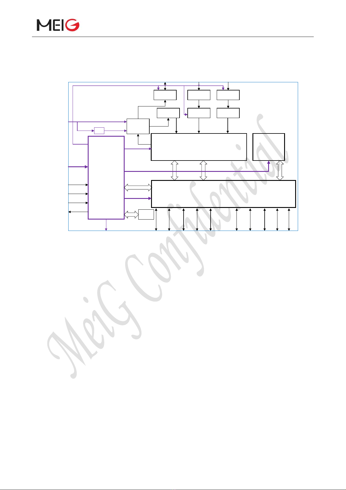
MeiGProductManualofSLM750Module
SLM750ModuleHardwareDesignPage 15, total 84 pages
Radio frequency
Peripheral interface
30
Switch SAW Switch
ANT_MAIN ANT_GNSS ANT_DIV
Duplex
PA
LNA SAW
DRx
PRx
Tx
VBAT_RF
APT
VBAT_BB PMIC
PWRKEY
RESET_N
ADCs
STATUS
Control
19.2M
XO
VDD_EXT USB USIM PCM I2C UARTs WLAN BT GPIOs SD SGMII
Baseband
Transceiver
NAND
DDR2
SDRAM
Control
IQ
Figure 1 Functional Diagram
2.4 Evaluation Board
In order to help you develop applications with SLM750, MeiG supplies an evaluation board,
Which contains USB data cable, antenna and other peripherals to control or test the module.
See MeiG_U_EVB User Guide for specific usage of evaluation board.

MeiGProductManualofSLM750Module
SLM750ModuleHardwareDesignPage 16, total 84 pages
3 Application Interface
3.1 General Description
SLM750 uses LCC+LGA interface with a total of 144 PIN among which there are 80 LCC
pins and 64 LGA pins, providing the following function interface:
Power interface
USIM/SIM interface
USB interface
UART interface
PCM interface
I2C interface
Hardware reset interface
Status indication interface
Sleep control interface
Flight mode control interface
ADC interface
SGMII interface
SD card interface
WLAN interface
BT_UART interface
USB_BOOT interface

MeiGProductManualofSLM750Module
SLM750ModuleHardwareDesignPage 17, total 84 pages
3.2 LCC Card Interface Definition
52 51 50 49 48 144 143 47 46 45 44 43 42 41 40 39 38 37
1 2 3 4 5 6 7 141 142 8 9 10 11 12 13 14 15 16
69
68
67
66
65
64
63
114
113
72
71
70
23
24
25
26
27
28
29
116
115
19
20
21
22
GNDPOWER WLAN&BT USBSGMII Signals ANT Reserved
GND
GND
GND
ANT_MAIN
GND
Reserved
Reserved
GND
ADC0
ADC1
Reserved
I2C_SDA
I2C_SCL
BT_CTS
BT_TXD
BT_RTS
SD_DATA2
SD_DATA3
PCM_CLK
PCM_SYNC
PCM_OUT
USB_BOOT
Reserved
USIM_CLK
USIM_DATA
GND
USIM_GND
USIM_PRESENCE
USIM_VDD
GND
DBG_RXD
DBG_TXD
Reserved
VDD_EXT
NET_STATUS
NET_MODE
W_DISABLE#
WAKEUP_OUT_N
AP_READY
WAKEUP_IN
Reserved
GND
USB_VBUS
RXD
TXD
DCD
Reserved
CTS
USB_DP
DTR
RTS
USB_DM
17 18
36
35
34
33
32
31
30
GND
ANT_DIV
VDD_SDIO
SD_CMD
SD_CLK
SD_DATA0
61
60
59
58
57
56
55
62
54 53
USIM_RST
SD_DATA1
PCM_IN
SD_INS_DET
GND
PWRKEY
RESET_N
GND
ANT_GNSS
GND
GND
RI
VBAT_BB
VBAT_BB
GND
Reserved
VBAT_RF
VBAT_RF
STATUS
85 86 87 88 89
73
90 91 92 93 94
95 96 97 98
99 100 101 102
103 10 4 105 106 107
108 10 9 11 0 111 112
74 75
76
79
82
129 130 131 132 133 134 135 136 13 7 138 13 9 14 0
77 78
80 81
83 84
117 118 119 12 0 12 1 122 123 124 125 126 127 128
BT_RXD
Reserved
WLAN_SLP_CLK
EPHY_RST_N
EPHY_INT_N
SGMII_MDATA
SGMII_MCLK
SGMII_TX_M
SGMII_TX_P
SGMII_RX_P
SGMII_RX_M
PM_ENABLE
USIM2_VDD
SDC1_DATA3
SDC1_DATA2
SDC1_DATA1
SDC1_DATA0
SDC1_CLK
SDC1_CMD
WA KE _ON_
WIRELESS
WLAN_EN
COEX_UART_RX
COEX_UART_TX
BT_EN
SD
Reserved
Reserved
Reserved
Figure 2 Pin Assignment
3.3 Pin Description
The following table shows the SLM750’s pin definition.
Table 4: IO Parameters Definition
Type Description
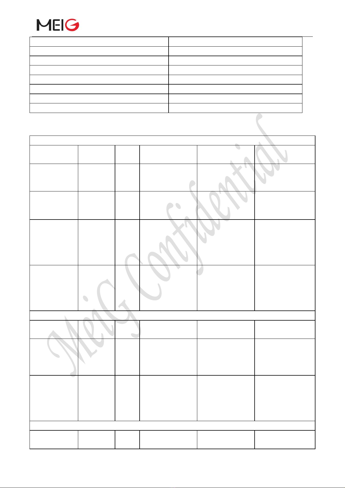
MeiGProductManualofSLM750Module
SLM750ModuleHardwareDesignPage 18, total 84 pages
IO Input output
DI Digital input
DO Digital output
PI Power input
PO Power output
AI Analog input
AO Analog output
OD Open drain
Table 5: Pin description
Power Supply
Pin name Pin
number
I/O Description DC features Note
VBAT_BB 59,60 PI Power supply for
module baseband
Vmax=4.2V
Vmin=3.3V
Vnorm=3.8V
It must be able to
provide sufficient
current up to 1A
VBAT_RF 57,58 PI Power supply for
module RF
Vmax=4.2V
Vmin=3.3V
Vnorm=3.8V
It must be able to
provide sufficient
current up to 2A
VDD_EXT
7 PO 1.8V output Vnorm=1.8V
Iomax=80mA
Power supply for
external GPIO’s
pull up circuits;
If unused, keep it
open
GND 8,9,19,22,
36,46,48,
50~54,
56,72,
85~112
- Ground - -
Turn on/off
Pin name Pin
number
I/O Description DC features Note
RESET_N 20 DI Reset the module VIHmax=2.1V
VIHmin=1.3V
VILmax=0.5V
1.8V power
domain; active low
level. If unused,
keep it open
PWRKEY 21 DI
Turn on/Standby
VIHmax=2.1V
VIHmin=1.3V
VILmax=0.5V
Diode voltage drop
inside Qualcomm
chip results in
0.8V output of the
pin
Module status indication
Pin name Pin
number
I/O Description DC features Note
MeiGProductManualofSLM750Module
SLM750ModuleHardwareDesignPage 19, total 84 pages
STATUS 61 OD Indicate the
module operating
status
Driving current
should be less
than 0.9mA
Require external
pull-up. If unused,
keep it open
NET_MODE 5 OD Indicate the
module network
registration status
VOHmin=1.35V
VOLmax=0.45V
1.8V power
domain, require
external pull-up. If
unused, keep it
open
NET_STATU
S
6 OD Indicate the
module network
running status
VOHmin=1.35V
VOLmax=0.45V
1.8V power
domain, require
external pull-up. If
unused, keep it
open
USB interface
Pin name Pin
number
I/O Description DC features Note
USB_VBUS
71 PI USB detection
Vmax=5.25V
Vmin=3.0V
Vnorm=5.0V
USB_DP 69 IO USB differential
data positive
signal
Compliant with
USB2.0 standard
specification
Require
differential
impedance of 90Ω
USB_DM 70 IO USB differential
data negative
signal
Compliant with
USB2.0 standard
specification
Require
differential
impedance of 90Ω
USIM card interface
Pin name Pin
number
I/O Description DC features Note
USIM_DATA 15 IO USIM card data
bus
1.8V USIM:
VILmax=0.6V
VIHmin=1.2V
VOLmax=0.45V
VOHmin=1.35V
3.0V USIM:
VILmax=1.0V
VIHmin=1.95V
VOLmax=0.45V
VOHmin=2.55V
-
USIM_CLK 16 DO USIM card clock
line
1.8V USIM:
VOLmax=0.45V
VOHmin=1.35V
3.0V USIM:
VOLmax=0.45V
-
MeiGProductManualofSLM750Module
SLM750ModuleHardwareDesignPage 20, total 84 pages
VOHmin=2.55V
USIM_RST 17 DO USIM card reset
line
1.8V USIM:
VOLmax=0.45V
VOHmin=1.35V
3.0V USIM:
VOLmax=0.45V
VOHmin=2.55V
-
USIM_PRESE
NCE
13 DI USIM card
detection
VILmin=-0.3V
VILmax=0.6V
VIHmin=1.2V
VIHmax=2.0V
1.8Vpower
domain, require
external pull-up to
1.8V
USIM_VDD 14 PO USIM card
supply voltage
1.8V USIM:
Vmax=1.9V
Vmin=1.7V
3.0V USIM:
Vmax=3.05V
Vmin=2.7V
Iomax=50mA
Either 1.8V or
3.0V USIM card is
identified by the
module
automatically
USIM_GND 10 USIM card
ground
Connect with
module ground
Main serial port
Pin name Pin
number
I/O Description DC features Note
RI 62 DO Ring indicator VOLmax=0.45V
VOHmin=1.35V
1.8V power
domain.
If unused, keep
it open.
DCD 63 DO Carrier detect VOLmax=0.45V
VOHmin=1.35V
1.8V power
domain.
If unused, keep
it open.
DTR 66 DI DTE ready, sleep
mode control
VILmin=-0.3V
VILmax=0.6V
VIHmin=1.2V
VIHmax=2.0V
1.8V power
domain.
If unused, keep
it open.
RXD 68 DI Receive data VILmin=-0.3V
VILmax=0.6V
VIHmin=1.2V
VIHmax=2.0V
1.8V power
domain.
If unused, keep
it open.
TXD 67 DO Transmit data VOLmax=0.45V
VOHmin=1.35V
1.8V power
domain.
If unused, keep
it open.
CTS 64 DI Clear to send VOLmax=0.45V 1.8V power
This manual suits for next models
3
Table of contents
Other MEIG Wireless Module manuals


