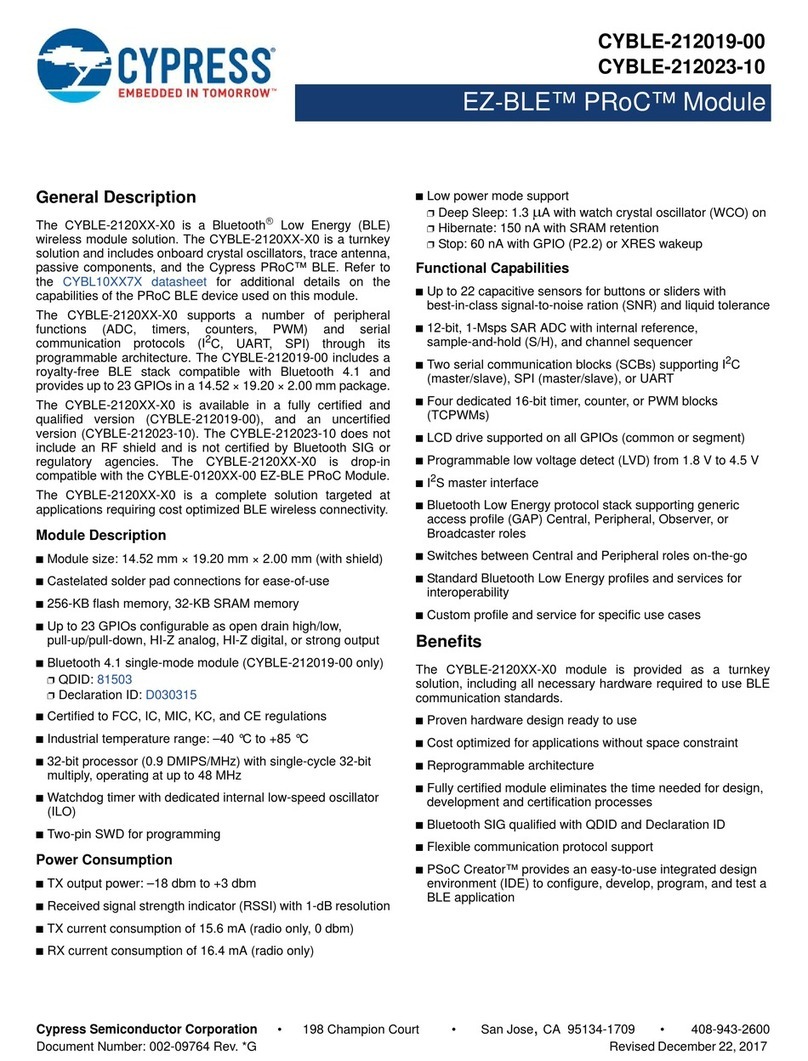
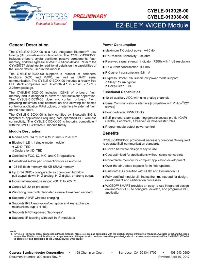
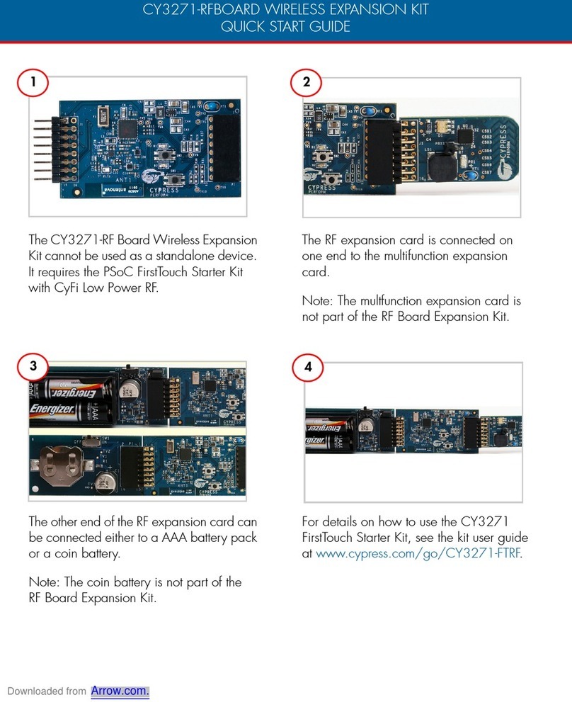
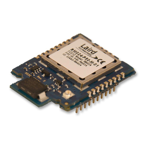
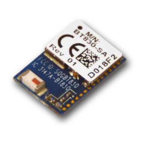
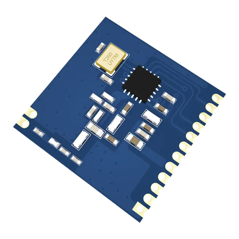
Cypress EZ-BLE PRoC XR Module User manual

PRELIMINARY
CYBLE-212006-01
CYBLE-202007-01
CYBLE-202013-11
EZ-BLE™ PRoC™ XR Module
Cypress Semiconductor Corporation • 198 Champion Court • San Jose,CA 95134-1709 • 408-943-2600
Document Number: 002-15631 Rev.*B Revised December 16, 2016
General Description
The CYBLE-2X20XX-X1 is a BluetoothLow Energy (BLE)
wireless module solution. The CYBLE-2X20XX-X1 is a turnkey
solution and includes onboard crystal oscillators, passive
components, and the Cypress PRoC™ BLE. Refer to the
CYBL1XX7X datasheet for additional details on the capabilities
of the PRoC BLE device used on this module.
The CYBLE-2X20XX-X1 supports a number of peripheral
functions (ADC, timers, counters, PWM) and serial
communication protocols (I2C, UART, SPI) through its
programmable architecture. The CYBLE-2X20XX-X1 includes a
royalty-free BLE stack compatible with Bluetooth 4.2 and
provides up to 19 GPIOs in a 15.0 × 23.0 × 2.0 mm package.
The CYBLE-2X20XX-X1 is offered in two fully certified versions
(CYBLE-212006-01 and CYBLE-202007-01), as well as an
uncertified version (CYBLE-202013-11). The CYBLE-212006-01
includes an integrated trace antenna. The CYBLE-202007-01
supports an external antenna via a u-FL connector. The
CYBLE-202013-11 supports an external antenna through a RF
solder pad output. The CYBLE-202013-11 does not include a RF
shield and is not Bluetooth SIG or regulatory certified.
Module Description
■Module size: 15.00 mm × 23.00 mm × 2.00 mm
■Extended Range:
❐Up to 400 meters bidirectional communication[1,2]
❐Up to 450 meters in beacon only mode[1]
■Bluetooth 4.2 qualified single-mode module
❐QDID: 88957
❐Declaration ID: D032786
■Footprint compatible options for integrated antenna or
antenna-less design options
■Certified to FCC, IC, MIC, KC, and CE regulations
(CYBLE-212006-01 and CYBLE-202007-01 only)
■Castelated solder pad connections for ease-of-use
■256-KB flash memory, 32-KB SRAM memory
■Up to 19 GPIOs
■Industrial temperature range: –40 °C to +85 °C
■32-bit processor (0.9 DMIPS/MHz) operating up to 48 MHz
■Watchdog timer with dedicated internal low-speed oscillator
Power Consumption
■Maximum TX output power: +7.5 dbm
■RX Receive Sensitivity: –93 dbm
■Received signal strength indicator (RSSI) with 1-dB resolution
■TX current consumption
❐BLE silicon: 15.6 mA (radio only, 0 dbm)
❐RFX2401C: 27 mA (PA/LNA only, +7.5 dBm)
■RX current consumption
❐BLE silicon: 16.4 mA (radio only, 0 dbm)
❐RFX2401C: 8.0 mA (PA/LNA only)
■Cypress CYBL1XX7X silicon low power mode support
❐Deep Sleep: 1.3 A with watch crystal oscillator (WCO) on
❐Hibernate: 150 nA with SRAM retention
❐Stop: 60 nA with XRES wakeup
Functional Capabilities
■Up to 18 capacitive sensors for buttons or sliders
■12-bit, 1-Msps SAR ADC with internal reference,
sample-and-hold (S/H), and channel sequencer
■Two serial communication blocks (SCBs) supporting I2C
(master/slave), SPI (master/slave), or UART
■Four dedicated 16-bit timer, counter, or PWM blocks
(TCPWMs)
■LCD drive supported on all GPIOs (common or segment)
■Programmable low voltage detect (LVD) from 1.8 V to 4.5 V
■I2S master interface
■BLE protocol stack supporting generic access profile (GAP)
Central, Peripheral, Observer, or Broadcaster roles
■Switches between Central and Peripheral roles on-the-go
■Standard BLE profiles and services for interoperability
■Custom profile and service for specific use cases
Benefits
CYBLE-2X20XX-X1 is provided as a turnkey solution, including
all necessary hardware required to use BLE communication
standards.
■Proven hardware design ready to use
■Cost optimized for applications without space constraint
■Reprogrammable architecture
■Fully certified module eliminates the time needed for design,
development and certification
■Bluetooth SIG qualified with QDID and Declaration ID
■Flexible communication protocol support
■PSoC Creator™ provides an easy-to-use integrated design
environment (IDE) to configure, develop, program, and test a
BLE application
Notes
1. Connection range tested module-to-module in full line-of-sight environment, free of obstacles or interference sources with output power of +7.5 dBm.
2. Specified as EZ-BLE XR module to module range. Mobile phone connection range will decrease based on the PA/LNA performance of the mobile phone used.
Document Number: 002-15631 Rev.*B Page 2 of 39
PRELIMINARY
CYBLE-212006-01
CYBLE-202007-01
CYBLE-202013-11
More Information
Cypress provides a wealth of data at www.cypress.com to help you to select the right module for your design, and to help you to
quickly and effectively integrate the module into your design.
■Overview: EZ-BLE Module Portfolio, Module Roadmap
■EZ-BLE PRoC Product Overview
■PRoC BLE Silicon Datasheet
■Application notes: Cypress offers a number of BLE application
notescoveringabroadrangeoftopics,frombasictoadvanced
level. Recommended application notes for getting started with
EZ-BLE modules are:
❐AN96841 - Getting Started with EZ-BLE Module
❐AN94020 - Getting Started with PRoC BLE
❐AN97060 - PSoC®4 BLE and PRoC™ BLE - Over-The-Air
(OTA) Device Firmware Upgrade (DFU) Guide
❐AN91162 - Creating a BLE Custom Profile
❐AN91184 - PSoC 4 BLE - Designing BLE Applications
❐AN92584 - Designing for Low Power and Estimating Battery
Life for BLE Applications
❐AN85951 - PSoC®4 CapSense®Design Guide
❐AN95089 - PSoC®4/PRoC™ BLE Crystal Oscillator Selec-
tion and Tuning Techniques
❐AN91445 - Antenna Design and RF Layout Guidelines
■Technical Reference Manual (TRM):
❐PRoC®BLE Technical Reference Manual
■Knowledge Base Articles
❐KBA216542 - Pin Mapping Differences Between the
EZ-BLE™ PRoC® Evaluation Boards (CY-
BLE-212006-EVAL/CYBLE-202007-EVAL/CY-
BLE-202013-EVAL) and the BLE Pioneer Kit
(CY8CKIT-042-BLE)
❐KBA97095 - EZ-BLE™ Module Placement
❐KBA216380 - RF Regulatory Certifications for CY-
BLE-212006-01 and CYBLE-202007-01 EZ-BLE™ PRoC®
XR Modules
❐KBA213976-FAQforBLEandRegulatoryCertificationswith
EZ-BLE modules
❐KBA210802 - Queries on BLE Qualification and Declaration
Processes
■Development Kits:
❐CYBLE-212006-EVAL, CYBLE-212006-01 Eval Board
❐CYBLE-202007-EVAL, CYBLE-202007-01 Eval Board
❐CYBLE-202013-EVAL, CYBLE-202013-11 Eval Board
❐CY8CKIT-042-BLE, Bluetooth®Low Energy Pioneer Kit
❐CY8CKIT-002, PSoC®MiniProg3 Program and Debug Kit
■Test and Debug Tools:
❐CYSmart, Bluetooth®LE Test and Debug Tool (Windows)
❐CYSmart Mobile, Bluetooth®LE Test and Debug Tool
(Android/iOS Mobile App)
Two Design Environments to Get You Started Quickly
PSoC®Creator™IntegratedDesignEnvironment(IDE)
PSoC Creator is an Integrated Design Environment (IDE) that enables concurrent hardware and firmware editing, compiling and
debugging of PSoC 3, PSoC 4, PSoC 5LP, PSoC 4 BLE, PRoC BLE and EZ-BLE module systems with no code size limitations. PSoC
peripherals are designed using schematic capture and simple graphical user interface (GUI) with over 120 pre-verified,
production-ready PSoC Components™.
PSoC Components are analog and digital “virtual chips,” represented by an icon that users can drag-and-drop into a design and
configure to suit a broad array of application requirements.
Bluetooth Low Energy Component
The Bluetooth Low Energy Component inside PSoC Creator provides a comprehensive GUI-based configuration window that lets you
quickly design BLE applications. The Component incorporates a Bluetooth Core Specification v4.1 compliant BLE protocol stack and
provides API functions to enable user applications to interface with the underlying Bluetooth Low Energy Sub-System (BLESS)
hardware via the stack.
EZ-Serial™ BLE Firmware Platform
The EZ-Serial Firmware Platform provides a simple way to access the most common hardware and communication features needed
in BLE applications. EZ-Serial implements an intuitive API protocol over the UART interface and exposes various status and control
signals through the module’s GPIOs, making it easy to add BLE functionality quickly to existing designs. Use a simple serial terminal
and evaluation kit to begin development without requiring an IDE. Refer to the EZ-Serial webpage for user manuals and instructions
for getting started as well as detailed reference materials.
EZ-BLE modules are pre-flashed with the EZ-Serial Firmware Platform. If you do not have EZ-Serial pre-loaded on your module, you
can download each EZ-BLE module’s firmware images on the EZ-Serial webpage.
Technical Support
■Frequently Asked Questions (FAQs): Learn more about our BLE ECO System.
■Forum: See if your question is already answered by fellow developers on the PSoC 4 BLE and PRoC BLE forums.
■Visit our support page and create a technical support case or contact a local sales representatives. If you are in the United States,
you can talk to our technical support team by calling our toll-free number: +1-800-541-4736. Select option 2 at the prompt.

Document Number: 002-15631 Rev.*B Page 3 of 39
PRELIMINARY
CYBLE-212006-01
CYBLE-202007-01
CYBLE-202013-11
Contents
Overview............................................................................ 4
Module Description...................................................... 4
Pad Connection Interface ................................................ 6
Recommended Host PCB Layout ................................... 7
Digital and Analog Capabilities and Connections......... 9
Power Supply Connections and Recommended External
Components.................................................................... 10
Connection Options................................................... 10
External Component Recommendation .................... 10
Critical Components List ........................................... 13
Antenna Design......................................................... 13
Qualified Antenna for CYBLE-202007-01 and CY-
BLE-202013-11 ................................................................ 13
Power Amplifier (PA) and Low Noise Amplifier (LNA) 13
Enabling Extended Range Feature........................... 14
Low Power Operation................................................ 14
Electrical Specification.................................................. 15
GPIO ......................................................................... 17
XRES......................................................................... 18
Digital Peripherals..................................................... 21
Serial Communication............................................... 23
Memory ..................................................................... 24
System Resources.................................................... 24
Environmental Specifications....................................... 30
Environmental Compliance ....................................... 30
RF Certification.......................................................... 30
Safety Certification.................................................... 30
Environmental Conditions ......................................... 30
ESD and EMI Protection ........................................... 30
Regulatory Information.................................................. 31
FCC........................................................................... 31
Industry Canada (IC) Certification............................. 32
European R&TTE Declaration of Conformity ............ 32
MIC Japan................................................................. 33
KC Korea................................................................... 33
Packaging........................................................................ 34
Ordering Information...................................................... 36
Part Numbering Convention...................................... 36
Acronyms........................................................................ 37
Document Conventions................................................. 37
Units of Measure....................................................... 37
Document History Page................................................. 38
Sales, Solutions, and Legal Information...................... 39
Worldwide Sales and Design Support....................... 39
Products.................................................................... 39
PSoC® Solutions ...................................................... 39
Cypress Developer Community................................. 39
Technical Support ..................................................... 39

Document Number: 002-15631 Rev.*B Page 4 of 39
PRELIMINARY
CYBLE-212006-01
CYBLE-202007-01
CYBLE-202013-11
Overview
Module Description
The CYBLE-2X20XX-X1 module is a complete module designed to be soldered to the applications main board.
Module Dimensions and Drawing
Cypress reserves the right to select components (including the appropriate BLE device) from various vendors to achieve the BLE
module functionality. Such selections will still guarantee that all height restrictions of the component area are maintained. Designs
should be held within the physical dimensions shown in the mechanical drawings in Figure 1 on page 5. All dimensions are in
millimeters (mm).
Table 1. Module Design Dimensions
See Figure 1 on page 5 for the mechanical reference drawing for CYBLE-2X20XX-X1.
Dimension Item Specification
Module dimensions Length (X) 15.00 ± 0.15 mm
Width (Y) 23.00 ± 0.15 mm
Antenna location dimensions Length (X) 15.00 ± 0.15 mm
Width (Y) 4.65 ± 0.15 mm
PCB thickness Height (H) 0.80 ± 0.10 mm
Shield height Height (H) 1.20 ± 0.10 mm
Maximum component height Height (H) 1.20 mm typical (shield) - CYBLE-212006-01
1.25 mm typical (connector) - CYBLE-202007-01
0.75mm typical (crystal) - CYBLE-202013-11
Total module thickness (bottom of module to highest component) Height (H) 2.00 mm typical - CYBLE-212006-01
2.05 mm typical - CYBLE-202007-01
1.55 mm typical - CYBLE-202013-11

Document Number: 002-15631 Rev.*B Page 5 of 39
PRELIMINARY
CYBLE-212006-01
CYBLE-202007-01
CYBLE-202013-11
Figure 1. Module Mechanical Drawing
Top View
Bottom View
Side View
Note
3. Nometalortracesshouldbelocatedbeneathor abovetheantennaarea.OnlybarePCBmaterialshouldbelocatedbeneaththeantennaarea.Formoreinformation
on recommended host PCB layout, see Figure 3, Figure 4, Figure 5, and Figure 6 and Table 3.

Document Number: 002-15631 Rev.*B Page 6 of 39
PRELIMINARY
CYBLE-212006-01
CYBLE-202007-01
CYBLE-202013-11
Pad Connection Interface
As shown in the bottom view of Figure1on page5, the CYBLE-2X20XX-X1 connects to the host board via solder padson the backside
of the module. Table 2 and Figure 2 detail the solder pad length, width, and pitch dimensions of the CYBLE-2X20XX-X1 module.
Figure 2. Solder Pad Dimensions (Seen from Bottom)
To maximize RF performance, the host layout should follow these recommendations:
1. The ideal placement of the Cypress BLE module is in a corner of the host board with the trace antenna located at the far corner.
This placement minimizes the additional recommended keep out area stated in item 2. Please refer to AN96841 for module
placement best practices.
2. To maximize RF performance, the area immediately around the Cypress BLE module trace antenna should contain an additional
keep out area, where no grounding or signal trace are contained. The keep out area applies to all layers of the host board. The
recommended dimensions of the host PCB keep out area are shown in Figure 3 (dimensions are in mm).
Figure 3. Recommended Host PCB Keep Out Area Around the CYBLE-2X20XX-X1 Antenna
Table 2. Solder Pad Connection Description
Name Connections Connection Type Pad Length Dimension Pad Width Dimension Pad Pitch
SP 30 Solder Pads 1.02 mm 0.71 mm 1.27 mm
Host PCB Keep Out Area Around Trace Antenna

Document Number: 002-15631 Rev.*B Page 7 of 39
PRELIMINARY
CYBLE-212006-01
CYBLE-202007-01
CYBLE-202013-11
Recommended Host PCB Layout
Figure 4, Figure 5, Figure 6, and Table 3 provide details that can be used for the recommended host PCB layout pattern for the
CYBLE-212006-01. Dimensions are in millimeters unless otherwise noted. Pad length of 1.27 mm (0.635 mm from center of the pad
on either side) shown in Figure 6 is the minimum recommended host pad length. The host PCB layout pattern can be completed using
either Figure 4, Figure 5, or Figure 6. It is not necessary to use all figures to complete the host PCB layout pattern.
Figure 4. Host Layout Pattern for CYBLE-2X20XX-X1 Figure 5. Module Pad Location from Origin
Top View (Seen on Host PCB)

Document Number: 002-15631 Rev.*B Page 8 of 39
PRELIMINARY
CYBLE-212006-01
CYBLE-202007-01
CYBLE-202013-11
Table 3 provides the center location for each solder pad on the CYBLE-2X20XX-X1. All dimensions are referenced to the center of
the solder pad. Refer to Figure 6 for the location of each module solder pad.
Table 3. Module Solder Pad Location Figure 6. Solder Pad Reference Location
Solder Pad
(Center of Pad) Location (X,Y) from
Orign (mm) Dimension from
Orign (mils)
1 (0.38, 10.54) (14.96, 414.96)
2 (0.38, 11.81) (14.96, 464.96)
3 (0.38, 13.08) (14.96, 514.96)
4 (0.38, 14.35) (14.96, 564.96)
5 (0.38, 15.62) (14.96, 614.96)
6 (0.38, 16.89) (14.96, 664.96)
7 (0.38, 18.16) (14.96, 714.96)
8 (0.38, 19.43) (14.96, 764.96)
9 (0.38, 20.70) (14.96, 814.96)
10 (0.38, 21.97) (14.96, 864.96)
11 (2.32, 22.62) (91.34, 890.55)
12 (3.59, 22.62) (141.34, 890.55)
13 (4.86, 22.62) (191.34, 890.55)
14 (6.13, 22.62) (241.34, 890.55)
15 (7.40, 22.62) (291.34, 890.55)
16 (8.67, 22.62) (341.34, 890.55)
17 (9.94, 22.62) (391.34,8 90.55)
18 (11.21, 22.62) (441.34, 890.55)
19 (12.48, 22.62) (491.34, 890.55)
20 (13.75, 22.62) (541.34, 890.55
21 (14.62, 20.70) (575.59, 814.96)
22 (14.62, 19.43) (575.59, 764.96)
23 (14.62, 18.16) (575.59, 714.96)
24 (14.62, 16.89) (575.59, 664.96)
25 (14.62, 15.62) (575.59, 614.96)
26 (14.62, 14.35) (575.59, 564.96)
27 (14.62, 13.08) (575.59, 514.96)
28 (14.62, 11.81) (575.59, 464.96)
29 See Figure 2 See Figure 2
30 See Figure 2 See Figure 2
Top View (Seen on Host PCB)

Document Number: 002-15631 Rev.*B Page 9 of 39
PRELIMINARY
CYBLE-212006-01
CYBLE-202007-01
CYBLE-202013-11
Digital and Analog Capabilities and Connections
Table 4 details the solder pad connection definitions and available functions for each connection pad. Table 4 lists the solder pads on
CYBLE-2X20XX-X1, the BLE device port-pin, and denotes whether the function shown is available for each solder pad. Each
connection is configurable for a single option shown with a ✓.
Table 4. Solder Pad Connection Definitions
SolderPad
Number Device
Port Pin UART SPI I2CTCPWM[4,5] CapSense WCO
Out ECO
Out LCD SWD GPIO
1 GND Ground Connection
2 XRES External Reset Hardware Connection Input
3P4.0
[6] ✓(SCB1_RTS) ✓(SCB1_MOSI) ✓(TCPWM0_P) ✓(CMOD)✓✓
4P3.7✓(SCB1_CTS) ✓(TCPWM) ✓(Sensor) ✓✓ ✓
5P3.6✓(SCB1_RTS) ✓(TCPWM) ✓(Sensor) ✓✓
6P3.5✓(SCB1_TX) ✓(SCB1_SCL) ✓(TCPWM) ✓(Sensor) ✓✓
7P3.4✓(SCB1_RX) ✓(SCB1_SDA) ✓(TCPWM) ✓(Sensor) ✓✓
8V
REF Reference Voltage Input (Optional)
9P2.6 ✓(TCPWM) ✓(Sensor) ✓✓
10 P2.4 ✓(TCPWM) ✓(Sensor) ✓✓
11 P2.3 ✓(TCPWM) ✓(Sensor) ✓✓ ✓
12 P2.2 ✓(SCB0_SS3) ✓(TCPWM) ✓(Sensor) ✓✓
13 P2.0 ✓(SCB0_SS1) ✓(TCPWM) ✓(Sensor) ✓✓
14 P1.7 ✓(SCB0_CTS) ✓(SCB0_SCLK ✓(TCPWM) ✓(Sensor) ✓✓
15 P1.6 ✓(SCB0_RTS)✓(SCB0_SS0) ✓(TCPWM) ✓(Sensor) ✓✓
16 P1.5 ✓(SCB0_TX) ✓(SCB0_MISO) ✓(SCB0_SCL) ✓(TCPWM) ✓(Sensor) ✓✓
17 P1.4 ✓(SCB0_RX) ✓(SCB0_MOSI) ✓(SCB0_SDA) ✓(TCPWM) ✓(Sensor) ✓✓
18 P0.7 ✓(SCB0_CTS) ✓(SCB0_SCLK ✓(TCPWM) ✓(Sensor) ✓✓(SWDCLK) ✓
19 P1.0 ✓(TCPWM) ✓(Sensor) ✓✓
20 P0.4 ✓(SCB0_RX) ✓(SCB0_MOSI) ✓(SCB0_SDA) ✓(TCPWM) ✓(Sensor) ✓✓ ✓
21 P0.5 ✓(SCB0_TX) ✓(SCB0_MISO) ✓(SCB0_SCL) ✓(TCPWM) ✓(Sensor) ✓✓
22 VDD Digital Power Supply Input (1.8 to 5.5V)
23 P0.6 ✓(SCB0_RTS) ✓(SCB0_SS0) ✓(TCPWM) ✓(Sensor) ✓✓(SWDIO) ✓
24 GND[7] Ground Connection
25 GND Ground Connection
26 GND Ground Connection
27 GND Ground Connection
28 VDDR Radio Power Supply (2V to 3.6V)
29 GND RF Ground Connection for use with CYBLE-202013-11 only; No Connect for CYBLE-212006-01 and CYBLE-202007-01
30 ANT RF Pin to External Antenna for use with CYBLE-202013-11 only; No Connect for CYBLE-212006-01 and CYBLE-202007-01
Notes
4. TCPWM: Timer, Counter, and Pulse Width Modulator. If supported, the pad can be configured to any of these peripheral functions.
5. TCPWM connections on ports 0, 1, 2, and 3 can be routed through the Digital Signal Interconnect (DSI) to any of the TCPWM blocks and can be either positive
or negative polarity. TCPWM connections on port 4 are direct and can only be used with the specified TCPWM block and polarity specified above.
6. When using the capacitive sensing functionality, Pad 3 (P4.0) must be connected to a CMOD capacitor (located off of Cypress BLE Module). The value of this
capacitor is 2.2 nF and should be placed as close to the module as possible.
7. The main board needs to connect all GND connections (Pad 24/25/26/27) on the module to the common ground of the system.
8. If the I2S feature is used in the design, the I2S pins shall be dynamically routed to the appropriate available GPIO by PSoC Creator.

Document Number: 002-15631 Rev.*B Page 10 of 39
PRELIMINARY
CYBLE-212006-01
CYBLE-202007-01
CYBLE-202013-11
Power Supply Connections and Recommended External Components
Power Connections
The CYBLE-2X20XX-X1 contains two power supply connec-
tions, VDD and VDDR. The VDD connection supplies power for
both digital and analog device operation. The VDDR connection
supplies power for the device radio.
VDD accepts a supply range of 1.71 V to 5.5 V. VDDR accepts
a supply range of 2.0V to 3.6V. These specifications can be
found in Table 12. The maximum power supply ripple for both
power connections on the module is 100 mV, as shown in
Table 10.
The power supply ramp rate of VDD must be equal to or greater
than that of VDDR.
Connection Options
Two connection options are available for any application:
1. Single supply: Connect VDD and VDDR to the same supply.
2. Independent supply: Power VDD and VDDR separately.
External Component Recommendation
In either connection scenario, it is recommended to place an
external ferrite bead between the supply and the module
connection. The ferrite bead should be positioned as close as
possible to the module pin connection.
Figure 7 details the recommended host schematic options for a
single supply scenario. The use of one or two ferrite beads will
depend on the specific application and configuration of the
CYBLE-2X20XX-X1.
Figure 8 details the recommended host schematic for an
independent supply scenario.
Therecommended ferritebeadvalue is330, 100MHz.(Murata
BLM21PG331SN1D).
Figure 7. Recommended Host Schematic Options for a Single Supply Option
Two Ferrite Bead Option (Seen from Bottom)
Single Ferrite Bead Option (Seen from Bottom)

Document Number: 002-15631 Rev.*B Page 11 of 39
PRELIMINARY
CYBLE-212006-01
CYBLE-202007-01
CYBLE-202013-11
Figure 8. Recommended Host Schematic for an Independent Supply Option
Independent Power Supply Option (Seen from Bottom)

Document Number: 002-15631 Rev.*B Page 13 of 39
PRELIMINARY
CYBLE-212006-01
CYBLE-202007-01
CYBLE-202013-11
Critical Components List
Table 5 details the critical components used in the CYBLE-2X20XX-X1 module.
Table 5. Critical Component List
Antenna Design
Table 6 details trace antenna used in the CYBLE-212006-01 module. For more information, see Table 11.
Table 6. Trace Antenna Specifications
Qualified Antenna for CYBLE-202007-01 and CYBLE-202013-11
The CYBLE-202007-01 module has been designed to work with a standard 2.2 dBi dipole antenna. Any antenna of equivalent or less
gain can be used without additional application and testing for FCC regulations. Table 7 details the approved antennas for the
CYBLE-202007-01 module for BLE operation. These antennas may also be used for the CYBLE-202013-11 module, however all FCC
and other regulatory testing will be required.
Table 7. Qualified Antenna
Power Amplifier (PA) and Low Noise Amplifier (LNA)
Table 8 details the PA/LNA that is used on the CYBLE-2X20XX-X1 module. For more information, see Table 11.
Table 8. Power Amplifier/Low Noise Amplifier Details
Table 9 details the power consumption of the integrated PA/LNA used on the CYBLE-2X20XX-X1 module. Table 9 only details the
current consumption of the RFX2401C PA/LNA. VDD= 3.3 V, TA= +25 °C, measured on the RFX2401C evaluation board, unless
otherwise noted.
Table 9. Power Amplifier/Low Noise Amplifier Current Consumption Specifications
Component Reference Designator Description
Silicon U1 56-pin QFN Programmable Radio-on-Chip (PRoC) with BLE
Crystal Y1 24.000 MHz, 12PF
Crystal Y2 32.768 kHz, 12.5PF
Item Description
Frequency Range 2402–2480 MHz
Peak Gain -0.5-dBi typical
Return Loss 10-dB minimum
Manufacturer Part Number Gain
Antenova B4844-01 2.2 dBi
RFlink RF21C01228A 2.0 dBi
Pulse W1030 2.0 dBi
Item Description
PA/LNA Manufacturer Skyworks Inc.
PA/LNA Part Number RFX2401C
Power Supply Range 2.0 V to 3.6 V
Parameter Test Condition Min Typical Max Unit
Tx High Power Current Pout = +20dBm 90 mA
Tx Quiescent Current No RF applied 17 mA
Rx Quiescent Current No RF applied 8 mA

Document Number: 002-15631 Rev.*B Page 14 of 39
PRELIMINARY
CYBLE-212006-01
CYBLE-202007-01
CYBLE-202013-11
Enabling Extended Range Feature
The CYBLE-2X20XX-X1 modules come with an integrated Power Amplifier/Low Noise Amplifier to allow for extended communication
range of up to 400 meters full line-of-sight. This section describes the firmware steps required to enable extended range operation of
the CYBLE-2X20XX-X1 modules.
The Skyworks RFX2401C PA/LNA is controlled by PRoC BLE and uses two GPIOs:
1.One GPIO to control the PA enable (P3[2]). The PA enable GPIO is controlled directly by the BLE Link Layer.
2.One GPIO to control the LNA enable (P3[3]). The LNA enable GPIO is controlled directly by the BLE Link Layer.
Ensure that the PRoC®BLE silicon device “Adv/Scan TX Power Level (dBm)” and “Connection TX Power Level (dBm)” in the BLE
Component are both set to -12 dBm[9]
To enable the extended range functionality, follow the steps outlined below.
1.Open your project's main.c file and write the below code to define the register at the top of the code..
2.Locate/add the event “CYBLE_EVT_STACK_ON" in the appication code and insert the below two lines of code to enable the
Skyworks RFX2401C.
Low-Power Operation
TheCYBLE-2X20XX-X1 moduleisalready optimizedforlow poweroperation wheninhigh outputpower, highgainmode. TheCypress
BLE Link Layer will automatically enable TX high power operation, as well as RX high gain operation. When the radio TX or RX
operation is not in use (i.e. sleep), the PA/LNA will be set to shutdown mode by the BLE Link Layer. This will occur during sleep modes
of the Cypress PRoC BLE silicon device.
To learn more about optimize the Cypress PRoC BLE power consumption, refer to AN92584: Designing for Low Power and Estimating
Battery Life for BLE Applications.
/* define the test register to switch the PA/LNA hardware control pins */
#define CYREG_SRSS_TST_DDFT_CTRL 0x40030008
/* Mandatory events to be handled by BLE application code */
case CYBLE_EVT_STACK_ON:
/* Configure the Link Layer to automatically switch PA control pin P3[2] and LNA control pin P3[3] */
CY_SET_XTND_REG32((void CYFAR *)(CYREG_BLE_BLESS_RF_CONFIG), 0x0331);
CY_SET_XTND_REG32((void CYFAR *)(CYREG_SRSS_TST_DDFT_CTRL), 0x80000302);
Note
9. The CYBLE-212006-01 module is certified for FCC, IC, CE, MIC and KC regulations at an output power of +7.5 dBm. To achieve this output power, RFO2
(PRoC BLE silicon PA level) must be set to the -12 dBm setting in firmware. Settings higher than this will result in higher output power than specified in the
CYBLE-212006-01 certifications.

Document Number: 002-15631 Rev.*B Page 15 of 39
PRELIMINARY
CYBLE-212006-01
CYBLE-202007-01
CYBLE-202013-11
Electrical Specification
Table 10 details the absolute maximum electrical characteristics for the Cypress BLE module.
Table 10. CYBLE-2X20XX-X1 Absolute Maximum Ratings
Table 11 details the RF characteristics for the Cypress BLE module.
Table 11. CYBLE-2X20XX-X1 RF Performance Characteristics
Table 12 through Table 51 list the module level electrical characteristics for the CYBLE-2X20XX-X1. All specifications are valid for
–40 °C TA85 °C and TJ100 °C, except where noted. Specifications are valid for 1.71 V to 5.5 V, except where noted.
Parameter Description Min Typ Max Units Details/Conditions
VDDD_ABS Analog, digital, or radio supply relative to VSS
(VSSD = VSSA)–0.5 – 6 V Absolute maximum
VCCD_ABS Direct digital core voltage input relative to VSSD –0.5 – 1.95 V Absolute maximum
VDD_RIPPLE Maximum power supply ripple for VDD and VDDR
input voltage – – 100 mV 3.0-V supply
Ripple frequency of 100 kHz
to 750 kHz
VGPIO_ABS GPIO voltage –0.5 – VDD +0.5 V Absolute maximum
IGPIO_ABS Maximum current per GPIO –25 – 25 mA Absolute maximum
IGPIO_injection GPIO injection current: Maximum for VIH > VDD
and minimum for VIL < VSS –0.5 – 0.5 mA Absolute maximum current
injected per pin
LU Pin current for latch up –200 200 mA –
Parameter Description Min Typ Max Units Details/Conditions
RFORF output power on ANT 1 7.5 dBm Configurable via silicon
register settings
RXSRF receive sensitivity on ANT – –93 – dBm Measured value
(CYBLE-212006-01)
FRModule frequency range 2402 – 2480 MHz –
GPPeak gain – –0.5 – dBi –
RL Return loss – –10 – dB –
Table 12. CYBLE-2X20XX-X1 DC Specifications
Parameter Description Min Typ Max Units Details/Conditions
VDD1 Power supply input voltage 1.8 – 5.5 V With regulator enabled
VDD2 Power supply input voltage unregulated 1.71 1.8 1.89 V Internally unregulated
supply
VDDR1 Radio supply voltage (radio on) 2.0 – 3.6 V Restricted by RFX2401C
VDDR2 Radio supply voltage (radio off) 2.0 – 3.6 V –
Active Mode, VDD = 1.71 V to 5.5 V
IDD3 Execute from flash; CPU at 3 MHz – 1.7 – mA T = 25 °C,
VDD = 3.3 V
IDD4 Execute from flash; CPU at 3 MHz – – – mA T = –40 °C to 85 °C
IDD5 Execute from flash; CPU at 6 MHz – 2.5 – mA T = 25 °C,
VDD = 3.3 V
IDD6 Execute from flash; CPU at 6 MHz – – – mA T = –40 °C to 85 °C
IDD7 Execute from flash; CPU at 12 MHz – 4 – mA T = 25 °C,
VDD = 3.3 V
IDD8 Execute from flash; CPU at 12 MHz – – – mA T = –40 °C to 85 °C

Document Number: 002-15631 Rev.*B Page 16 of 39
PRELIMINARY
CYBLE-212006-01
CYBLE-202007-01
CYBLE-202013-11
IDD9 Execute from flash; CPU at 24 MHz – 7.1 – mA T = 25 °C,
VDD = 3.3 V
IDD10 Execute from flash; CPU at 24 MHz – – – mA T = –40 °C to 85 °C
IDD11 Execute from flash; CPU at 48 MHz – 13.4 – mA T = 25 °C,
VDD = 3.3 V
IDD12 Execute from flash; CPU at 48 MHz – – – mA T = –40 °C to 85 °C
Sleep Mode, VDD =1.8Vto5.5V
IDD13 IMO on – – – mA T = 25 °C, VDD = 3.3 V,
SYSCLK = 3 MHz
Sleep Mode, VDD and VDDR =1.9Vto5.5V
IDD14 ECO on – – – mA T = 25 °C, VDD = 3.3 V,
SYSCLK = 3 MHz
Deep-Sleep Mode, VDD = 1.8 V to 3.6 V
IDD15 WDT with WCO on – 1.5 – AT = 25 °C,
VDD = 3.3 V
IDD16 WDT with WCO on – – – A T = –40 °C to 85 °C
IDD17 WDT with WCO on – – – AT = 25 °C,
VDD = 5 V
IDD18 WDT with WCO on – – – A T = –40 °C to 85 °C
Deep-Sleep Mode, VDD = 1.71 V to 1.89 V (Regulator Bypassed)
IDD19 WDT with WCO on – – – AT=25°C
IDD20 WDT with WCO on – – – A T = –40 °C to 85 °C
Hibernate Mode, VDD = 1.8 V to 3.6 V
IDD27 GPIO and reset active – 150 – nA T = 25 °C,
VDD = 3.3 V
IDD28 GPIO and reset active – – – nA T = –40 °C to 85 °C
Hibernate Mode, VDD = 3.6 V to 5.5 V
IDD29 GPIO and reset active – – – nA T = 25 °C,
VDD = 5 V
IDD30 GPIO and reset active – – – nA T = –40 °C to 85 °C
Stop Mode, VDD = 1.8 V to 3.6 V
IDD33 Stop-mode current (VDD)–20–nA
T = 25 °C,
VDD = 3.3 V
IDD34 Stop-mode current (VDDR) – 40 –- nA T = 25 °C,
VDDR = 3.3 V
IDD35 Stop-mode current (VDD) – – – nA T = –40 °C to 85 °C
IDD36 Stop-mode current (VDDR)–––nA
T = –40 °C to 85 °C,
VDDR = 1.9 V to 3.6 V
Stop Mode, VDD = 3.6 V to 5.5 V
IDD37 Stop-mode current (VDD)–––nA
T = 25 °C,
VDD = 5 V
IDD38 Stop-mode current (VDDR)–––nA
T = 25 °C,
VDDR = 5 V
IDD39 Stop-mode current (VDD) – – – nA T = –40 °C to 85 °C
IDD40 Stop-mode current (VDDR) – – – nA T = –40 °C to 85 °C
Table 12. CYBLE-2X20XX-X1 DC Specifications (continued)
Parameter Description Min Typ Max Units Details/Conditions

Document Number: 002-15631 Rev.*B Page 17 of 39
PRELIMINARY
CYBLE-212006-01
CYBLE-202007-01
CYBLE-202013-11
Table 13. AC Specifications
GPIO
Parameter Description Min Typ Max Units Details/Conditions
FCPU CPU frequency DC – 48 MHz 1.71 V VDD 5.5 V
TSLEEP Wakeup from Sleep mode – 0 – s Guaranteed by characterization
TDEEPSLEEP Wakeup from Deep-Sleep mode – – 25 s24-MHz IMO. Guaranteed by
characterization
THIBERNATE Wakeup from Hibernate mode – – 2 ms Guaranteed by characterization
TSTOP Wakeup from Stop mode – – 2 ms XRES wakeup
Table 14. GPIO DC Specifications
Parameter Description Min Typ Max Units Details/Conditions
VIH[10] Input voltage HIGH threshold 0.7 × VDD – – V CMOS input
LVTTL input, VDD < 2.7 V 0.7 × VDD – – V –
LVTTL input, VDD 2.7 V 2.0 – – V –
VIL
Input voltage LOW threshold – – 0.3× VDD VCMOSinput
LVTTL input, VDD < 2.7 V – – 0.3× VDD V–
LVTTL input, VDD 2.7 V – – 0.8 V –
VOH Output voltage HIGH level VDD –0.6 – – V IOH = 4 mA at 3.3-V VDD
Output voltage HIGH level VDD –0.5 – – V IOH = 1 mA at 1.8-V VDD
VOL
Output voltage LOW level – – 0.6 V IOL = 8 mA at 3.3-V VDD
Output voltage LOW level – – 0.6 V IOL = 4 mA at 1.8-V VDD
Output voltage LOW level – – 0.4 V IOL = 3 mA at 3.3-V VDD
RPULLUP Pull-up resistor 3.5 5.6 8.5 k–
RPULLDOWN Pull-down resistor 3.5 5.6 8.5 k–
IIL Input leakage current (absolute value) – – 2 nA 25 °C, VDD = 3.3 V
IIL_CTBM Input leakage on CTBm input pins – – 4 nA –
CIN Input capacitance – – 7 pF –
VHYSTTL Input hysteresis LVTTL 25 40 – mV VDD > 2.7 V
VHYSCMOS Input hysteresis CMOS 0.05 × VDD – – 1 –
IDIODE Current through protection diode to
VDD/VSS – – 100 A–
ITOT_GPIO Maximum total source or sink chip
current – – 200 mA –
Note
10.VIH must not exceed VDD + 0.2 V.

Document Number: 002-15631 Rev.*B Page 18 of 39
PRELIMINARY
CYBLE-212006-01
CYBLE-202007-01
CYBLE-202013-11
Table 15. GPIO AC Specifications
XRES
Parameter Description Min Typ Max Units Details/Conditions
TRISEF Rise time in Fast-Strong mode 2 – 12 ns 3.3-V VDDD, CLOAD = 25 pF
TFALLF Fall time in Fast-Strong mode 2 – 12 ns 3.3-V VDDD, CLOAD = 25 pF
TRISES Rise time in Slow-Strong mode 10 – 60 ns 3.3-V VDDD, CLOAD = 25 pF
TFALLS Fall time in Slow-Strong mode 10 – 60 ns 3.3-V VDDD, CLOAD = 25 pF
FGPIOUT1 GPIO Fout; 3.3 V VDD 5.5 V
Fast-Strong mode ––33MHz
90/10%, 25 pF load, 60/40 duty
cycle
FGPIOUT2 GPIO Fout; 1.7 VVDD 3.3 V
Fast-Strong mode – – 16.7 MHz 90/10%, 25 pF load, 60/40 duty
cycle
FGPIOUT3 GPIO Fout; 3.3 V VDD 5.5 V
Slow-Strong mode –– 7MHz
90/10%, 25 pF load, 60/40 duty
cycle
FGPIOUT4 GPIO Fout; 1.7 V VDD 3.3 V
Slow-Strong mode ––3.5MHz
90/10%, 25 pF load, 60/40 duty
cycle
FGPIOIN GPIO input operating frequency
1.71 V VDD 5.5 V – – 48 MHz 90/10% VIO
Table 16. OVT GPIO DC Specifications (P5_0 and P5_1 Only)
Parameter Description Min Typ Max Units Details/Conditions
IIL Input leakage (absolute value).
VIH > VDD ––10A 25°C, VDD = 0 V, VIH = 3.0 V
VOL Output voltage LOW level – – 0.4 V IOL = 20 mA, VDD > 2.9 V
Table 17. OVT GPIO AC Specifications (P5_0 and P5_1 Only)
Parameter Description Min Typ Max Units Details/Conditions
TRISE_OVFS Output rise time in Fast-Strong mode 1.5 – 12 ns 25-pF load, 10%–90%, VDD = 3.3 V
TFALL_OVFS Output fall time in Fast-Strong mode 1.5 – 12 ns 25-pF load, 10%–90%, VDD = 3.3 V
TRISESS Output rise time in Slow-Strong mode 10 – 60 ns 25 pF load, 10%-90%,
VDD = 3.3 V
TFALLSS Output fall time in Slow-Strong mode 10 – 60 ns 25 pF load, 10%-90%,
VDD = 3.3 V
FGPIOUT1 GPIO FOUT; 3.3 V VDD 5.5 V
Fast-Strong mode ––24MHz
90/10%, 25 pF load, 60/40 duty
cycle
FGPIOUT2 GPIO FOUT; 1.71 V VDD 3.3 V
Fast-Strong mode ––16MHz
90/10%, 25 pF load, 60/40 duty
cycle
Table 18. XRES DC Specifications
Parameter Description Min Typ Max Units Details/Conditions
VIH Input voltage HIGH threshold 0.7 × VDDD – – V CMOS input
VIL Input voltage LOW threshold – – 0.3× VDDD V CMOS input
RPULLUP Pull-up resistor 3.5 5.6 8.5 k–
CIN Input capacitance – 3 – pF –
VHYSXRES Input voltage hysteresis – 100 – mV –
IDIODE Current through protection diode to
VDD/VSS – – 100 A–

Document Number: 002-15631 Rev.*B Page 19 of 39
PRELIMINARY
CYBLE-212006-01
CYBLE-202007-01
CYBLE-202013-11
Temperature Sensor
SAR ADC
Table 19. XRES AC Specifications
Parameter Description Min Typ Max Units Details/Conditions
TRESETWIDTH Reset pulse width 1 – – s–
Table 20. Temperature Sensor Specifications
Parameter Description Min Typ Max Units Details/Conditions
TSENSACC Temperature-sensor accuracy –5 ±1 5 °C –40 °C to +85 °C
Note
11. A maximum of six single-ended ADC Channels can be accomplished only if the AMUX Buses are not being used for other funcitonality (such as CapSense).
If the AMUX Buses are being used for other functions, then the maximum number of single-ended ADC channels is four. Similarly, if the AMUX Buses are
being used for other functionality, then the maximum number of differential ADC channels is two.
Table 21. SAR ADC DC Specifications
Parameter Description Min Typ Max Units Details/Conditions
A_RES Resolution – – 12 bits
A_CHNIS_S Number of channels - single-ended – – 6 6 full-speed[11]
A-CHNKS_D Number of channels - differential – – 3 Diff inputs use
neighboring I/O[11]
A-MONO Monotonicity – – – Yes
A_GAINERR Gain error – – ±0.1 % With external
reference
A_OFFSET Input offset voltage – – 2 mV Measured with 1-V
VREF
A_ISAR Current consumption – – 1 mA
A_VINS Input voltage range - single-ended VSS –V
DDA V
A_VIND Input voltage range - differential VSS – VDDA V
A_INRES Input resistance – – 2.2 k
A_INCAP Input capacitance – – 10 pF
VREFSAR Trimmed internal reference to SAR –1 – 1 % Percentage of Vbg
(1.024 V)
Table 22. SAR ADC AC Specifications
Parameter Description Min Typ Max Units Details/Conditions
A_PSRR Power-supply rejection ratio 70 – – dB Measured at 1-V
reference
A_CMRR Common-mode rejection ratio 66 – – dB
A_SAMP Sample rate – – 1 Msps
Fsarintref SAR operating speed without external ref.
bypass – – 100 ksps 12-bit resolution
A_SNR Signal-to-noise ratio (SNR) 65 – – dB FIN = 10 kHz
A_BW Input bandwidth without aliasing – – A_SAMP/2 kHz
A_INL Integral nonlinearity. VDD = 1.71 V to 5.5 V, 1
Msps –1.7 – 2 LSB VREF = 1 V to VDD
A_INL Integral nonlinearity. VDDD = 1.71 V to 3.6 V,
1 Msps –1.5 – 1.7 LSB VREF = 1.71 V to VDD

Document Number: 002-15631 Rev.*B Page 20 of 39
PRELIMINARY
CYBLE-212006-01
CYBLE-202007-01
CYBLE-202013-11
CSD
A_INL Integral nonlinearity. VDD = 1.71 V to 5.5 V,
500 ksps –1.5 – 1.7 LSB VREF = 1 V to VDD
A_dnl Differentialnonlinearity.VDD =1.71 Vto5.5 V,
1 Msps –1 – 2.2 LSB VREF = 1 V to VDD
A_DNL Differentialnonlinearity.VDD =1.71 Vto3.6 V,
1 Msps –1 – 2 LSB VREF = 1.71 V to VDD
A_DNL Differentialnonlinearity.VDD =1.71 Vto5.5 V,
500 ksps –1 – 2.2 LSB VREF = 1 V to VDD
A_THD Total harmonic distortion – – –65 dB FIN = 10 kHz
Table 22. SAR ADC AC Specifications (continued)
Parameter Description Min Typ Max Units Details/Conditions
CSD Block Specifications
Parameter Description Min Typ Max Units Details/Conditions
VCSD Voltage range of operation 1.71 – 5.5 V –
IDAC1 DNL for 8-bit resolution –1 – 1 LSB –
IDAC1 INL for 8-bit resolution –3 – 3 LSB –
IDAC2 DNL for 7-bit resolution –1 – 1 LSB –
IDAC2 INL for 7-bit resolution –3 – 3 LSB –
SNR Ratio of counts of finger to noise 5 – – Ratio
Capacitance range of
9 pF to 35 pF, 0.1-pF
sensitivity. Radio is not
operating during the
scan
IDAC1_CRT1 Output current of IDAC1 (8 bits) in High
range – 612 – A–
IDAC1_CRT2 Output current of IDAC1 (8 bits) in Low
range – 306 – A–
IDAC2_CRT1 Output current of IDAC2 (7 bits) in High
range – 305 – A–
IDAC2_CRT2 Output current of IDAC2 (7 bits) in Low
range – 153 – A–
This manual suits for next models
3
Table of contents
Other Cypress Wireless Module manuals
Popular Wireless Module manuals by other brands

Sierra Wireless
Sierra Wireless AirPrime MC7350 Hardware integration guide

INTERTECHNO
INTERTECHNO ITL-2300 operating instructions

Panasonic
Panasonic PAN1780 Integration guide

TUYA
TUYA WBR3S user manual

Telit Wireless Solutions
Telit Wireless Solutions WE866C Series user guide

Wiznet
Wiznet WIZ108SR user manual