Melexis EVB90109 User manual
EVB90109
MLX90109 Evaluation Board Manual
REVISION 006 - JUNE 20, 2017
390129010901
Features
Minimum PCB size (30 * 30 mm) including a MLX90109 transceiver IC and an optimized antenna
Tuned resonance frequency to 125kHz
Modulation network on board for a maximum flexibility
Setup for fast On/Off keying modulation mode
DIL-10 footprint for easy mounting on prototype set up and development kit
Ordering Information
Part No.
EVB90109
Application Examples
Car Immobilizers
Portable readers
Battery powered door locks
Access control
House held appliances
Evaluation Board
General Description
The EVB90109 is an assembled module that allows evaluating the advantages of the MLX90109
transceiver IC. It will facilitate the starts of RFID applications and can be implemented in a compact
way, with minimum development time, and minimum final system cost. All pins of the MLX90109
reader are available on a DIL socket for easy control with an external microcontroller. Two extra pins
have been added for extended control options on the voltage on the MODU pin.
The EVB90109 can be used as a 125 kHz reader, to read out the load modulation from a transponder. It
can also be used to send information to a transponder using On/Off keying modulation. For fast
protocol which required fast fall time on the reader’s antenna, the EVB90109 includes a “Fast decay”
circuit composed of an external transistor and diode in parallel on the antenna. This circuit is
accessible through a digital pin on the DIL-10 connector.

EVB90109
MLX90109 Evaluation Board Manual
Page 2 of 10
REVISION 006 - JUNE 20, 2017
390129010901
Contents
Features .................................................................................................................................................... 1
Ordering Information ................................................................................................................................ 1
Application Examples ................................................................................................................................ 1
Evaluation Board ....................................................................................................................................... 1
General Description................................................................................................................................... 1
1. EVB90109 Electrical Specifications ........................................................................................................ 3
2. Description ............................................................................................................................................ 3
2.1. General explanation ...........................................................................................................................3
2.2. Parallel antenna ..................................................................................................................................4
2.3. Modulation network...........................................................................................................................4
2.4. Antenna voltage in read operation....................................................................................................4
2.5. Noise cancellation in read operation.................................................................................................5
2.6. Antenna voltage in 100% modulation operation ..............................................................................5
2.7. Fast decay circuit ................................................................................................................................6
3. Schematic.............................................................................................................................................. 7
4. Physical outline...................................................................................................................................... 8
5. Pinning of the EVB90109 ....................................................................................................................... 9
6. Components.......................................................................................................................................... 9
7. Contact................................................................................................................................................ 10
8. Disclaimer............................................................................................................................................ 10
EVB90109
MLX90109 Evaluation Board Manual
Page 3 of 10
REVISION 006 - JUNE 20, 2017
390129010901
1. EVB90109 Electrical Specifications
Parameter
Condition
Symbol
Min
Typ
Max
Units
Supply Voltage
Vdd
4.5
5
5.5
Volts
Resonance frequency
Vdd = 5Volts
Fres
120
125
130
kHz
Table 1: Electrical specifications
2. Description
2.1. General explanation
The EVB90109 consists of a single chip inductive RFID reader for the 125 kHz frequency range with an external
inductance (L) and capacitance (C) connected as a parallel resonant circuit. The antenna voltage amplitude can be
set On/Off externally with the digital line MODUR2, which controls a resistive and capacitive network called
“Modulation network” connected to the MODU pin of the chip. This allows maximum reading distance and
reliability, can be used to preserve energy by easily setting the evaluation board in power down mode and finally
allows 100% modulation for reader talk first applications. The EVB90109 also includes a “fast decay”circuit
composed of an external transistor and diode in parallel to the resonant antenna, used to short the antenna for
negative swings to dissipate the remaining energy into the transistor and then, to reduce the fall time of the
antenna. For more information, please refer to the application note “100% Modulation (On/Off keying)”. An
additional footprint of “Modulation network” is available on the board and is accessible through the MODUR3
digital connection. All others digital connections as SPEED, MODE, MODU, CLOCK and DATA, are available on the
DIL-10 connector.
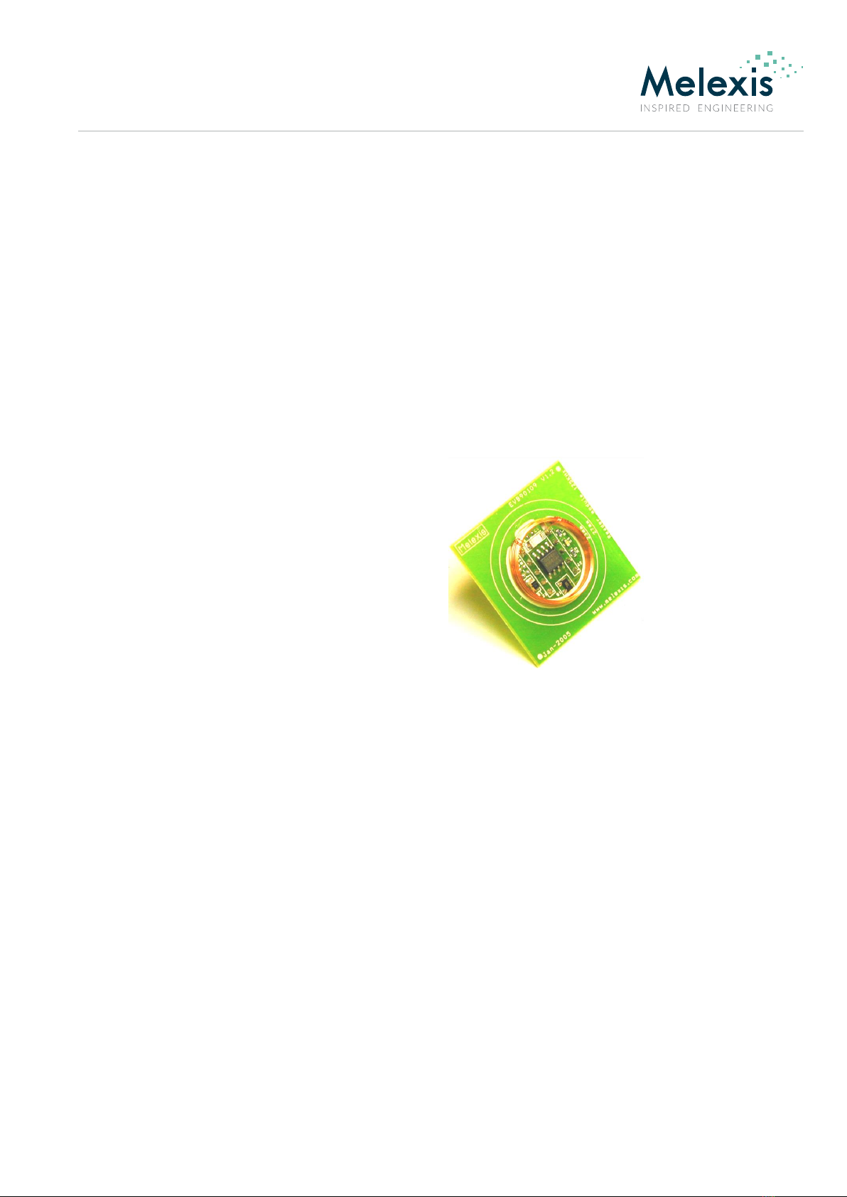
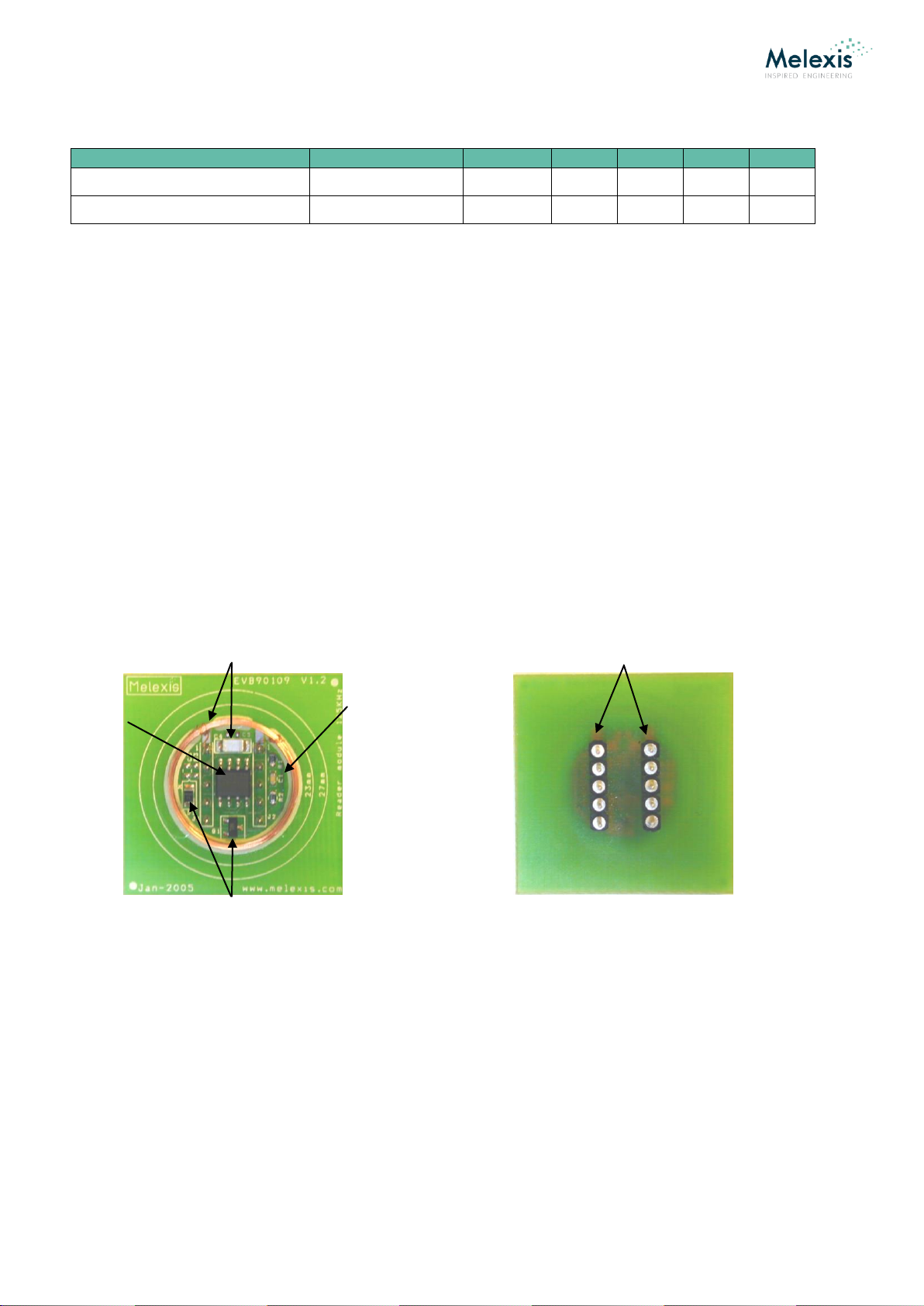
Figure 1: EVB90109
Note: The EVB90109 does not include any pull-up resistors on the digital connections DATA and CLOCK. This must
be done externally, by configuring the IO ports of a microcontroller in pull-up mode, or by adding two external
resistors connected between the digital pins and Vdd.
Parallel resonant antenna (L, C4, C5)
Fast decay circuit (Q1,
D1)
MLX90109
Modulation Network (R1, R2)
Connector DIL-10

EVB90109
MLX90109 Evaluation Board Manual
Page 4 of 10
REVISION 006 - JUNE 20, 2017
390129010901
2.2. Parallel antenna
The parallel antenna of the EVB90109 consists of the inductance (L) of the reader coil and the tune capacitor (C4),
which form a resonant system at 125 kHz with a total (inductance and capacitance) antenna impedance of about
1.3kOhms. The MLX90109 is specified to drive a minimal antenna impedance of 1kOhm, which can be
theoretically calculated using the following formula.
rresantant LQZ
Care should be taken that the presence of a transponder may reduce the theoretical antenna impedance to be
smaller that the minimum specified. Therefore it may be of interest to take some extra margin in the antenna
design by taking a slightly higher quality factor to increase the antenna impedance.
A tune capacitance with a poor quality factor may also reduce the global performances of the antenna, as shown
in the following formula.
CLant QQQ //
Therefore, the tune capacitance should be taken with a high quality factor or low ESR (plastic or mica) to not
reduce the total impedance of the antenna and moreover, to not annihilate all the efforts made in the design of
the antenna to work with a high quality factor and then to get the maximum of operating distance.
2.3. Modulation network
The modulation network is used to set the voltage on the MODU pin of the MLX90109. As shown in the following formula,
the voltage on the antenna can be adjusted according to this voltage. This feature can be used to reduce the power
consumption of the chip by setting a lower voltage on the antenna. Under no circumstances it can be used to make
proportionnal modulaiton, due to internal feedback loop which doesn’t allow this use.
overshootMODUDDant VVVV
The EVB90109 is provided with two resistors R1 and R2 as the modulation netwok controlled through the pin MODUR2 to
set the voltage on the antenna respectively On (Vmodu to 0.8 Volts) and Off (Vmodu to 5 Volts). Others footprint C1, C3 and
R3 and an extra pin MODUR3 are available on the board and can be used for specific applications.
2.4. Antenna voltage in read operation
The resistors R1 and R2 set VMODU to 0.8V (1V for full temperature range [–40, 85] C) which is the lowest possible voltage
to guarantee that the antenna driver of the MLX90109 stays out of its linear operating zone. The field is set On (VMODU to
0.8V) and Off (VMODU to VDD) when applying 0V and VDD on pin MODUR2.

EVB90109
MLX90109 Evaluation Board Manual
Page 5 of 10
REVISION 006 - JUNE 20, 2017
390129010901
2.5. Noise cancellation in read operation
The resonant antenna is a natural band-pass filter, which becomes more effective as Qant increases.
The MLX90109 has an internal first order filtering of the envelope that changes according to the setting of the SPEED pin to
fit to the biphase and Manchester data spectrum:
2kbaud (speed = 1): 400Hz to 3.6kHz
4kbaud (speed = 0): 800Hz to 7.2kHz
Noise that is injected on MODU pin or on VDD will cause Vant to change, and will therefore be considered to be data by the
sampler.
This noise can simply be cancelled by adding a capacitor C1 between MODU and VDD. Together with the modulation
network R1 and R2, it creates a high pass filter with cut off frequency at:
121 //21CRR
Note: Due to the long time constant introduces and the parasitic oscillations that it may provoke with the transistor Q1, the
capacitor C1 must be removed when using the EVB90109 in On/Off keying modulation mode.
2.6. Antenna voltage in 100% modulation operation
The modulation network R1 and R2 can be used to set the voltage amplitude on the antenna On and Off by applying 0 Volts
and Vdd on the pin MODUR2.
Switching ON the magnetic field depends on the internal driver of MLX90109 and takes less than 5 carrier periods. Switching
OFF the magnetic field depend on the quality factor (Qant) of the parallel antenna connected to the reader (about 24
periods with the EVB90109). To reduce this fall time, the “fast decay” circuit can be used.
EVB90109
MLX90109 Evaluation Board Manual
Page 6 of 10
REVISION 006 - JUNE 20, 2017
390129010901
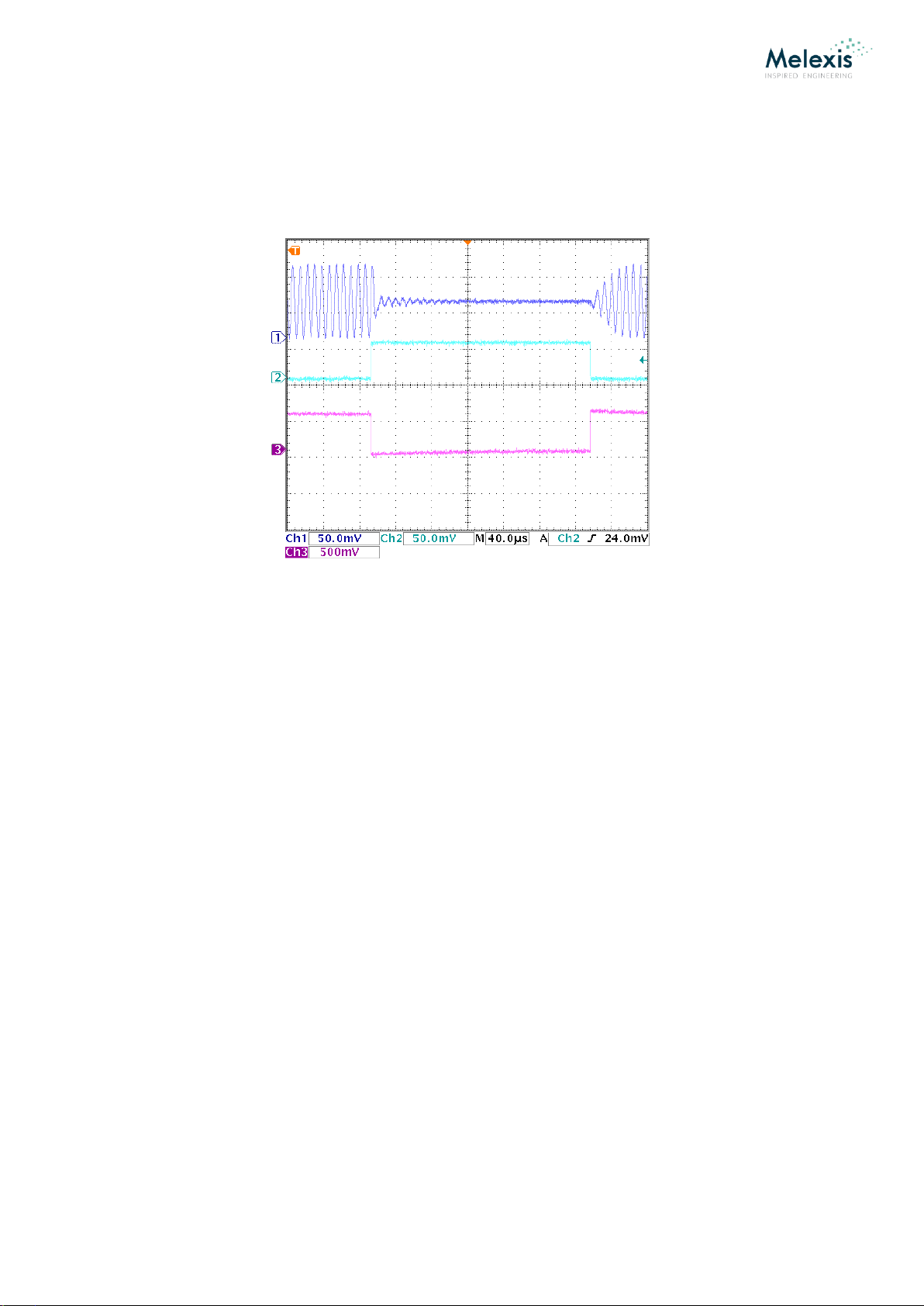
2.7. Fast decay circuit
Very small fall time may be required in fast protocol, to be understood by the transponder in the field. This is why, the
EVB90109 include a “fast decay” circuit controlled through the pin FAST_DECAY and composed of the transitstor Q1 and the
diode D1. The following picture shows how to implement the “fast decay” system.
Picture 1: Fast Decay module control, (1) Antenna, (2) MODUR2, (3) FAST_DECAY

EVB90109
MLX90109 Evaluation Board Manual
Page 7 of 10
REVISION 006 - JUNE 20, 2017
390129010901
3. Schematic
The following diagram shows the schematic of the EVB90109. All components in grey are not mounted but the footprints are
present if the user wants to use it for dedicated applications.
1 8
7
6
5
2
3
4
MLX90109
VDD
VDD L
C
R1
C1
R2 R3 C3
COIL
VSS
SPEED
MODE
CLOCK
DATA
VDD
MODUR3
MODUR2
1
2
3
5
6
7
8
9
10
D1 Q1
4Fast_Decay
Figure 2: Schematic of the EVB90109

EVB90109
MLX90109 Evaluation Board Manual
Page 8 of 10
REVISION 006 - JUNE 20, 2017
390129010901
4. Physical outline
The following figure shows the outline of the MLX90109 evaluation board.
Figure 3: EVB90109 outline: top side
R2
C1
R1
R3
C3
D1
C4
Q1
MLX90109
Coil
DIL-10
DIL-10
1
2
3
4
5
10
9
8
7
6
EVB90109
MLX90109 Evaluation Board Manual
Page 9 of 10
REVISION 006 - JUNE 20, 2017
390129010901
5. Pinning of the EVB90109
Pin number DIL-10
Name
Description
1
COIL
Oscillator Output
2
VSS
Ground
3
SPEED
Data rate selection
4
FAST_DECAY
Fast decay circuit control
5
MODUR3
Modulation Network
6
MODUR2
Modulation Network
7
MODE
Decoding selection
8
CLOCK
Clock signal
9
DATA
Decoded data
10
VDD
Power Supply
Table 2: Pinning of the EVB90109
6. Components
Reference
Value
Description
R1
39 kohms
Modulation network
R2
8.2 kohms
Modulation network
R3
Not mounted
Additional resistor for the modulation network
C1
Not mounted
Noise cancellation capacitance
C2
Not mounted
Additional capacitance for the modulation network
C3
Not mounted
Additional capacitance for the modulation network
C4
22nF
Tune capacitance
Table 3: Components
Reference
Value1)
Units
Description
L1
73.7
µH
Coil inductance
Qant
25
Coil quality factor
Zant
1447
kOhm
Antenna Impedance, calculated = ω0*Lant*Qant
Table 4: Reader Coil L1 Electrical Specifications
Reference
Value1)
Units
Description
H
3
mm
Coil height
OD
18.9
mm
Outside diameter
ID
Number of turns
17
mm
Inside diameter
Nr
52
-
Number of turns
Table 5: Reader Coil L1 Physical Specifications
1) Typical value at 125kHz

EVB90109
MLX90109 Evaluation Board Manual
Page 10 of 10
REVISION 006 - JUNE 20, 2017
390129010901
7. Contact
For the latest version of this document, go to our website at www.melexis.com.
For additional information, please contact our Direct Sales team and get help for your specific needs:
Europe, Africa
Telephone: +32 13 67 04 95
Email : sales_europe@melexis.com
Americas
Telephone: +1 603 223 2362
Email : sales_usa@melexis.com
Asia
Email : sales_asia@melexis.com
8. Disclaimer
The information furnished by Melexis herein (“Information”) is believed to be correct and accurate. Melexis disclaims (i) any and all liability in connection with or arising out of the
furnishing, performance or use of the technical data or use of the product(s) as described herein (“Product”) (ii) any and all liability, including witho ut limitation, special,
consequential or incidental damages, and (iii) any and all warranties, express, statutory, implied, or by description, including warranties of fitness for particular purpose, non-
infringement and merchantability. No obligation or liability shall arise or flow out of Melexis’ rendering of technical or other services.
The Information is provided "as is” and Melexis reserves the right to change the Information at any time and without notice. Therefore, before placing orders and/or prior to
designing the Product into a system, users or any third party should obtain the latest version of the relevant information to verify that the information being relied upon is current.
Users or any third party must further determine the suitability of the Product for its application, including the level of reliability required and determine whether it is fit for a
particular purpose.
The Information is proprietary and/or confidential information of Melexis and the use thereof or anything described by the In formation does not grant, explicitly or implicitly, to
any party any patent rights, licenses, or any other intellectual property rights.
This document as well as the Product(s) may be subject to export control regulations. Please be aware that export might require a prior authorization from competent authorities.
The Product(s) are intended for use in normal commercial applications. Unless otherwise agreed upon in writing, the Product(s) are not designed, authorized or warranted to be
suitable in applications requiring extended temperature range and/or unusual environmental requirements. High reliability applications, such as medical life-support or life-
sustaining equipment are specifically not recommended by Melexis.
The Product(s) may not be used for the following applications subject to export control regulations: the development, product ion, processing, operation, maintenance, storage,
recognition or proliferation of 1) chemical, biological or nuclear weapons, or for the development, production, maintenance o r storage of missiles for such weapons: 2) civil
firearms, including spare parts or ammunition for such arms; 3) defense related products, or other material for military use or for law enforcement; 4) any applications that, alone
or in combination with other goods, substances or organisms could cause serious harm to persons or goods and that can be used as a means of violence in an armed conflict or any
similar violent situation.
The Products sold by Melexis are subject to the terms and conditions as specified in the Terms of Sale, which can be found at https://www.melexis.com/en/legal/terms-and-
conditions.
This document supersedes and replaces all prior information regarding the Product(s) and/or previous versions of this document.
Melexis NV © - No part of this document may be reproduced without the prior written consent of Melexis. (2016)
ISO/TS 16949 and ISO14001 Certified
This manual suits for next models
1
Table of contents
Other Melexis Motherboard manuals


