Pericom Semiconductor Corp., 3545 N. First Street, San Jose, California, USA 408-435-0800 www.pericom.com
Page 10
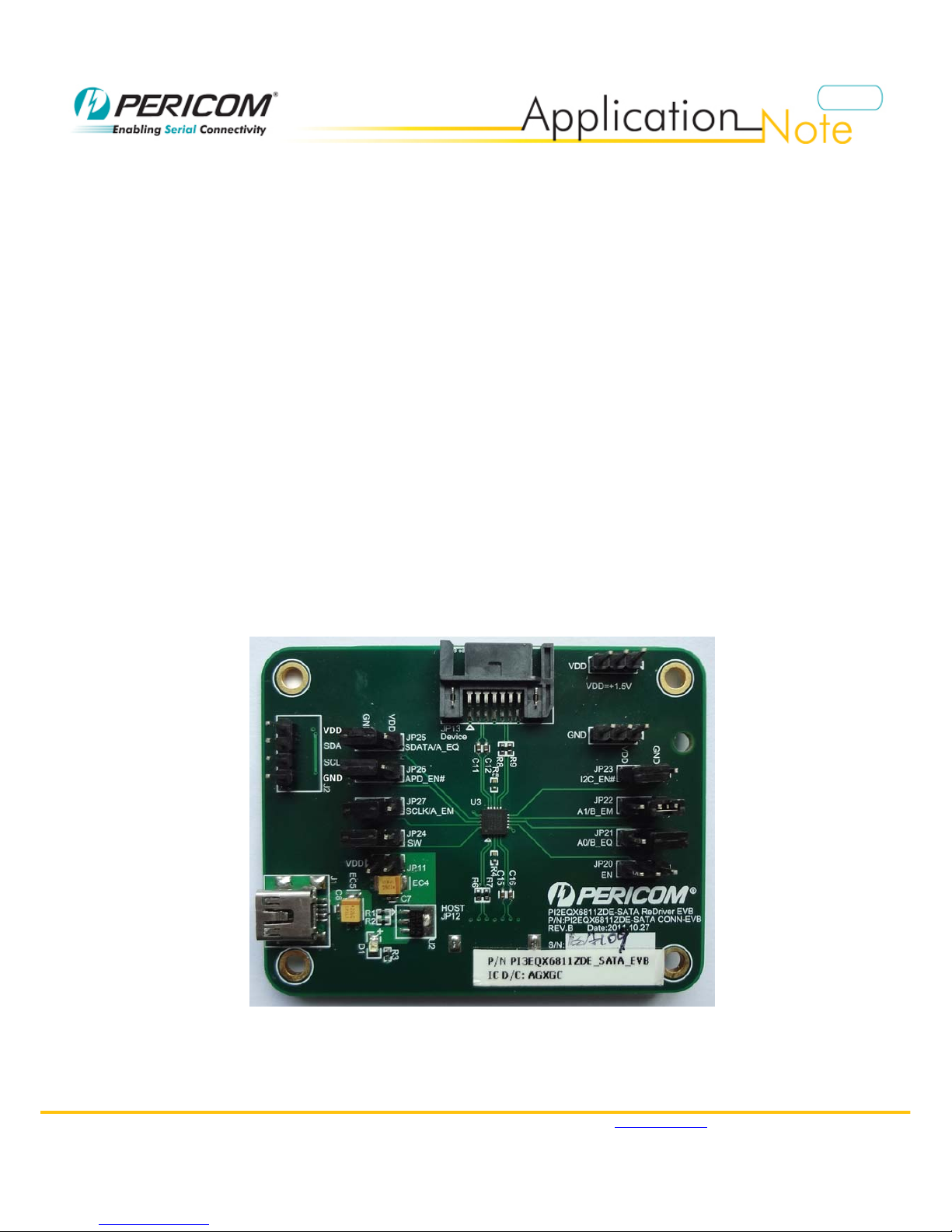
zPCB BOM List
Reference Description Package Qty
U2 LM3674-1.5V SOT23-5 1
U3 PI2EQX6811ZDE@TQFN20 TQFN20 1
Bare PCB
PCB, PI2EQX6811ZDE-SATA ReDriver
Rev.B PCB 1
D1 LED 0805 1
JP12,JP13 SATA L-type connector L-type 2
J2 4p-2.54mm Connector 2.54mm 1
J1 miniUSB connector B-type 1
JP11 2PIN HEADER 2.54mm 1
JP18,JP19,JP20,JP21,JP22,
JP23,JP24,JP25,JP26,JP27 3PIN HEADER 2.54mm 10
C11,C12,C15,C16 Ceramic Capacitor, 10nF 0402 4
C1,C2,C3,C4,C6,C7,C8 Ceramic Capacitor, 0.1uF 0402 7
EC1,EC4,EC5 Tan cap, 22u 3528 3
R3 Chip Resistor, 510ohm 0402 1
R29,R30 Chip Resistor, 10Kohm 0402 2
R1,R6,R7,R8,R9 Chip Resistor, 0ohm 0402 5


 User manual")


