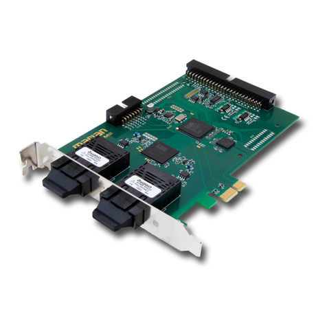
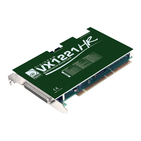
Merging Mykerinos User manual

Mykerinos
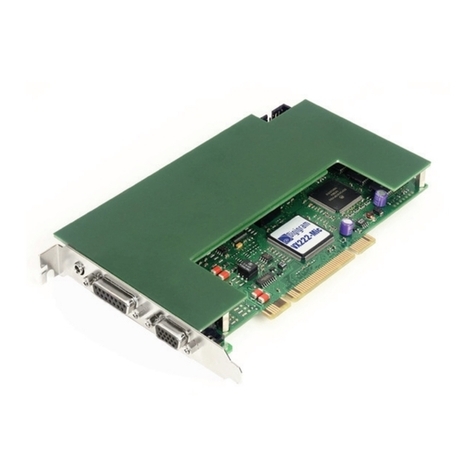
The Audio Processing Board
User Manual
Version: DOC-2.11 (December 2006)
©2001-2006 Merging Technologies
Merging Technologies
Le Verney, CH-1070 Puidoux Switzerl nd
Tel: +41 21 946 04 44 ● F x: +41 21 946 04 45
www.merging.com

- 2 -
1 IMPORTANT NOTICE:
Please read the following information very carefully before attempting any installation. Failure to comply with the
precise instructions may result in damage to your Merging hardware. Please read this entire section of the manual
carefully before installation.
1.1 STATIC DANGER NOTICE:
Please note that the Mykerinos board contains delicate electronic components that can be damaged or even destroyed
when exposed to static electricity. Take all necessary precautions not to discharge static electricity when touching any
of the Mykerinos components.
1.2 INFORMATION FOR THE USER:
Mykerinos nd its d ughter c rd comply with the following specific tions:
MC missions
EN 55022 : 1994 /A1 : 1995 /A2 : 1997 Cl ss A ITE emissions requirements (EU)
FCC 47 CFR P rt 15 Cl ss A emissions requirements (USA)
MC Immunity
EN 50082-1: 1992 EMC residenti l, commerci l nd light industri l generic immunity st nd rd.
FCC Notice
This product h s been tested nd found to comply with the limits for Cl ss A digit l device, pursu nt to P rt 15 of the FCC
rules. Oper tion is subject to the following two conditions: (1) This device m y not c use h rmful interference, nd (2) This
device must ccept ny interference received, including interference th t m y c use undesired oper tion.
These limits re designed for providing re son ble protection g inst h rmful interference in residenti l inst ll tion. This
equipment gener tes, uses nd c n r di te r dio frequency energy nd, if not inst lled nd used in ccord nce with the
instructions cont ined in this m nu l, m y c use h rmful interference to r dio nd television communic tions. However,
there is no gu r ntee th t interference will not occur in p rticul r inst ll tion.
NOTE: Connecting this device to peripher l devices th t do not comply with CLASS A requirements or using n unshielded
peripher l d t c ble could lso result in h rmful interference to r dio or television reception. The user is c utioned th t ny
ch nges or modific tions not expressly pproved by the p rty responsible for compli nce could void the user’s uthority to
oper te this equipment. To ensure th t the use of this product does not contribute to interference, it is necess ry to use
shielded I/O c bles.
C Notice
Such m rking is indic tive th t this system’s devices meet the following pplic ble technic l st nd rds:
•EN 55022 – “Inform tion Technology Equipment - R dio disturb nce ch r cteristics Limits nd methods of
me surement”
•EN 50082-1: 1992 – “Electrom gnetic comp tibility – Generic immunity st nd rd P rt 1:Residenti l, commerci l, nd
light industry”
This product is cl ssified for use in typic l Cl ss A commerci l environment, nd is not designed or intended for use in
other EMC environments. The user of this product is obliged for proper use nd inst ll tion of the product nd for t king ll
steps necess ry to remove sources of interference to telecommunic tions or other devices.

- 3 -
2 Mykerinos Warranty Information
This product is w rr nted to be free of defects in m teri ls nd workm nship for period of one ye r from the d te of
purch se. Merging Technologies, Inc. extends this Limited W rr nty to the origin l purch ser.
In the event of defect or f ilure to confirm to this Limited w rr nty, Merging Technologies, Inc. will rep ir or repl ce the
product without ch rge within sixty (60) d ys. In order to m ke cl im under this limited w rr nty, the purch ser must
notify Merging Technologies, Inc. or their represent tive in writing, of the product f ilure. In this limited w rr nty the
customer must upon Merging Technologies, Inc. request, return the product to the pl ce of purch se, or other loc l
design tion, for the necess ry rep irs to be performed. If the consumer is not s tisfied with the rep ir, Merging Technologies,
Inc. will h ve the option to either ttempt further rep ir, or refund the purch se price.
This w rr nty does not cover: (1) Products which h ve been subject to misuse, buse, ccident, physic l d m ge, neglect,
exposure to fire, w ter or excessive ch nges in the clim te or temper ture, or oper tion outside m ximum r ting. (2) Products
on which w rr nty stickers or product seri l numbers h ve been removed, ltered or rendered illegible. (3) The cost of
inst ll tions, remov l or reinst ll tion. (4) D m ges c used to ny other products.

- 4 -
3 Table of Contents
1
IMPORTANT NOTIC : ............................................................................................................................................... 2
1.1
STATIC
DANGER
NOTICE:.................................................................................................................................... 2
1.2
INFORMATION
FOR
THE
USER:........................................................................................................................... 2
2
MYK RINOS WARRANTY INFORMATION.......................................................................................................... 3
3
TABL OF CONT NTS ............................................................................................................................................... 4
4
INTRODUCTION .......................................................................................................................................................... 6
5
MYK RINOS F ATUR S OV RVI W ................................................................................................................... 6
6
MYK RINOS BLOCK DIAGRAM............................................................................................................................. 7
6.1
M
YKERINOS
B
LOCK
D
IAGRAM
................................................................................................................................... 7
6.2
M
YKERINOS
O
N
-B
OARD
C
ONNECTORS AND
J
UMPERS
................................................................................................ 7
6.3
M
YKERINOS BRACKET VIEW
....................................................................................................................................... 8
7
SYNC F ATUR S ......................................................................................................................................................... 9
7.1
S
IGNAL
D
ESCRIPTION
................................................................................................................................................. 9
7.1.1
CVS1 IN............................................................................................................................................................ 9
7.1.2
WCKIO (Old CVS2In) .................................................................................................................................... 10
7.1.3
CVS OUT........................................................................................................................................................ 10
7.1.4
LTC IN ............................................................................................................................................................ 10
7.1.5
LTC OUT ........................................................................................................................................................ 10
7.2
B
REAKOUT
C
ABLE
P
IN
-
OUT DESCRIPTION
(J2) ......................................................................................................... 11
7.3
V
IDEO
/TC
H
EADER
P
IN
-
OUT DESCRIPTIONS
(JP2) .................................................................................................... 12
8
MONITORING H ADPHON F ATUR S (J3) .................................................................................................... 13
8.1
M
ONITORING OUTPUT CHARACTERISTICS
................................................................................................................. 13
9
MYK RINOS MODULAR I/O DAUGHT R CARDS............................................................................................ 14
9.1
ADAT
I/O
D
AUGHTER
C
ARD
................................................................................................................................... 14
9.1.1
Optical I O configuration ............................................................................................................................... 15
9.1.1.1
Standalone mode (also called Mono-board mode) ............................................................................... 15
9.1.1.2
HDTDM mode....................................................................................................................................... 15
9.1.1.3
XDTDM mode (from Pyramix v. 5.0 and higher).................................................................................. 15
9.2
MADI
I/O
D
AUGHTER
C
ARDS
-
I
NCLUDING VERSION
II ........................................................................................... 16
9.2.1
Coaxial MADI version connector view........................................................................................................... 16
9.2.1.1
Coaxial Cable Specifications ................................................................................................................ 16
9.2.2
Optical MADI version connector view ........................................................................................................... 17
9.3
AES-EBU,
SDIF,
TDIF
I/O
D
AUGHTER
C
ARD
......................................................................................................... 17
9.3.1
AES-EBU without SRC ................................................................................................................................... 18
9.3.2
AES-EBU with SRC on 8 channels ................................................................................................................. 18
9.3.3
SDIF ............................................................................................................................................................... 18
9.3.4
TDIF ............................................................................................................................................................... 18
9.4
DUAL
D
AUGHTER
C
ARD
.......................................................................................................................................... 19
9.4.1
Card Features................................................................................................................................................. 19
9.4.2
Front connector .............................................................................................................................................. 20
9.4.3
Rear 0 connector ............................................................................................................................................ 20
9.5
B
REAKOUT CABLE CONNECTORS FOR
AES,
SDIF,
TDIF
AND
DUAL
DAUGHTER CARDS
......................................... 21
9.5.1
Analog I O breakout cable – Only for the DUAL daughter card .................................................................. 21
9.5.2
AES EBU I O breakout cable ......................................................................................................................... 21

- 5 -
10
TYPICAL AUDIO CONN CTIONS B TW N DUA II & MYK RINOS........................................................ 22
10.1
A
UDIO FOR
V
IDEO WITH
SONY
D
IGITAL
B
ETA
C
AM
U
SERS
................................................................................... 22
10.2
A
UDIO FOR
V
IDEO WITH
SONY
A
NALOG
B
ETA
C
AM
U
SERS
................................................................................... 23
10.3
M
ERGING
T
ECHNOLOGIES
P
YRAMIX
4.
X
DAW
WITH
S
URROUND
M
ONITORING
..................................................... 24
11
TYPICAL AUDIO CONN CTIONS B TW N SPHYNX & MYK RINOS .................................................... 25
11.1
A
UDIO FOR
V
IDEO WITH
SONY®
D
IGITAL
B
ETA
C
AM
U
SERS
................................................................................ 25
11.2
A
UDIO FOR
V
IDEO WITH
SONY®
A
NALOG
B
ETA
C
AM
U
SERS
................................................................................ 26
11.3
M
ERGING
T
ECHNOLOGIES
P
YRAMIX
4.
X
DAW
S
ETUP
............................................................................................ 27
12
MYK RINOS POW R CONSUMPTION ............................................................................................................... 28
12.1
M
YKERINOS MOTHERBOARD
(
ALONE
)..................................................................................................................... 28
12.2
ADAT
DAUGHTER CARD
......................................................................................................................................... 28
12.3
MADI
1
DAUGHTER CARD
....................................................................................................................................... 28
12.4
MADI
2
DAUGHTER CARD
....................................................................................................................................... 29
12.5
AES-EBU
DSD
(
W
/
O
SRC)
DAUGHTER CARD
........................................................................................................ 29
12.6
AES-EBU
SRC
DAUGHTER CARD
........................................................................................................................... 29
12.7
SDIF
OR
TDIF
DAUGHTER CARD
............................................................................................................................. 29
12.8
DUAL
(A
NALOG
–
AES/EBU)
DAUGHTER CARD
.................................................................................................... 29
13
CONTACTING M RGING ....................................................................................................................................... 30

- 6 -
4 Introduction
This document presents nd describes the third gener tion Merging h rdw re/softw re solution, PCI b sed, high
perform nce, cost effective udio processing c rd n med MYKERINOS.
5 Mykerinos Features Overview
Mykerinos is Merging's nswer to cre te le ding edge high perform nce udio processing c rd solution. It builds upon over
6 ye rs of experience designing nd m nuf cturing PC b sed Audio C rds nd incorpor tes hundreds of users feedb cks into
comp ct third gener tion flexible solution.
Here is quick summ ry of fe tures:
•PCI V2.1 compli nt. Supports both 5 Volts nd 3.3 Volts PCI environments
•Driver support for Windows XP / 2000 / NT 4
•Very cost effective
•B sed on 2
nd
gener tion Philips Trimedi 32 bit flo ting point processing VLIW technology
•High Perform nce (upto > 400 MFlops sust ined, 800 MB/s SDRAM interf ce, etc.)
•Support for ll s mpling r tes from 32 kHz up to 192 kHz, s well s DSD nd DXD.
•Open Plug-In ( ll C-code) rchitecture supporting Surround-sound nd DVD form ts
•Highly flexible modul r I/O rchitecture c n be t ilored to user's needs by the use of dedic ted d ughter bo rds.
This I/O modul rity offers unique opportunity to meet wide r nge of m rket requirements
•Current Audio I/O d ughter c rd options include ADAT - S/PDIF, MADI, AES/EBU, TDIF, SDIF nd DUAL
•On bo rd Sync Connector, which includes Video Sync I/O re dy for HDTV, VITC re der nd gener tor, LTC
re der nd gener tor nd built-in time code insertion into Video window.
•2 ch nnel 24 bit 96 kHz on-bo rd monitoring output
•Very high perform nce c rd c p ble of high tr ck pl yb ck (up to 64 tr cks) nd v st I/O c p bilities (up to 64
ch nnels)
•Multiple c rds interconnected through XDTDM (eXtreme Definition Time Dom in Multiplex) bus with support of
up to 512 udio ch nnels

- 7 -
6 Mykerinos Block Diagram
6.1 Mykerinos Block Diagram
SSI
SDRAM
Up to 32 MB
Trimedia
TM-1300
PLL
Video
Control Signals only DIFFERENT SIGNALS
MINI DIN
8 POS.
Figure 1 - Mykerinos Block Diagram
The Mykerinos bo rd is b sed on the Philips Trimedi TM-1300 Chip nd its ssoci ted SDRAM running t 144 MHz. The
other peripher ls re:
•1 FPGA (Field Progr mm ble G te Arr y), used to m n ge the control sign ls
•1 Timecode re der – gener tor (LTC nd VITC)
•1 Video PLL, used to lock to ny incoming Video reference such s bl ck-burst PAL, NTSC or Tri-level HDTV
•1 stereo 24 bit 96kHz D/A for onbo rd udio monitoring.
Up to 64 udio ch nnels re conveyed over the Trimedi high-speed “Video IN” nd “Video OUT” buses through connector
J4 to/from the specific I/O d ughter c rd.
6.2 Mykerinos On-Board Connectors and Jumpers
The connectors implemented on the Mykerinos bo rd re s follows:
•JP1 - he der 1x2, Reserved.
•JP2 - Video/TC connector 8x2, offering the s me function lities s J2 but for intern l connection
•JP3 - he der 1x2, used to connect intern lly Video Reference Sync (in lieu of CVS1IN sign l)
•J2 - 1 mini Din 8 pins, used to tr nsfer Video nd Timecode sign ls
•J3 - 1 stereo he dphone monitoring output 3.5mm mini-j ck connector
•J4 - 1 mezz nine connector 32x2, used to connect I/O d ughter c rds
•JP4 - 75ohm termin tion for CVS1IN (input from J2, JP2 or JP3)
•JP5 - 75ohm termin tion for WCKIO (input from J2 or JP2)
•JP6 - monitoring g in ttenu tion (-12dB when open) for the left ch nnel
•JP7 - monitoring g in ttenu tion (-12dB when open) for the right ch nnel

- 8 -
Figure 2 - Connectors & Jumpers layout
Refer to the “Sync Fe tures” nd “Monitoring He dphone Fe tures” ch pters for ddition l inform tion.
6.3 Mykerinos bracket view
The following picture shows view of the PCI br cket with the monitoring j ck nd the mini-Din connectors.
Figure 3 - Mykerinos Bracket with Jack & mini-Din connectors
U20 U19
U14
U11
U16
U17
U15
U21
U22
Q2 Q1
U7
D1
J2
J3
JP2 J4
JP1
JP3
JP4
JP5
JP7
JP6
Monitoring jack
output (J3) Mini-Din connector
for the Video/TC
Breakout cable (J2)

- 9 -
7 Sync Features
Provision for ll Video/TC rel ted sign ls (VITC, LTC, nd Video Sync) is both on 8-pin Mini-Din connector (for extern l
connection) nd on 16-pin he der (for intern l connection). The Video Out c n lso serve s VITC output nd/or TC burn-
in output.
The Mykerinos bo rd supports ll st nd rd Video form ts such s PAL/NTSC, nd ll Tri-level HDTV form ts s
reference synchroniz tion source. VITC c n only be extr cted from st nd rd video form ts. Here re the different
possibilities offered by either the Video/TC br cket or bre kout c ble:
•NTSC/PAL/VITC Video Reference Input + HDTV reference sync source Input
•NTSC/PAL/VITC Video 2 Input or Wordclock I/O
•NTSC/PAL/VITC Video Output
•LTC (SMPTE/EBU) Timecode Input (b l nced, nomin l 2 Vp-p)
•LTC (SMPTE/EBU) Timecode Output (unb l nced, progr mm ble level)
The bre kout c ble llows Mykerinos to lock to video “house sync” or Wordclock reference, re d & gener te VITC nd
re d & gener te LTC. This option lso dds the c p bility to "burn" Time code "insert" in the video output sign l.
This interf ce h s provision for one BNC input CVS1In, one BNC output CVS Out, one BNC input/output WCK, one XLR
Fem le for LTC input nd one XLR M le for LTC output.
This interf ce is quite simil r in function lity to the Video/TC br cket option. The m in difference is in the video loop
through mode, which is not v il ble with the bre kout c ble.
7.1 Signal Description
7.1.1 CVS1 IN
This input ccepts composite PAL/NTSC or Tri-level HDTV video sign l th t c n be used by Mykerinos to lock its udio
s mpling r te to video reference. The CVS1 input should be used for the m in “house sync” or "bl ck-burst" reference
video sign l. It is lso possible to use this input s VITC source (only st nd rd PAL nd NTSC r tes).
Historic lly ll the Mykerinos bo rds were shipped with jumper JP4 closed, which ctiv tes the 75Ω video termin tion on
CVS1IN sign l. Dated from Mid-April 2006, Merging has decided to ship all the Mykerinos boards with JP4 open
(MB1 S/N 15489 - …, MB2 S/N 13364 - … nd MB5 S/N 17449 - …).
See below n extr ct of the ECO MYK013 for technic l det iled expl n tion:
“Historically all the Mykerinos boards were shipped with jumper JP4 closed, which activates the 75Ω video termination on
CVS1IN signal.
Exception was made when a Mykerinos board is integrated into a Merging Workstation (Pyramix or VCube). In that case,
this jumper is left open by Merging to avoid a double video termination, one on the Mykerinos board (JP4) and one on the
chassis rear panel (switch).
Then, on most cases, the integration of the Mykerinos board into a Merging Workstation is left to the discretion of the
Dealers themselves or to an official assembly sub-contractor.
As many persons may be involved in this process, an error on JP4 may occur at different moments between the final
assembly process, the shipment department, and the integration into the Merging Workstation.
Due to the increasing percentage of Mykerinos boards integrated in a Merging chassis since 2005 and to avoid a double
termination on JP4, Merging has decided to ship all the Mykerinos boards (from serial numbers indicated above) with JP4
open, without differentiation if the boards will be integrated into a Merging Workstation or not. The jumper will be present
but only attached to one pin of the JP4 connector.
Consequently, all the chain process will be drastically simplified, involving only the final assembly department and thus,
avoiding any future problems.”

- 10 -
7.1.2 WCKIO (Old CVS2In)
This connector c n be used, under softw re control, in 2 modes: Wordclock IN or Wordclock OUT.
When softw re configured s WCK Input it ccepts n extern l Wordclock reference sign l between 0.2 nd 5 Vp-p. When
softw re configured s WCK Output it provides 5 V TTL-comp tible sign l with 22-Ohm output imped nce.
Note: whenever used with Wordclock sign l (either Input or Output), do not termin te (JP5 open) on Mykerinos nd on the
Video/TC br cket (This is the def ult f ctory settings).
Note, th t historic lly, this connector w s ble to input Video sign l, s well. The following modific tion h s been m de,
d ted from November 2004: The Video input feature has been removed from CVS2In/WCK signal. The Wordclock I/O
capability remains unchanged. This modific tion pplies to the following Mykerinos bo rds: MB1 S/N 12600 - … nd
MB5 S/N 16150-16759 nd 16803 - ….
See below n extr ct of the ECO MYK011B for technic l det iled expl n tion:
“
When too high a voltage is applied to the Video 2 input (CVS2IN-WCKI O), the Video sub-system of the Mykerinos card may enter into an
unstable state (latch up) and subsequently corrupt the proper decoding of the Video 1 Input signal (CVS1IN) as well as the Video Output
signal (CVSOUT). This is specifically the case when CVS2IN is used as a word clock I O. The Video TC handling sub-unit on the
Mykerinos card may be triggered to enter this latch-up state with as little as a full 5 Volt p-p Wordclock signal applied.
To resolve this issue permanently, the solution is to physically remove the path linking the CVS2IN-WCKI O to the Video TC circuitry and
disconnect this input from the Video sub-system by removing the C127 capacitor to prevent any signal to enter into the Time code chip
(U10). This modification does not prevent to use the Word clock I O feature but removes the possibility to use the CVS2IN-WCKI O as a
secondary Video VITC input
”
7.1.3 CVS OUT
This sign l outputs the composite video sign l coming from CVS1IN only. This sign l m y ddition lly c rry VITC nd/or
time code "burn-in" video insert gener ted by Mykerinos.
Note: CVSOUT provides monitoring qu lity video output only nd is not intended to be used s loop through “bl ck
burst” output.
7.1.4 LTC IN
LTC IN is symmetric l input sign l. It ccepts n extern l SMPTE/EBU time code sign l between 0.2 nd 5 Vp-p.
7.1.5 LTC OUT
LTC OUT is n unb l nced output sign l. The output volt ge level c n be softw re djusted from 0V to 2.5V p-p.

- 11 -
E
c
h
.
M
e
r
g
i
n
g
T
e
c
h
n
o
l
o
g
i
e
s
M
i
n
i
D
I
N
C
a
b
l
e
(
8
p
i
n
s
)
1
2
3
X
L
R
3
-
M
L
T
C
O
U
T
1
2
3
X
L
R
3
-
F
L
T
C
I
N
B
N
C
-
M
C
V
S
1
I
N
B
N
C
-
M
C
V
S
2
/
W
C
K
I
N
B
N
C
-
M
C
V
S
O
U
T
M
i
n
i
D
I
N
8
p
A
l
l
c
o
n
n
e
c
t
o
r
s
s
e
e
n
f
r
o
m
t
h
e
r
e
a
r
P
l
u
g
M
a
l
e
3
1
4
5
2
6
7
8
T
o
t
a
l
l
e
n
g
t
h
:
1
0
0
c
m
S
p
l
i
t
l
e
n
g
t
h
:
8
0
c
m
1
3
4
5
2
6
7
8
L
e
V
e
r
n
e
y
C
H
-
1
6
0
4
P
u
i
d
o
u
x
D
.
B
a
u
d
a
t
M
O
L
D
I
N
G
S
T
R
A
I
N
R
E
L
I
E
F
B
o
l
d
T
e
x
t
=
T
e
x
t
o
n
L
a
b
e
l
7.2 Breakout Cable Pin-out description (J2)
The following picture describes the physic l implement tion of the sign ls on the mini Din m le plug of the bre kout c ble.
Figure 4 - Breakout Cable Pin-out

- 12 -
7.3 Video/TC Header Pin-out descriptions (JP2)
The pins on the Video/TC he der re s described below:
Figure 5 - Video TC Header Pin-out
When the Video/TC He der is used, be sure to not termin te twice the CVS1IN input. Use only either the termin tion on the
Mykerinos bo rd (JP4) or this provided on the Video/TC He der.
Note th t CVS2IN is not v il ble on the Mykerinos bo rd since November 2004 (MB1 S/N 12600 - … nd MB5 S/N
16150-16759 nd 16803 - …).
Here is represent tion of the Video/TC br cket:
Figure 6 - Video TC bracket
Terminology:
CVS: Composite Video Sign l, NTSC, PAL or HDTV.
LTC: Longitudin l Time Code, either SMPTE or EBU.
VITC: Vertic l Interv l Time Code, either SMPTE on NTSC or EBU on PAL.
SCL, SDA: Seri l clock nd Seri l D t for I2C seri l communic tion
Sp re 2
ASC Out
TXD
Sp re 1
GND
CVS Out
LTC Out
SCL
ATC Out
500mA fused +5v
RXD
GND
CVS2/WCLK In & Out
CVS1 In
LTC In
SDA
PCB
Component side
CVS Out
CVS In 1
Wordclock In & Out (Old
CVS2In)
LTC In
LTC Out
He der 1
He der 2
Jumpers
16-pin
ribbon c ble

- 13 -
8 Monitoring Headphone Features (J3)
The monitoring output is b sed on stereo 96kHz / 24 bit D/A (unb l nced). The output level is softw re controlled.
Mykerinos revision D nd bove fe ture 2 new jumpers JP6 nd JP7 on the left nd right ch nnels respectively. Opening
these jumpers results in 12 dB g in reduction on e ch monitoring ch nnel.
8.1 Monitoring output characteristics
The first gr ph shows the frequency response & the THD+N @ 48kHz nd the second gr ph shows the Noise floor FFT @
48kHz .
Figure 7 - Monitoring frequency response measurement
-130
+30
-120
-110
-100
-90
-80
-70
-60
-50
-40
-30
-20
-10
+0
+10
+20
d
B
u
-130
+30
-120
-110
-100
-90
-80
-70
-60
-50
-40
-30
-20
-10
+0
+10
+20
d
B
u
20
20k
50
100
200
500
1k
2k
5k
10k
Hz
Figure 8 - Monitoring Noise spectrum measurement
-90
+30
-85
-80
-75
-70
-65
-60
-55
-50
-45
-40
-35
-30
-25
-20
-15
-10
-5
+0
+5
+10
+15
+20
+25
d
B
u
-90
+30
-85
-80
-75
-70
-65
-60
-55
-50
-45
-40
-35
-30
-25
-20
-15
-10
-5
+0
+5
+10
+15
+20
+25
d
B
u
20
20k
50
100
200
500
1k
2k
5k
10k
Hz

- 14 -
Optical Input A
Optical Input B
Optical Output A
Optical Output B
Monitoring jack
output Breakout cable
connector
9 Mykerinos Modular I/O Daughter cards
One core fe ture of Mykerinos’ rchitecture is to bre k it into two p rts: the portion th t plugs into the PCI connector of the
PC nd the I/O d ughter c rd th t cont ins the physic l connectors to the outside world. This llows for potenti lly m ny
system pplic tions without committing the design to ny specific I/O configur tions.
9.1 ADAT I/O Daughter Card
This I/O d ughter c rd fe tures two sets of Toslink Optic l connectors e ch c rrying up to eight ch nnels of 24-bit Audio in
the ADAT comp tible form t. This provides up to 16 mono ch nnels of input nd 16 ch nnels of output up to 48kHz nd up
to 8 ch nnels t 96kHz in S/MUX comp tible form t. One of the sets c n be progr mmed in softw re to c rry SPDIF (or
AES-EBU) form tted sign ls inste d of ADAT. In this mode, tot l I/O is limited to 2 + 8 = 10 Digit l Audio ch nnels.
STANDALONE ode co patibility: When running in STANDALONE system, the ADAT I/O d ughter c rd offers 16 I/O
ch nnels in ADAT form t nd/or 2 I/O stereo ch nnels in SPDIF form t (SPDIF nd ADAT modes use the s me optic l
connectors nd re consequently exclusive one with the other).
HDTDM ulti-board ode co patibility: When running in HDTDM multi-bo rd system, the ADAT I/O d ughter c rd
offers udio in ADAT form t ONLY. No SPDIF format is supported.
XDTDM ulti-board ode co patibility: This mode is v il ble from Pyr mix version 5.0 nd higher. When running in
XDTDM multi-bo rd system, the ADAT I/O d ughter c rd c nnot be used for input nd is then only c p ble of 8 ADAT
outputs vi Optic l Output A with the s me 8 duplic ted on Optic l Output B. No SPDIF format is supported.
WARNING! When using the ADAT daughter card in XDTDM mode (from Pyramix version 5.0 and higher) it
requires a hardware modification before being used in XDTDM mode. Without this modification, the use of the board
may result in data loss. Please contact your Merging Technologies Sales Partner to arrange a mod.
The following figure represents the configur tion of the Mykerinos br cket when plugged with n ADAT d ughter c rd.
Figure 9 - Mykerinos & ADAT daughter card connectors

- 15 -
9.1.1 Optical I/O configuration
The following t bles resume the I/O form ts v il ble in e ch mode. These form ts re softw re select ble into Pyr mix.
(A = Optic l A / B = Optic l B)
9.1.1.1 Standalone mode (also called Mono-board mode)
INPUT Modes
A/ ADAT Ch nnel 1 – 8 (A) - ADAT Ch nnel 9 – 16 (B)
B/ SPDIF Ch nnel 1 – 2 (A) - ADAT Ch nnel 9 – 16 (B)
OUTPUT Modes
A/ ADAT Ch nnel 1 – 8 (A) - ADAT Ch nnel 9 – 16 (B)
B/ ADAT Ch nnel 1 – 8 (A) - ADAT Ch nnel 1 – 8 (B)
C/ SPDIF Ch nnel 1 – 2 (A) - ADAT Ch nnel 1 – 8 (B)
D/ SPDIF Ch nnel 1 – 2 (A) - ADAT Ch nnel 9 – 16 (B)
9.1.1.2 HDTDM mode
INPUT Modes
A/ ADAT Ch nnel 1 – 8 (A) - ADAT Ch nnel 9 – 16 (B)
B/ ADAT Ch nnel 1 – 8 (A) - ADAT Ch nnel 1 – 8 (B)
OUTPUT Modes
A/ ADAT Ch nnel 1 – 8 (A) - ADAT Ch nnel 9 – 16 (B)
B/ ADAT Ch nnel 1 – 8 (A) - ADAT Ch nnel 1 – 8 (B)
9.1.1.3 XDTDM mode (from Pyramix v. 5.0 and higher)
INPUT Modes
NO INPUTS
OUTPUT Modes
ADAT Ch nnel 1 – 8 (A) - ADAT Ch nnel 1 – 8 (B)
Note:
The optic l ADAT d ughter c rd is supplied with two 2-meter optic l fiber c bles. Other length (up to 10 meter) c n be
ordered from your uthorized Merging de ler.

- 16 -
9.2 MADI I/O Daughter Cards - Including version II
The Mykerinos MADI D ughter bo rd is the solution for high I/O ch nnel count pplic tions. It offers 56 ch nnels of 24 bit
bi-direction l I/O nd up to 64 ch nnels in MADI-X (MADI Extended) form t. It c n be ordered either in BNC b sed
co xi l version or n optic l duplex SC version. Both versions re fitted with st nd rd Wordclock BNC I/O connector,
which c n be softw re progr mmed s Wordclock In or Wordclock Out sign l. The version II of the MADI daughter
card is now fully multi-board compliant.
9.2.1 Coaxial MADI version connector view
Figure 10 – Mykerinos & coaxial MADI daughter card connectors
9.2.1.1 Coaxial Cable Specifications
Merging h s conducted intern l tests showing reli ble connection of MADI vi 75 Ohms co xi l c bles over dist nces up to
250 meters between Merging m nuf ctured products.
The 50 meter length limit specified is s fe minimum ssumption s per the origin l MADI specific tions in the AES-10-
1991 origin l st nd rd.
Therefore, 75 m length should be no problem in rel tively "cle n" environment.
Monitoring jack output
Breakout cable connector
Coax Word clock In & Out (75ohm)
Coax MADI Receiver (75ohm)
Coax MADI Transmitter (75ohm)
Led 1 RX status of Madi Receiver
Led 2 TX status of Madi Transmitter

- 17 -
Coax Wordclock In & Out (75ohm)
Optical MADI Receiver
Optical MADI Transmitter
9.2.2 Optical MADI version connector view
Figure 11 - Mykerinos & optical MADI daughter card connectors
9.3 AES-EBU, SDIF, TDIF I/O Daughter Card
The Mykerinos AES-EBU D ughter bo rd offers 24 ch nnels of digit l I/O over 12 AES-EBU input nd output p irs. 8
ch nnels fe ture re l-time S mpling R te Conversion from 32 to 96 kHz, which m y be inserted either in the input or output
sign l p th under softw re control. Both “single wire” (32 to 96 kHz) nd “du l wire” (64 to 192 kHz) modes re supported
under softw re control. Connection is over three DB-25 connectors (one prim ry on the d ughter c rd itself, two ddition l
connectors on sep r te ribbon c bles). This option includes three DB-25 to XLR c bles. Speci l versions with either SDIF or
TDIF form t inste d of AES-EBU m y lso be offered.
Figure 12 - Location of the on-board connectors on the AES, SDIF & TDIF daughter cards
Rear 0
26 pin connector to
DB-25 connector
Rear 1
26 pin connector to
DB-25 connector
Front
DB-25 connector

- 18 -
9.3.1 AES-EBU without SRC
•24 ch nnels of 24-bit digit l input over 12 AES EBU p irs.
•24 ch nnels of 24-bit digit l output over 12 AES EBU p irs.
9.3.2 AES-EBU with SRC on 8 channels
•24 ch nnels of 24-bit digit l input over 12 AES EBU p irs.
•24 ch nnels of 24-bit digit l output over 12 AES EBU p irs.
•8 (out of 24) ch nnels fe ture SRC (S mpling R te Converter) up to 96 kHz either on input or on output.
9.3.3 SDIF
•8 ch nnels of 20-bit (PCM) or 8 ch nnels of 64-bit (DSD) digit l input & output over 2 SDIF c bles (connected to 2
DB25).
9.3.4 TDIF
•24 ch nnels of 24-bit digit l input & output over 3 TDIF c bles (connected to 3 DB25).
The t ble below is summ ry of the different possibilities llowed with these 4 d ughter c rds @ 1FS.
The AES with SRC provides 6 (Sony mode) or 4 (P3D mode) I/O of DSD ch nnels through connectors Re r 0 nd Re r 1.
The AES without SRC provides 8 (Sony mode) or 6 (P3D mode) I/O of DSD ch nnels through connectors Front, Re r 0 nd
Re r 1.
In XDTDM mode, the SDIF daughter card offers now (from Pyramix version 5.1) 8 In and Out channels in DSD &
PCM mode. In HDTDM mode, no SDIF I/Os are available, neither in PCM, nor in DSD mode. Note th t this d ughter
c rd does not use the Re r 1 connector nd does not support S mple Frequency higher th n 1FS.
The following figure represents the configur tion of the Mykerinos br cket when combined with one of the AES, SDIF or
TDIF d ughter c rds.
Figure 13 - Mykerinos & AES-EBU SDIF TDIF daughter card DB-25 connectors
FRONT R AR 0 R AR 1
A S without SRC CH 1 – 8 CH 9 – 16 CH 17 – 24
A S with SRC CH 1 – 8 CH 9 –16 CH 17 – 24
SDIF CH 1 – 4 CH 5 – 8 -
TDIF CH 1 – 8 CH 9 – 16 CH 17 – 24
External brackets with DB25 connectors (Rear 0 and Rear 1)
DB25 on the back
of the Mykerinos
board (Front)

- 19 -
9.4 DUAL Daughter Card
The Du l DC is the most cost-effective I/O d ughter c rd for Pyr mix. It is n ide l I/O solution for mixed n log/digit l
requirements, s encountered in Bro dc st production, nd Video/Film post-production environments. It llows the direct
connecting of up to two electrodyn mics or condenser microphones, typic lly for quick nd e sy voice-over recording.
9.4.1 Card Features
•Up to 12 inputs nd 12 outputs on single bo rd:
-2 CH An log Mic/Line inputs
-2 CH An log Line inputs
-4 CH An log Line outputs
-8 CH AES/EBU inputs
-8 CH AES/EBU outputs
•All udio connections re m de using high-qu lity b l nced XLR type connectors,
-Provided by two DB-25 bre kout c bles.
•High qu lity 24 bit A/D nd D/A using the l test gener tion in converter technology.
•2 built-in microphone pre mplifiers, with selection MIC / LINE v il ble on n log inputs 1 nd 2.
•Built-in 48V microphone ph ntom power.
•An log input nd output level djustment offering 24 dB r nge to ccommod te ll st nd rd studio levels.
•Support for s mpling r tes 32 kHz, 44.1 kHz or 48 kHz.
The connection of the Du l d ughter c rd is over two DB-25 connectors, one prim ry on the d ughter c rd itself nd one
ddition l connector on sep r te ribbon c ble. See below:
Figure 14 - Location of the on-board connectors on the DUAL daughter card
Rear 0
26 pin connector to
DB-25 connector
Front
DB-25 connector

- 20 -
9.4.2 Front connector
This DB25 connector is for the DUAL ANALOG I/O bre kout c ble, s shown in the following dr wing.
ANALOG IN 1 - 4
Any profession l level b l nced udio output c n be connected to the n log line inputs of the DUAL D ughter c rd. Input
levels re select ble from consumer level (–10 dBV) up to profession l level (+4 dBu).
ANALOG OUT 1 - 4
Any profession l level b l nced udio input c n be connected to the n log line outputs of the DUAL D ughter c rd. Output
levels re select ble from consumer level (–10 dBV) up to profession l level (+4 dBu).
9.4.3 Rear 0 connector
This DB25 connector is for the DUAL AES/EBU I/O bre kout c ble, s shown in the following dr wing.
A S/ BU IN 1/2 - 7/8
Any profession l level b l nced digit l AES/EBU udio output sources t 32, 44.1 or 48 KHz c n be connected to the
AES/EBU inputs of the DUAL D ughter c rd.
A S/ BU OUT 1/2 - 7/8
Any profession l level b l nced digit l AES/EBU udio inputs t 32, 44.1 or 48 KHz c n be connected to the AES/EBU
outputs of the DUAL D ughter c rd.
ANALOG I/O
ANALOG IN 3
ANALOG IN 2
ANALOG IN 1
ANALOG OUT 1
ANALOG OUT 2
ANALOG OUT 3
ANALOG OUT 4
ANALOG IN 4
AES/EBU I/O
AES/EBU IN 5/6
AES/EBU IN 3/4
AES/EBU IN 1/2
AES/EBU OUT 1/2
AES/EBU OUT 3/4
AES/EBU OUT 5/6
AES/EBU OUT 7/8
AES/EBU IN 7/8
Table of contents
