Midland 70-2102B User manual

ATDLAND[,u' =
LANE MoEltLE FtAcllo IIUUUUU
INSTRUCTION MANUAL
70-21 02E-
CTCSS ENCODER/DECODER
70-21 02-7
i CTCSS ENCODER /DECODER WITH PRIVATE SQUELCH
Itrs*,slf,,flMm
1690 North Topping Avenue O9-21028-1M-1/88-6C
Kansas City, Missouri &120

SPECIF!CATIONS
CTCSS SPECIT'ICATIONS
Code F'requencies:
Modulat.ion limic:
Decode sensitivity:
Receiver response t,ime:
. Encoder response time:
Transmitter tone distortion:
Transmitter intermodulation
distortion:
All EIA Standard from 67 Hz to
24L.8 Hz
5Oo - 1OOO Hz
tess than sdB SINAD
2o0ms max
5oms max
5% max
10%
SPECIFICATIONS SUBJECT TO CHANGE WITHOUT NOTICE
STANDARD RX/TX EIA CTCSS TONE FREQUENCIES
The standard CTCSS option is configured to allow selection of all
group A and B tones. Refer to modified tone programming
instructions for details of chanqes to allow selection of group C
tones and simultaneous selection of qroups A and C, B and C or
qroups A, B and C tones.
roNE__E RE-WElycY GROUP WGROUP
24L.8 Hz
233.6 Hz
225.7 Hz
2L8.L Hz
2LO.7 Hz
203.5 Hz
L92.8 Hz
186.2 Hz
L79.9 Hz
I73.8 Hz
L67 .9 Hz
L62.2 Hz
L56.7 Hz
151.4 Hz
L46.2 Hz
I41.3 Hz
136.5 Hz
131.8 Hz
L27.3 Hz
L23.O Hz
B
A
B
A
B
A
B
A
B
A
B
A
B
A
B
A
B
A
B
A
118.8 Hz
1I4.8 Hz
1IO.9 Hz
IO7.2 Hz
I03.5 Hz
1OO. O Hz
94.8 Hz
88.5 Hz
82.5 Hz
77 .O Hz
7L.9 Hz
B
A
B
A
B
A
B
A
B
A
B
97 .4 Hz
91.5 Hz
85.4 Hz
'19.7 Hz
74.4 Hz
67 .O Hz
C
c
c
C
C
C

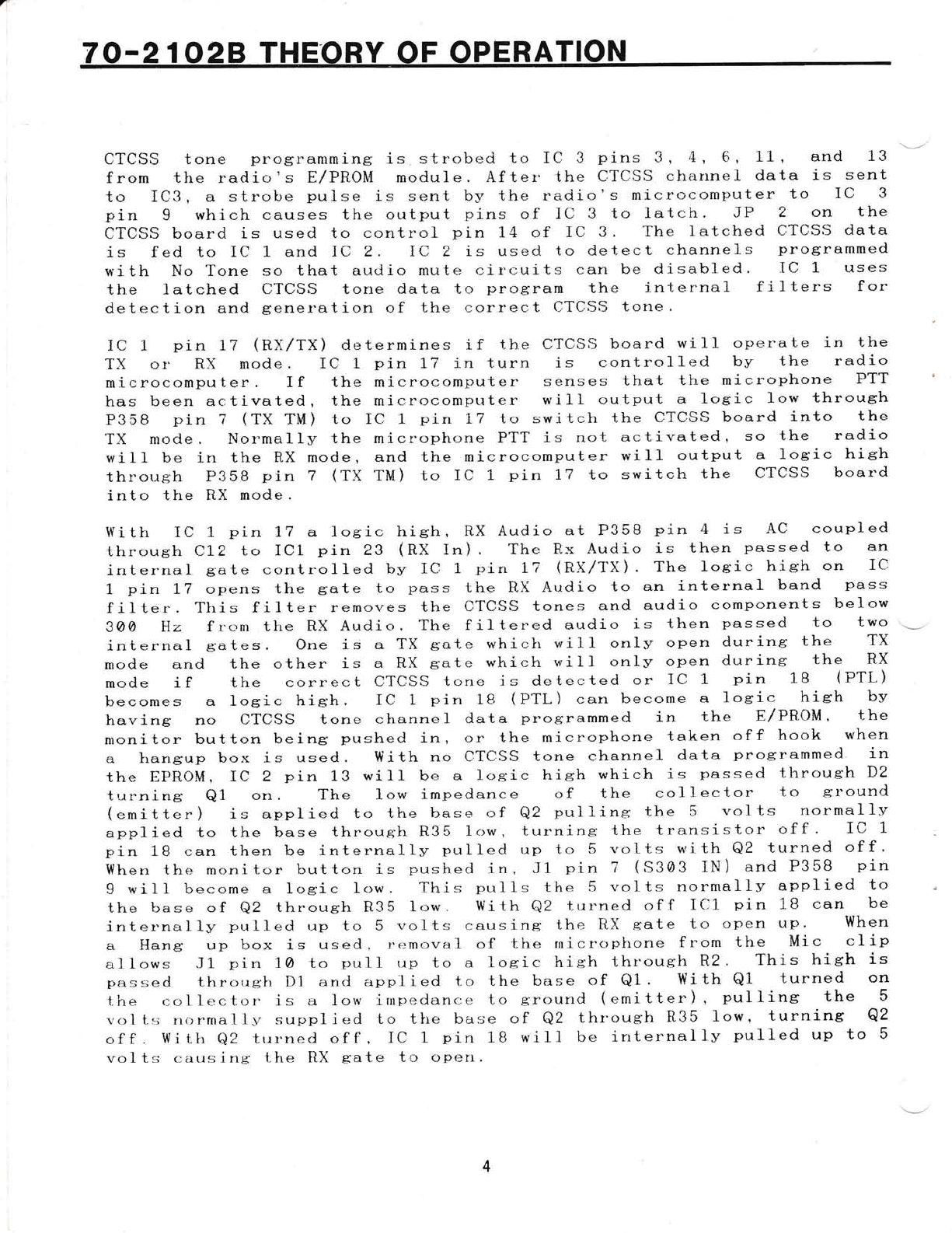
7O.21O28 THEORY OF OPERATION
CTCSS tone programming is. strobed to IC 3 pins 3, 4' 6, 11, and 13
from the radio's E/PROM module. After the CTCSS charrnel data is sent
to ICS, a strobe pulse is sent hy the radio's microcomputer to IC 3
pirr I which causes the output pins of IC 3 to latch. JP 2 on the
CTCSS board is used to contr"ol pin 1-4 of IC 3, The latched CTCSS data
is fed to IC 1 and IC 2. iC 2 is used to detect channeis proelrammed
wi th No Tone so that aurlio mute cir,;uits can tre disabled ' IC 1 uses
the latched CTCSS tone data to program the interrtal filters for
detection and generation of the correct CTCSS tone,
IC L pin 1? (nX/fX) determines if the CTCSS board will operate in the
TX (rr RX mode . IC l- pin L7 in turn i s control led by the radio
microcomputer. If the microcomput.er senses that the microphone PTT
has been activeted, the microcomputer will output a loeic low through
P35B pin ? (TX TM) to IC 1 pin L7 to switch the CTCSS board into the
TX nrode. Nor"maIly the microphone PTT is not activated, so the radio
will be in the RX moden and the microcomputer wiIl output a logic hish
throush P35B pin 7 (TX TM) to iC L pin L7 to switch the CTCSS board
into the RX mode.
\{ith ic l_ pin 17 a losic hish, RX Audio at P35B pin 4 is AC coupled
throueh C12 to IC1 pin 2g (nX In). The Ex Audio is then passed to an
internal sate controlled by IC 1 pil L7 (BX/TX). The losic hieh on IC
1 pin 17 opens the elate to pass the RX Audio to an internal band pass
filter. This filter remo\res the CTCSS tones and audio components below
300 Hz from the RX Audio. The filtered audio is then passed to two
internal g;ates . One is a TX E;ate which wi 11 only open during the TX
mode and the other is a RX eate which will only open during the RX
mode if the correct CTCSS tone is detected or IC l- pin 18 (PTL)
becomes a loeic high. IC 1 pin 18 (pU) can become a loeic hish bv
havins no CTCSS tone channel data prosrammed in the E/PBOM, the
monitor button being pushed in, er the microphone taken off hook when
a lrangup box is used. Uith no CTCSS tone channel data programmed. in
the EPROM, IC 2 pin 13 will be a loeic hish which is passed throueh D2
turninel Q1 on. The low impedance of the co1 lector to ground
( emi t ter ) is appl ied to the base c-f Q2 pul l ins the 5 vol ts normal lv
appl ied to the base throug'ir 835 1ow, turning the transistor of f ' IC 1
pin 18 can then be internally pulled up to 5 volts with Q2 turned off'
l{hen the monitor button is pushed in, J1 pin 7 (S303 iN) and P358 pin
I will become a logic Iow. This pu1ls the 5 volts normally applied to
the base of Q2 throush R35 1ow. With Q2 turned off IC1 pin 18 can be
internally pulled up to 5 volts causing the RX gate to open up' \{hen
a Hang up box is used, r6)mova1 of the rnicrophone f rom the Mic cl ip
allows J1 pin I@ to pull up to a losic hish throueh R2. This hish is
passed throush Dl and applied to the base of Ql. i{ith Q1 turned on
the collector is a 1ow impedance to g'round (emitter), pullins the 5
volts normally supplied to the base of Q2 throush R35 Iow, turnincl QZ
of f . \{i t}r Q2 tur-ned of f , IC 1 pin 18 will be internally pulled up to 5
vol ts caus ing t-he RX g-ate to open '

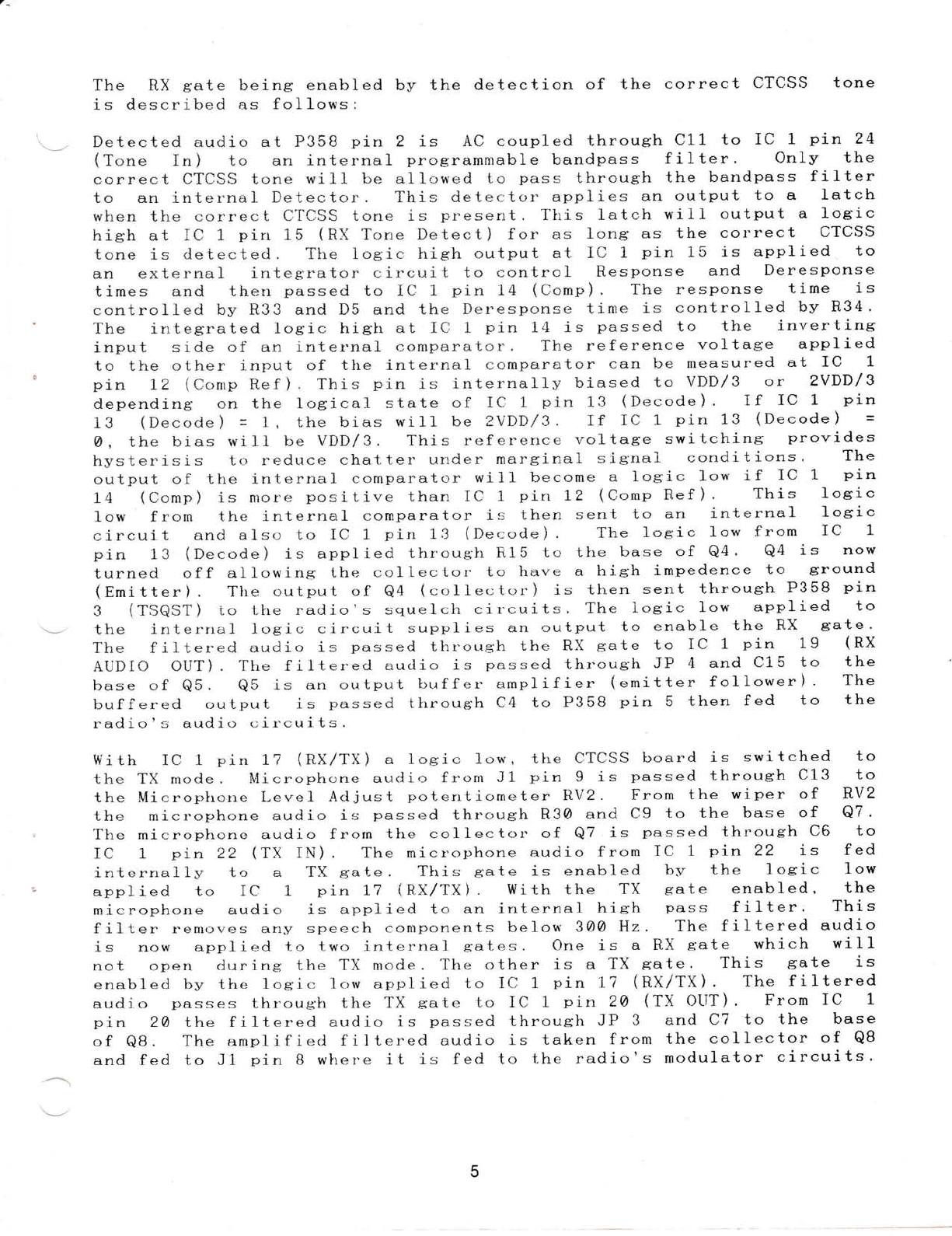
The RX eate beins enabled by the detection of the correct CTCSS tone
is descrikred as f ol1ows:
Detected audio at P35B pin 2 is AC coupled throuelh Cl-l to IC l pin 24
(Tone In) to an internal pro*;ramnable bandpass filter ' Onlv the
correct CTCSS tone will be allowed to pass through the bandpass filter
to an internal Detector. This detector applies an output to a l-atch
when the correct CTCSS tone is present, Tiris latch will output a loslc
hieh at IC l- pin 15 (RX Tone Detect) for as lone; as the correct CTCSS
tone is tle tected. The loeic hielh output at IC i pin 15 is applied to
an external inteErrator circuit to control Response and Deresponse
tj-mes and then passed to IC 1 pin 14 (Comp)' The response time is
controlled by R33 and D5 and the Deresponse time is controlled hv R34'
The integrated loeic hieh at IC 1 pin 14 is passed to the invertins
input side of an inter.nal comparator'. The ref erence voltage applied
to the other input of the internal comparator can be measured at IC 1
pin 72 (Comp Hef), This pin is internally biased to VDD/S or 2VDD/3
dependine on the logical state of IC 1 pin 13 (Decode). If IC I' pin
13 (Decode) = L, the bies will be 2VDD/3. If IC l- pin 13 (Decode) =
0, the bias wj-11 be VDD/3. This ref er"ence \roltase switching provides
hysterisis to reduce chatter under marginai signal conditions.
output of the inter6al comparator will become a. logic 1ow if IC 1The
pin
L4 (Comp) is 60re positive than IC 1 pitr 12 (Comn Bef) ' This losic
1ow from the i.nternal cornparator is then sent to an internal logic
circuit and als,: to IC 1 pin 13 (Decode ) . The losic low f rom IC 1
pin 13 (Decode) is applied throush R15 to the base of Q4' Q4 is now
turned of f al lowine lhe t:o1lector to have a hish impedence to €;round
{gm1tter). T}re output of Q4 (collector) is tLien sent through P35B pin
3 (TSQST) to the radio's squelch circuits. The losic 1ow applied to
the internal losic circuit supplies an output to enable the RX 8;ate'
The filtered audio is passecl through the RX sate to iC l pin 19 (nX
AUDIO OUT). Ttre f ilter.ecl auclio is passed through JP 4 and C15 to the
trase af Q5. Q5 is an outpgt buffer amplifier (emitter fotlower). The
buffered output is passed throush C4 to P35B pin 5 then fed to the
radio's audi o circui ts.
With 1C 1 pin 1.7 (RXITX) a loeic low, ttr,e CTCSS board is switched to
the TX mode. Microphone aurdio f rom J1 pin I is passed throush Cl-3 to
the Mir:ropfuo11e Level Acl just potentiometer RV2. From the wiper of R\r2
the microphone audio is passed thr'oush R30 and Cg to the base of Q7.
Tire microphone audio from the collector of Q7 is passed through C6 to
IC 1 pin 2? (tX IN). The microphone audio from IC 1 pin 22 is fed
internally to a TX sate ' This g'ate is enabled l>I' the losic 1ow
applied to IC 1 pin 1"7 (RX/TX). With the TX sate enabled, the
microphone audio is applied to an internal hish pass filter. This
f ilter removes^ any speech components below 3@O Hz. The f iltered audio
is now applir:d to two internal gates. One is a RX gate which will
not open durin€i the TX mode. The other is a TX gate' This gate is
enabled b), the loeic 1c,w applied tr: IC 1 pin 1.7 (RX/TX). The f iltered
audio passes throush the TX sate to IC 1 pin 20 (TX OfiT)' From IC 1
pin 20 the filtered arrdio is passed through JP 3 and C7 to the base
of QB. The amplifierl filtered audio is taken from the collector of QB
and fed to J1 pin B where it is fed to t-he radio's modulator circuits'

The losic 1ow applied to IC l pin L7 (itX/TX) also turns on an
internal audio generator. The frequency of the generator is
controlled b], the TX CTCSS data channel programming;. The CTCSS TX
tone is output at IC1 pin 16 (TONE OtlT). The TX CTCES tone j,s fed to
the CTCSS LE\iEL potentiometer RV1 which controls the amplitude of the
TX CTCSS tone. From the iciper of RV1 the llx CTCSS tone is f ed to a
De-emphasis circuit consisting of R16, C2, C3, and Rl. From R1 the
De-emphasizecl CTCSS tones are sent through P358 pin 6 to the Radio's
modulator circui-iry. It is necessary to feed ihe TX CTCSS tones
through tr De-emphasis network before the radio modulator circuitry
because the nrodulator contains a 6 dir per octave Pre-emphasis network '
This results in the CTCSS t<-rnes being transmitted f 1at ' The CTCgg
tones have to be transmitted flat since the CTCSS tones are detected
and filtered frour the RX audio before the De-emphasis network in the
audio PA section of a receiver.
|TCSS tone prosrammins. i s stroberf to IC 3 pins 3, 4, 6, l-1, and 13
from the radio's E/PROM module. After the CTCSS channel data is sent
to IC 3, a strobe pulse is seni by the radio's microcomputer to IC 3
pin I which causes the output pins of iC 3 to letch. JP 2 on the
CTCSS board is used to control pin 74 of IC 3. The letched CTCSS data
is fed to IC 1 and IC 2. IC 2 is used to detect channels proeirammed
with No Tone so that audio mute circuits csn be disabled' ILr 1 uses
the latched CTCSS tone data to pro€iram the internal filters for
deter;tion and €ieneration of the correct CTCSS tone, IC 4 is used to
process TX and RX audio.
IC t pin 17 (RX/TX) and IC 4 pin 5 (RX/TX) determines if the board
wi 11 operete in the TX or RX mode . IC l- pin 1-7 and IC 4 pin 5 in turn
are controlled try the radio microcomputer. If the microcomputer senses
that the microphorre PTT has been activated, the microcomputer will
output a 1oa'ic 1ow throush P3SB pin 7 (TX TM) to IC l pin L7 and IC &
pin 5 to sw j- l-ch the board into the TX mode. NormaIly the microphone
PTT is not activated, so the radio will be in the RX mode, and the
microcomputer wiII outpul a losic hish through P35B pin 7 (TX TM) to
IC L pin L7 ancl iC 4 pin 5 to switch the board into the RX mode.
Wi th IC 1 pin 17 an<l IC 4 pin 5 a loeic hish, Detected audio at P35B
pin 2 is AC coupled thror-reh c11 to IC l pin 24 (Tone In) to an
internal programmable bandpess filter. Only the correct CTCSS tone
will be allowed to pass through the bandpass filter to an internal
detector'. This detector applies an output to a latch when the correct
CTCSS tone is present. This latch will output a loeic hish et IC l-
pin 15 (RX Tgne Detect) for as long as the correct CTCSS tone is
detected. The losic }ish output at IC l- pin 15 is appl iecl to an
externql integrator circuit to control Response and Deresponse times
and then passed to IC 1 pirr 14 (Comp). The Response time is

oontrolled k,r. R33 and DS and the Deresponse time is controlled bv R34.
The intesrated loeic high at IC 1 pin 14 is passed to the inverting
input side of an internal comparator. The reference Yoltage applied
to the other input of the internal comparator can be measured at IC 1-
pin l2 (Comp Ref ) . This pin is internal1v biased to VDD/3 or 2VDD/3
depencling on the losical state of IC 1 pin 13 (Decode) ' If IC 1 pin
13 (Decode) = 1, the bias will be 2VDD/3. if IC 1 pin 13 (Decode) = O,
the bias witl be VDD/3. This reference voltase switching provides
hysterisis to reduce chatter uncler mar€iina1 signal condiiions ' The
output of the internal comparator will became a logic low if IC 1 pin
l4 (Comp) j.s more positive tiran 1C I pin i2 (Comp Ref ) . This logic
1ow is then sent to IC 1 pin 13 (Decode). The losic low from IC l- pin
,IQ ls fed two ways, to R15 and to D4. The losic iow fed to R15 is
applied to the base of Q4. 84 is nor,rr ''turned off allowing the
collector to har.e a hieh impedance to ground (Emitter) ' The output of
Q4 (collector) i= then sent thrqush P35B Fin 3 (TSQST) to the radio's
squelch circuits. The iogic low f e,l to D4 pulls the 5 volts supplied
through R2? to a 1ow which is passed to IC 4 pin 6 (RX Audio Enable) '
The loSic low on IC 4 pin 6 is used to enai:, 1e internal audio E;ates for
RX audi-o processinE;.
RX audio at P35B pin zl is AC coupled throush C12 to IC 4 pin 11 {nX
iN) which is fe<i to an internal audio g;ate controlled b'y IC 4 pin 5
(RX / TX). The losic his'h orr IC 4 pin 5 opens the €;ate to pass the RX
audio to ari intely1al Lrapdpass f i. 1.i;er. This f ilter removes the CTCSS
tc;nes and Audio compolenLs below 300 Hz f rom the Rx audio. The
filter-ecl Audio carl then be sent one of two wajrs depending on the 1og'ic
status of IC 4 pin 7 (Privac5' Enable ) '
f IC 4 pin ? is a 1r:54i-c 1ow, the f iltered audio is f ed to IC 4 pin 1
.\
.bltter r:u'tl tfien external],y AC cou.pled through C16 to IC 4 pin 24
Balancecl L{ojulator ) . The ha1an,:ed modulator is enab}ed bv a 3333 Hz
carrier oI' disabled
status of IC { pin
3333 Hz carr"ier to the
RX audio appl ied to
inverted audio from ihe
output bandpass f ilter.
and adds 4 db of elain to
of the bandpass f i lter
by a DC potential applied to it depending on the
7 (Pri Enable). The low on IC 4 pin 7 applies a
baianced modul,ator which frequency inverts the
it f rr:rn IC 4 pin 24 (BMOD). The frequencY
balanced modulator is then fed to an internal
The bandpass filter removes any clock noise
the inverted and fi1tered audio' The output
is feci to a RX audio Elate which is enabled bv
the losic lorv ot1 IC 4 pin 6 (RX Audio Enable)
filtered audio is rlo$' output on IC 4 pin L4 (nX . The inr.erted and
Out).
If IC 4 pin 7 (Privacy Enable) is a losic high, a DC potential is
appliecl t,-, the traltrncecl no<iulertor cilsabling it and the filtered audio
is routed around lire balanced rnodulator and output bandpass filter
to a RX aucii6: geite. This RX Eiate is enabled by the logic 1ow on IC 4
pin 6 (RX Auclio Enable). 'Ihe f ilterecl rron-inr.erted audio is now output
on IC ,1 pin 14 (RX Or-rt).
From IC ;l pin 1,1 (RX Ourt ) the processed audio is AC coupled through
Cl5 to the base af Q5. Q5 is if,rr output buffer amplifier (emitter
follower) The buffered orrtprrt j.s AC coupled throush C4 to P35B pin 5
(nX Out ) Lhen f e,d to the radio's aud.i o cir-cuits '
7

In the RX starrdby mode where iC 4 pin 6 (RX Audio Enable) - L, the RX
auciio gate rri1l he turned off trut can be enabled by a logic hish on iC
ul pin 3 (PTL). IC 4 pin 3 can become a losic hisir by iravint the
moni l-c-r srgitch pushed in or k,y taking the microphone of f hook when a
hangup bo,t is used. \f hen ttre morri tor h,utton is pushed in, J1 pin i
(SS03 IN) and P35B pin I (MON) rvil1 bec:ome a loeic 1ow. This pul1s the
5 r.olts normaliy app,lied to the base of Q2 throush F,35 1ow. With Q2
turned ,:f f IC 4 pin 3 can be internelly puIled up to 5 volts causing
the RX Audio gate to open up. Hhen a Hang up box is used, removal of
the microphone f rom the Mic cl ip al1ows J1 pin LO t.o putl up tt> a
losic hish thr"ough R2. f'his hish is passed through D1 and R37 and
applied to the bese of Qi, With Qi turned on the collector ls a low
impedance to ground (emi,tter), pullins the 5 v<:1is norma115. supplied
to the trase of Q2 throush R35 low, turnins Q2 off. With Q2 turned
off, IC 4 pin 3 (PTL) will be internally puiled up to 5 volts causing
the RX e'ate to open. IC 4 pin 7 (Privacy Enab1e) has no effect on the
Rx audio as lons'as IC 4 pin 6 (nX Audio Enable) is a loe'ic hieh.
If Notone is programmeci in the radio E/PROM, iC 2 orrtputs a losic hieh
on pin 13 . Thi s irigh f rom pin 13 is f ed to R2B and I)3 . The losi c hish
applied to RzB is fed to the base of QG turnins it on. This causes
the collector to have a Low impedance to ground (emitter) which pulIs
the 5 r.,olts normelly supplied to IC 4 pin 6 (RX Audio Enable) through
R27 lt,w, enabl ing the RX audio .gate to opell . The logic hish f ed to
D3 is passed to IC 4 pin ? {Prir.acy Enab}e ) turning the internal
balanced modulator off. In tiris way the Audio is unmuted and Non-
Inverted.
1{ith IC i pirr 17 (RX/TX) and iC 4 pin 5 (RX/TX) a loeir:1ow, the board
is swi tched into the TX mode. Microphone audio from Jl pin I is
passed through CL3 to the tr{icrophone 1er.e1 adjust potentiometer RV2.
From the wiper of RVz the microphone auciio is passed throueh R30 and
Cg to tkre base of Q7. The rnicrophone audio f rom the collector of QT
is y:assed throush CG t,r IC 4 pin 1,3 (fX in). The microphone audio
f rom IC 4 pin l-3 is f ed internally to a TX sate, This sate is enabled
by the loeic low applied to IC 4 pin 5 (RX/TX). \{ith the TX sate
enai>1ed, the rnicrophone aud j.o is appl ied to an internai bancipass
f ilter, 'Ihe berndpass f i l ter removes any speech component.s below 300
Hz. The f il tered mic, rophc,ne audio can no\{ be sent two w&3r5 depending
on the logic statrrs c-f IC ztr pin 7 (Privacy Enable).
If 1C 4 pin 7 is a 1c,gic 1ow, the filtered microphone audio is fed to
IC 4 pin 1 (Fiiter Out) then externa113. ng coupled through CL6 to IC 4
pin 24 (P,a1an,:ed Modulator). The balanced modulator is enabled by a
3333 Hz carrier er" disabled by a DC potential applieci to it depending
on the status of ICI 4 pin 7 (Pri En). The 1ow on IC 4 pin 7 applies a
3333 Hz. cat't'ir:r t,-, tlre balanced modulator which frequency inverts the
filtered microphone auclio applied to it from 1C 4 pin 24 (BMOD). The
fr"equency inverted microphone audio frr-rm the balanced modulator is
then fed to errl jrrternal or;tput lrandpas;s filter. T']re bandpass filter'
removes i-rny c,Lock nc,i.l;e ernd adcis ;1 citl of Eiain to the inverted and
filtr,rred microphone audio. Tire output ,-,f the bandpass filter is fed

to a TX gatr, t,iricir j.s enabled by the iosii-. 1c,w c,n iC 4 pin 5 (RX/TX)
The inwerteci and f i ltered auc{ic; i: now output on IC 4 pin 15 (TX Out)
If Itl 4 r:in ? (Friyac5' Enat'}e) is a 1c'gi': higir, a DC potential is
applieci .bo the I:alan<;ed mociulator di sablins it and the f iltereci
mi crop6cne ar-rciio i s routed arounC ihe Lralanceci modulator and output
bandpa*.s f itie:' to a TX Sate. This gate is enabled bv the logic low
on IC 4 pil 5 (RX/TX). The rrorr-inverted f iltereci audio is now output
on IC,i pin i5 (TX Ot.rt).
Fpom iC 4 pj.n j 5 the processed microphone audio is passeci through CT
to the trase gf QB. The ampl ified fi ltered microphone audio is taken
from the collector of QS an{ fed to J1 pin B w}repe it is feci to the
radio's modulator circuits '
The losic 1.;w applied io IC i. pin i7 iRf/TX) tprns on an internal
ar-rciio Eienerator'. The f 1-E:q.uency of the Ejeneratgr' is cr:ntrol1ed by the
TX CTCSS data ,:trannel programmin.q'. The CTCSS TX tone is output at TC
1 pin 16 (Tone Out ). 'Ihe: TX CTCSS ion.: is f ed t,: the CTCSS LEVEL
potent-iomet+r RV1 which .:otttrols the amplitr-rde of tl:e TX CTCSS tone '
Fr.om the wiper of R\r1 the TX CTCSS|one is fed to a De-emphasis
circuit cLrnsisiirrg of R16, C2, C3, and Ri. From R1 the De-emphasized
CTCSS tanes are sent through P35g pin 6 to the Radio's modulator
circuitrv' It is necessarlr to feed the TX CTCSS tanes through a De-
emphasis networ-k k,efor.e the radio rrrodulator circuitry because the
moilul,ator. corltains a 6 db Iler octar.e Pre-enrphasis network' This
r.esults in the CTCSS tones beins tr-ernsmitted f 1at ' The CTCSS tones
have to be transmitted flat since tire CTCSS tones are detected and
filter.ed- fr.-:m lhe RX audio before the De-emphasis network in the audio
PA sectic,n of a receir"er'.
When Notone is progr"ammed in the raciio
frish f r':m pin 13. This losic hish is
Q3. With Q3 turned on, the cc, liector
(emitter) and applies this to the iurn';t
E/PROM, IC 2 outPuts a logic
f ed through Rl ? to the base Lrf
has a 1ow impedance to ground
ion of R16 and C3 '
I

z.
3.
4.
5.
7O-?1028 CTCSS ENCODER/DECODER
7O-21O2-7 CTCSS WITH PRIVATE SOUELCH KIT
INSTALLATION INSTRUC? IONS
SYNTECH-I UNDER*DASH AND TRUNK-UOUNT I{ODELS ONLY
1. Remove the 4 screws securing the radio top and bottom covers and
remove the eovers.
Turn the radio upside-down on the bench. Seresr the threaded
standoff supplied with the CTCSS board into the right hand hole
Iocated in the option area in front of the reeeiver board.
If the 7A-2L95 microphone hangup box is to be install-ed, the jumper
JPI must be removed from the CTCSS board for proper moni-tor
operat ion.
As supplied, the CTCSS board can be programmed to encode and decode
on any of the standard EIA GrouB A and B tones from VL.g to 24L.8
Hz. It Group C Eones are desired, remove JPZ from the CTCSS board.
Refer to CTCSS Modif ied programming paqes if siruultaneous A/C, B/C
or A/B/C groups programming is required.
Remove the jumper plug from J358 (right. side of receiver board) and
eonnect the B pin conneetor and cable running from P358 on the
CTCSS board-
Connect Ehe 8 pin plug nith the singte wire , P357, to J357 on the
receiver board.
Remove the clear sleeve and jumper plug from the floating option
eonnector PI. Connect Pl to JI on the CTCSS board-
Eeed the remaining I pin connecLor and cable eonnected to P9O3
(CTCSS Board) to the top of t.he radio through t.he opening just
behind the front panel assembly. Remove the E/PROU module and
connect P9O3 to the J9O3 jack on the E/PROM modu1e. Reinstall the
E/PROI,I module.
9. Carefully position the CTCSS board over the option area, connector
side down and install the 3 serews supplied (left side and center)
to secure the board in pIace.
10. CTCSS modulat.ion ad justment
back of the PCB. is made by RvI, accessible from the
11. tilic leveI adjustment is factory set for standard microphone.
5.
7.
8.
10

the
the
1. Remove
remove
7O-21O28 CTCSS ENCODER/DECODER
7O-2102-7 CTCSS WITH PRIVATE SOUETCH KIT
INSTALLATION INSTRUCTIONS
(70-336 and 70-326 only)
4 screws securing the radio top
covers. and bottom covers and
the C?CSS board into
area at the front of
2. $crew the threaded standoff supplied with
the right hand hole located in the option
the radio.
5.
-{t.
3.
4.
7-
8.
9.
rf the 7o-?195 microphone hangup box is to be instarred, the
jumper JPr must be removed from the crcss board for proper
monitor operation.
As supplied, the crcss board can be programmed to encode and
decode on any of the standard ErA Group A and B tones from 7L.g
to 24L.8 Hz. If only Group C tones are desired, remove JP2 from
the CTCS$ board. Refer to the CTCSS Modified Tone prograuming
pages for simultaneous A/C, ts/C or A/B/C groups programming.
connect t.he I pin connector and cable running from p35g on the
CTCSS board to the JZOZ jack on the radio main pCB.
Conneet t.he I pin plug with the single wire, pt!7, to JZOS on
Ehe radio main PcB. Remove the jumper Jpzor, roeaLed on the top
of Ehe radio main board between JZOZ and J9OI.
Connect PI and (the 13 pin floating option connector running
from J9O4 on the radio main PCB) to JI on the CTCSS board.
Connect the remaining 8 pin eonnector running from P9O3 on the
CTCSS board to J9O1 on the radio main pCB.
carefurry position the crcss board over the option area,
connector side down and install the 3 screws supplied (Ieft side
and center) to secure the board in place.
CTCSS modulation adjustment is made by RVI, accessible from the
back of the GTCSS board.
Mic leveI adjustment is factory set for the Standard mic.
10.
11.
11

PRIVATE SQUELCH PROGRAMMING INSTRUCTIONS
USING THE 7A_2L02_? CTCSS ENCODER/DECODER WITH PRIVATE SQUELCH
The 7q-ZL@?-? scrembler function can be controlled in two ways
1. CTCSS tone programming controlling the operation of the scrambler
function.
2, Direct Private/Cl-ear control of the scrambler by using: one of the
front panel switches normally used for scan control.
PRIVATE/CLEAR CONTROL METHOD +1
In the first method, JPA and/or JPB are used to connect IC 4 pin 7
(Privacy Enable) to data lines DO-DS (t*o rows labeled PRIV SEL 0-5 on
the PCB as shown below) , which program CTCSS tone data into IC 1 ' JPA
and JPB must eech be connected to no more than one CTCSS data line.
Clear operation (no scrambline./descramblins) will occur on all tone
programmed trensmit/receive channels where losic HIGH data lines (PRIV
SEL points) 0-5 are connected to JPA or JPB, oI" if CTCSS is disabled
by programming; No Tone. Scrambling/descramblins will occur on tone
programmed transmi t./receive channels where all PRMEL points 0-5
which are connected to JPA or JPB are losic LOI{.
EXAMPLE 1: From the CTCSS Tone Programming Truth Table, find column
D3. Note that all- of the CTCSS tones from 67.0 Hz to 141-.3 Hz use a
losic hish, and that al l of the CTCSS tones f rom 146. 2 Hz to 24'1. .B Hz
use a losic low, Soldering a wire link jumper betn,een JPA end PRIV SEL
3 would resuft in all tones from 67,0 Hz to 14L.3 Hz kreing marked as
CIear (unscrambled), and aI1 tones from L46.2 Hz to 241'.8 Hz being
marked as Private (scrambled).
EXAMPLE 2: Jumpers installed between JPA and PBIV SEL 3 and also
between JPB and PRIV SEL 2. This would result in all tones from 67.@
Hz to 186.2 Hz beins marked as Clear and all tones from 192.8 Hz to
24t.8 Hz beins marked es Private. As the example indicates, when both
JPA and JPB are used, a logic hish will override a loeic 1ow.
IMPORTANT NOTE
If JPA and JPB are not connected to any of the six data lines, then
all radio channels that are proelrammed with CTCSS tones will be
scrambled. Also note that the cor"respondins PRIV SEL points 0-5 in the
two rows are connected together, allowing'JPA and JPB to be connected
to either row.
PRIV gEL
A6432lO
q€.€, o o o
@Joooooo
PRIV 8EL
A 5 43 210
EL3-Yooo
trf6h o o
B
12
EXATPLE IEXAMPLE 2

7O-21O2-7 PRIVATE/CLEAR SWITCH OPTION
PRIVATE/CLEAR CONTROL METHOD #2
1n the seconci method, the scrami:linc operatir-rn is not conLr-o11ed by
CTCSS progranrming br-rt by a f ront panel FrivaterrCf ear switch, howev,lr,
tlre boarC is sii11 CTCSS tc,ne depr:ndent. See tire Prir.ate/Cl ear Switch
Oprion Furrct j-on Terble beiow.
PRIVATE/CLEAR S1!'ITCH OPTION FTI}JCTiTJN TABLE
MON PRIV/CLEAR CT{--SS TONE IS:
R:{/TX IN/OiJT iN/OLTT'- PRCGRAI{T{ED/DECODED RX AT]DIO TX AT]DIQ
STANDBY RX
h,ioDE Rli OL]'I
rNi YES /NO OFF OFF
XyE$*_____/_lo CLEAR oFF
D\'
x.{oDE RX
RX
tt\
X
XY
ULt
Ili
l\ (-)
YES / ti/A
/ i'Es
l\,/ A
N/A
N/A
CLEAR
t,I,F,AH OFF
OFF
l_E$___ _ -1___1:E,l_ SCRAMBLED OFF
TX
.\{.-)Dtr
NOTES:
TX
'r\'
'T-V
li/A
NiA X
()[i t
TAI
NO
YES
YES
OFF
OFF
OFF
i-.LEAR
CLEAR
SCRAMBLED
Switch posi tion ntakes no dif f erence
= Nt,: t Appi i cal-;i e ,
The standb3'mode is when the RX audio is muteci trecar.tse the board has
not decode<i the,:or"rect CTCSS tone that is programmed in the radio
E/PROM. llhen ltre MONiTOR switch is pushed'*-ut, tlie RX audit, r'emains
muted. i{hen the I,IONITOR swi tch is plrshed in, the RX audio is turned
or1 and ttre status of the PRiVATE/CLEAB swi tch has no control on the
ciear audi<-r.
1n the tlX mode, wherr ttrere is no CT'CSS tone prog,rammed in the radio
E/PIf(JM, tire RX arrriio is r:nmuteci. Tire MONITOR and the PRIVATE/CLEAR
swi tches have no ef f e,:t. on tlre clear RX audio. \{'hen there is a CTCSS
Lone pr-ogr.trnilneci in the raCio E/PF.OM anci the board detects and decodes
tirert CTCSS tr>rie, tire strrtus .-:f the PRMTE/CI.EAR switch will control
Lhe R\ aucli<>. 1F the PFtiVATE/CLEAR snitch is pirshed out. the RX audio
wiil be c1ear., iF tlr.e PRiVATE/CLEAR swj.tch is pushed in, the RX audio
will be s.;r'anrtrled.
Tire board is pul inLo the TX m,:de rvh.er: tiie radio microphone PTT is
enab l eci .i f there is n.-, CTCSS bt)n<', prr-.,g;ramnr,':d in the radio E/PROM '
the status of the PIIIVA'I'E/CLEAil swi tch ]ra:; no ef f ect on the TX eudic, '
If iherc is a CTCSI-l t,;ne prosr.ammecl irr the r"aciio E/PROM, the statr-rs of
iire PRI\riil'E/C1-tlAit swi tch wi.[ I ,:,,.,ntro1 thr: TX audio. If the
PLIIVA'IE,/CI,EAI1 switch is push.-:ci orit, the TX erudit: rtil1 be clear' If
the PitiVATE/CLEAii r;witc'h j.s l;r-rslr,:d irr, th,: TX audio rvi11 be scrambled.
13

7O.21O2-7 PRIVATE/CLEAR SWITCH OPTION
If the Priority button is to
remove R10, R26, and RzB from
from the component side of
conponent side of the board as
if installed.
PRIVATE/CLEAH CONTROL METHOD #2
be used f or the Prir.ate/C1ear" switch,
the solder slde of the board. Remove D3
the t>oard. Add a jumper wire on the
in the Fisure below. Remove JPA and JPE
Add Jumper
Remove D3
PRI BUTTON AS PRIVATE/CLEAB SWITCH
il- #? #lh w -q *i
Iffi.'.\/"ffi
v sas****o, * '(_.trmt-t:.r* *+,.ili-jlMr'++++.'+d\q
2 o$ Irc ff \-*;i&'1.*,*" .*, ;;.; ; il-+ . pJ{;Fa.
.."...r 6e2l
lnrtr
"t'ft \srerr I
Bemove R2B
Remove R26
R10
3 f-eeffi]
: 4-- *"tuFls ',f",f Jx
'*/.*,{!ig,re€4@
14

V O/ 21O2.7 PRIVATE/CLEAR SWITCH OPTION
i f iiie Scari irut lon is Lo f:'=
Ri1, F26, atrci R.28 from the
the comp+nent side r-rf tire
s i-de of the br:ar-d err irr
installed.
PRIVATE/CLEAR CONTROL METHOD #2
used for tire Prir.ate,/C1ear swi.tch, remo\ie
sc, lder side of the bcard. Remove D3 f t'out
board . Add a jumpe.r wi re orr lhe component
t ire f i gure be 1ow . Remove JPA end JPB i f
Add Jumper
Remove D3
SCAN BUTTON AS PRIVATE/CLEAR SWITCH
&*-e#H&
-G #s##Hs*##&
4 u*€\.d\ntqr ffi +\*fift:Ildrry
g? ffi ffi ii !*'ied;*-*-"**.';;;;l;-{'-Fffi"
ffi$ *r.#
-r h'o
l:1 t:i ;::;;:l ii i
Ill!!1i:i:;::;t i
; ,EES 5
'i,.,tfi ;, E '"..
HiiE'fu;
. , F"
:n ,fiil
-, :" t::, -:::.l. ..::,il,i " ..I
. iil ,i ,iro,
F.g=
l[El, Remove R11
ffiffiiHBHffitr
ill -oeos' 'Sor{
iii:1 lC+ d N r' d: d.d
;tt c G ( 6@
i:1 1: , :"" .
-'r,tl ",g5fle l
L.,i" Itii.i
1.,t,. U- ,
E(EI Itr-.'- ' ii rHsEi
:::1;t:iitlli
tu
c1r,.'trB:.
cb
U
lfr "'p ,[ L
Fas ll tl
f'lll inr. H H
il[
:tub:& o Al
,d E
Flemove R28
Remove R26
15

TONE PROGRAMMING TRUTH TABLE
TONE TONE
FREQUENCY GROUP M D1 D2 D3 D4 D5 NOTE: D5. is not E/PROM
prog'ra.mmable but is
controlled by JPz.
NOTE:57 Hz cannot be used
with mode 1 programmable
CTCSS scrambler operation
since DO-DS are all logic
hiqrhs.
i. 11111
1111L0/
@111L1
1111Ae,
\@1111
@1L11E,
@@'1 111
@11LgA
11@111
1011lE
@L@111
LAi. 1A@
@@L1L@
@a11@@
11011g
11@10@
@L@11@
@187@@
10@11@
L@UL@@
@@@1r_@
@@@L@@
l_11@1@
111EOA
@1L@1@
@11@@@
1@1@LA
L@LA@@
@41@7@
@@100@
11@@L@
11@A@@
@t@@L@
@L@@@@
10@@L@
L@@A@@
@@@@1@
@@@@aa
C
B
C
A
C
B
C
A
c
B
C
A
B
A
B
A
B
A
B
A
B
A
B
A
B
A
B
A
B
A
B
A
B
A
B
A
B
57 .@ Hz
7t.9 Hz
74.4 Hz
77.@ Hz
79.7 Hz
82 .5 Hz
85.4 Hz
88.5 Hz
91.5 Hz
94.8 Hz
97 .4 Hz
1@@ .@ Hz
183.5 Hz
LA7 .2 Hz
114.8 Hz
118.8 Hz
L23.@ Hz
L27 .3 Hz
l-31 .8 Hz
136.5 Hz
141 .3 Hz
L46.2 Hz
151.4 Hz
155.7 Hz
162.2 Hz
167.9 Hz
173.8 Hz
L79.9 Hz
186.2 Hz
L92.8 Hz
203.5 Hz
zto .7 Hz
21.8 . 1 Hz
225.7 Hz
233.6 Hz
241 .8 Hz
No Tone
16

7 0-2 1 028/ 7 0-2 1 o^2-7 SCHEMATIC
R31
1K
JUMPER NOTES:
JP,' HANGEB SELECT
JP2 CTCSS RANGE SELECT
JP3 AND JP4 JUMPERS ARE
USED WHEN MXOO4 IS OMITIED.
I ourpur I
| "r.r." I
P358
MON
c8v
TXTM
TXTONE
AFOUT
AFIN
TSOST
CALL
UP
DN
HANGUP
MICIN
MtcouT
s3g3rN
PTTIN
PTTOU
s3g2 0 u
s302 rN
ssslou
s361 tN
PeoS
+5V
STB
DT6
DT1
DT2
oT3
DT4
GND
R33 1 s2075K
NOTES ;
'1. RESISTORS 1/4w.
2. ALL CAPACITANCE lN UF
MXO04P TXOUT
RXIN HIUU r
Rx,tTX PILDEC
HlI'ii6trtt PrLour
FHMfri MooE I
PrLrN lc4 MoDE 2
FiiEf FrrR
SEBDAT
SERCLK BMOO
LOAD/L-FTCF BIAS
PTL
xrAL rrrE
r, ".."rrtl \ 2sc458
ioK Ii s2o7sK
--N
R9,10,1 1 I ozv
=o oHMs Laroru*
PRrv^cY I lD6-',s rsioisr
SELECT I Lr e+----------1^--:ffi cD4o78B
tuFl louFl ro ALL
1 32075K
TXtN '"'--- TXOUT
RXIN RXOUT
TONEIN TONEOUT
tlr D-ECOTE
RXTONE DETECT
lc'l coMP
CMP BEF
BIA S
LOAD/Lf,TEfr
xrAL ITAL
17

7 0-21o^2r,/7 0-2102-7 PC BOARD
; i:ri r:
;s "n"
i': \/
;.rr""t{l
4
.€ \:) #aEHssH,## * U *u -rler "## S# +sH {r s,l* s{
H M ks66,*.***+r- L.," \_. i6ff,:::.,#-*
02 Crr4" rfiE S '.-fpd-.**-, -;;*:;i;;;;.*F{r... _ . __.","e1.S.e-,
#.sHs$fr,+#B*#
,ei
e+.4 s n. ?-::
70-2102E.170-2102-7 TOP VIEW
l3l c rp
ClB33
EEr3:4
E. 5.
ET
H...8
H'. il
sc
*:i::::: ar
7o-21028 B:rlotil :rEW
;ii'::':; . ,. , ,,'i;i''t:n::l'
'i::tidr ,rc {- 4- ; J ; " 3: :l r
r:: .1;+. g s s E'.E q eii ii .
-;,fifrHEEEF,.Ei;.i
1 1 ;;1;;i liii;r;! ii;i:
,lnd :'nio: ; :; l::::::,:::::
EH :]:
Lt g.' n.ii,
: :t., : ::
-
L..J
;.::i:.
:tsf ::;i i'ir
@:1
70-2102-7
' -'-'-'-'n fi3fr ii: iii ii:. ::: :
l-ra
r; ::i: iGrcit ;i,: :r.,r :r:'l
,1 , , '* -* ":. .;:"
, .:. cN.
.,...,.:...,...-..., -..1 : . .. -.,' :El
BOTTOM VIEW
l-1."*
Fas
f*l'nol
85
EE
E _=B
H'. H
n:: t:El
DESCRIPTION
CTCSS PCB Assembly
Threaded Standoff
3 x 6 mm Panhead Screw
CTCSS /PVT Squelch PCB
Threaded Standoff
3 x 6 nrn Panhead Screw
7O-21028 KIT COMPONENTS
QUANTITY
I
1
3
70-2102-7 KIT COMPONENTS
Assembly 1
1
3
PART NTIMBER
7 o-07 527 |
7 0-L56072
7 0- 151355
7 0-07 5272
70- 15 6072
70-15 1355
i;, .t .,;N'll"
a ,pv
i di'
i iii
li:; tir r:l:lu:r,:r rr: i:rL
t!' t) l
a1 ... .. t::!
.,.-
. +-a
ffit,
cii. tre;:::.
:H.
*fl
18

7 0-2102B/7 0-2 1 02-7 PARTS LIST
rc1
lC2
IC3
IC 4*
R15
010
Q6
r14
REF. LOC.
.r1 K2
P358 c2
P903 A2
DESCRIPTION
JACKS & PLUGS
PART NO.
70-1s9098
70-03406s
7 0-034066
7 0-07 6 3BB
7 o-07 6742-
70-076081
7 0-07 637 4
70-144045
7 0-144045
70-144033
7 0-144029
7 0-144032
7 0-744032
70-144001
70-144001
70-144019
7 A-74 4032
7 0-144032
7 0-144037
'7 0-144067
7 0-744029
7 0-14407 4
70-144018
7 0-144027
70-144014
70-144015
7 0-r44021
70-144031
7 0-744029
7 0-744029
7 0-144029
7 0-144029
7 0-744032
70-144003
70-144019
7 0-L44042
70-14s064
7 0-744069
7 0-r44029
7 0-144029
7 0-144034
7 0-144034
7 0-7440r9
REF. LOC.
cl 04
c2 L16
c3 L15
c4 cI1
C5 B7
c6* H8
c7* E7
CB* D9
C9* 15
c10* Jt1
CI1 G5
cl2 H5
c13* 13
c14 03
c15 E9
c16* ,117
cl1 u11
CI8 U13
C19 R1 B
c20 s17
D1 L7
D2 M7
D3* N7
D4* L14
D5 Q1B
D6* N5
D7* M6
x1 s12
PCB
Q1 t9
Q2 Ll1
Q3 N14
Q4 N1B
Q5 C10
Q6* M14
Q"7* 16
Q8* E9
*For Model
DE SCRIPTION
TANTALUM CAPACTTORS
RV 1 M17
RV 2* t4
Rl K15
R2 K5
Da A c ^l
^Jr=rJ V=
R617rB R4
R9,10 M3
R1I N3
R12 D10
R13 D10
R14 B10
\.15 017
R16 M16
R17 N13
Rl 8* E8
R19* E7
R2 0* D7
R21* DB
R22* J5
R23* 15
R24* D6
R25* D6
R26* L6
P'27* Kl3
R28* L13
R29 R4
R30* T4
R31 c1l
R32 T12
R33 Qt1
R34 R17
R35 J10
R36 L10
R37 L8
R3B M9
R39 MI7
10uf 16V
2.zLrf 76V
1Ouf 16v
1Ouf 16V
1uf 35V
1uf 35V
2.2uf l6v
2.2uf 76v
1uf 35V
luf 35V
CHIP CAPACITORS
.1uf
.1uf
470Opf
.1uf
.1uf
.1uf
33pf CH
33pf CH
.1uf
.1uf
D IODE S
TSzTf5x
132075K
152 075K
1s2 075K
1s2075K
152 075K
132 075K
MI SCELLANEOUS
1 MHz Crystal
PCB BIAnK
TRANSI STORS
PART NO.
70-138065
70-13805s
7 0-1 3B 065
70-138065
70-138087
70-138087
70-13B0ss
70-13805s
70-138087
70-138087
7 0-133047
7 0-133047
7 0-131247
70-133047
70-133047
7 0-133047
7 0-1 311 92
7 0-731192
7 0-733047
70-133047
70-085001
70-085001
70-08s001
70-085001
70-08s001
70-085001
70-085001
7 o-128024
7 0-07 0227
70-080082
70-080082
70-080082
70-080082
70-080082
70-080082
70-080082
70-080082
oack, 13 pin
9 wire cable W 2 plugs
B wire cable W 1 plug
INTEGRATED CIRCUITS
MX365 P Dip (Plastic)
I{D14 O 7 8BP
HD14174BP
Mx004P Dip (PIastic)
VARIABLE RESISTORS
Trimmer 10K
Trimmer 10K
CHIP RESISTORS
33K 1/8 w
10K 1/8 w
22K l//g Vt
22K 1/B w
zero ohm
zero ohm
1K 1/B w
22K t/B w
22K t/8 w
100K 1/8 vr
2.2K 7/8 w
10K 1/8 w
22 ohm 7/B w
820 ohm 7/8 w
6.8K 1,/B w
270 ohm l/B w
470 ohm 1/8 w
1.sK 1/8 }[
lsK 1/B w
10K 1/B w
10K 1/8 w
10K 1,/8 w
10K 1/8 w
22K 7/8 w
12 ohm l/8 w
lK 1/B w
1 MEc L/8 W
560K 1,/8 w
B2 0K 1,/8 W
1 0K 1,/B W
10K 1/8 w
4'lR l/B w
41K t/8 w
1K 1,/B W
2SC45B
2SC45B
2SC458
2SC45B
2SC458
2SC458
2sc458
2SC458
7 0-2102-7 only .
19

IFIED TONE PROGRAMMING
(FOR SYN-TECH-T, 7 O-336 AND 7O-526]
The 7O*2|OZB/2LO2-7 CTCSS board can be programmed for 3I EIA tones in
Group A and B. If JPZ is removed, 5 Group C Lones can be programmed, but
Group A and B tones are not programmable. To allow simultaneous
programming of Groups A and C, Groups B and C or Groups A, B and C tones,
follow the instruct.ions given below.
l. S_f mu_Ilageq.u-8"_G-E_qup_A and C Prosramminq
Remove JPZ and reposit.ion R29 as shown. Programming
as follows; A group tones can be proqrammed normaIly.
see chart below:
should then be
For C group
TOUL PROGRAIvIIIED
118.8
1IO. 9
103.5
94. B
82 .5
7L.9
ERqQUENCjT
97 .4 klz
91.5 Hz
85.4 Hz
79.7 Hz
7 4.4 Hz
67.O Hz
GROUP.
C
C
C
C
C
C
EXAMPLE: FoT a
be programmed.
B Group tones desired frequency of 97.4 Hz, the frequency of 118.8 must
are not proqrammable in this configuration.
RA fr1o
r{rr-
,r-T 'klt
MOVE R29 TO
r,l
83r'
.h3r:
r "El
{=:
cr? c1a flcrs
Brsu
Sns*
E5
nI
In
20
";.;."; 9
EEEEiAE A
frflHAflnn E
E3i-
, E! e::
;:,,*, :;: .
. [tr.;'i
' 'Ei'
:..-:1,1,11
.r t L,
:,t,, ,,'1 ,.,'.
H:
tl
U
I i. .:
t
c20
EI
NEW LOCATION

7O-21O2r3 CTCSS MODIFIED TONE PR
TFOB SYN-TECH-I, 7O-336 AND 7O-526)
gimuttanegus. Croug e aBll-C P-roqraqming
Remove JPz. Remove R4. Reposition R29. Add jumper and cut path bottom
side as shown. Programming should then be as follows:
TONE PRGMED.
233 .6
218.1
203.5
L86.2
173.8
L62.2
151.4
141.3
131.8
123.0
FRESUENCY
225.7 Hz
zLO.7 Hz
L92.8 Hz
L79.9 Hz
L67 .9 Hz
L56.7 Hz
L46.2 Hz
136.5 Hz
T27.3 Hz
118.8 Hz
GROUP roNE PRGMEp. gBEWgNqI GRoUB
B
B
B
B
B
B
B
B
B
B
r18.8
r14.8
110. 9
LO7 .Z
103.5
100. o
94. B
88.5
82.5
77 .O
7r.9
97.4 Hz C
tlO. 9 Hz B
91.5 Hz C
103.5 Hz B
85.4 Hz C
94.8 Hz B
79.7 Hz C
82.5 Hz B
'14.4 Hz C
7L.9 Hz B
67.O Hz C
the frequency of 233.6 Hz
EXAMPLE: For a desired
must be programmed.
The Group B tone 24L.8
A Group tones are not
frequency of 225.7 Hz
Hz is not programmable.
programmable in this confiqruration-
liE,
CUT OR
REMOVE JP2
ADD JUMPER
lc1
REMOVE R4
fiN :r nlo: : : :1 ::: i::;
FF ;,,; ri;*;{:;
U
,:E* -- - -.
:Cl4l .r ::,iiiiir:irl i i::,'j PATH
t:tf
i@
r:r 4lsl:
HHffi,tr
Ed d a
tr::: I I
ADD JUMPER
MOVE R29 TO
,E Lr'lr'
B.;';
+ffi$
ilO I b dF @
.e E E & E f t o
0fl[nfln[ il
d,
. R31'
21
c20
U+G
NEW LOCAT]ON
This manual suits for next models
1
Table of contents