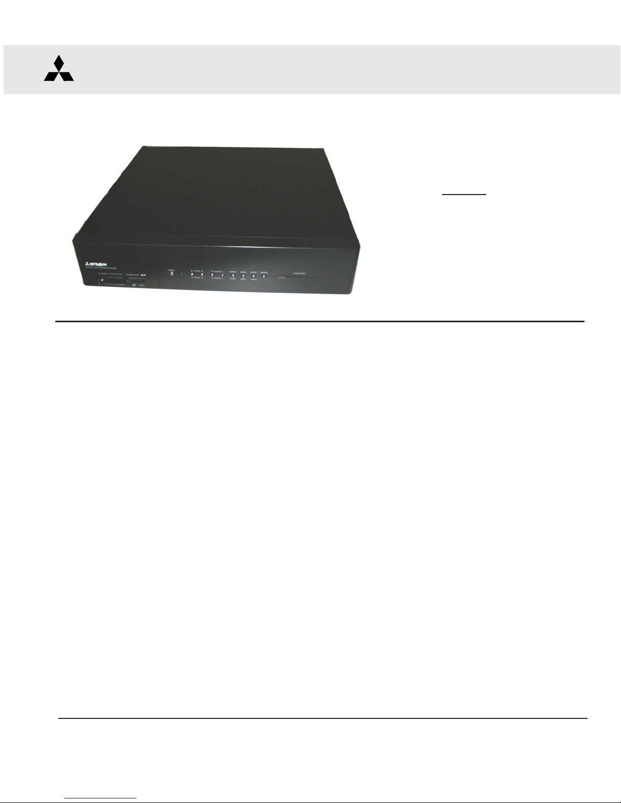
Mitsubishi Electric HD-4001 User manual

CAUTION:
Before servicing this chassis, it is important that the service person read the "SAFETY PRECAUTIONS" and
"PRODUCTSAFETYNOTICE"containedinthismanual.
• Design specifications are subject to change without notice.
MITSUBISHI DIGITAL ELECTRONICS AMERICA, INC.
9351JeronimoRoad,Irvine,CA 92618-1904
Copyright © 2005 Mitsubishi Digital ElectronicsAmerica, Inc.
AllRights Reserved
MITSUBISHIELECTRIC
SerSer
SerSer
Servicevice
vicevice
vice
ManualManual
ManualManual
Manual
20052005
20052005
2005
SET TOP BOX
V26K CHASSIS
SPECIFICATIONS
• Power Input : AC 120V, 60Hz
•Power Usage :82W
• Frequency Range : VHF 54 ~ 470MHz
UHF 470 ~ 806MHz
Analog Cable - 1 ~ 125
Digital Cable - 1 ~ 135
•Antenna Input : 2 RF 75Ω unbalanced
• Tuning : 1NTSC/ATSC/QAM
1 CableCARD™ Slot
1 NTSC for PIP
• Cabinet Dimensions : 17"(W) x 3.7"(H) x 17.25"(D)
• Weight : 12.8 lbs
• Analog Input : VIDEO IN JACK (RCA Type)
Levels 1.0Vp-p 75Ω unbalanced
: AUDIOINJACK (RCAType)
-4.7dBm 43kΩunbalanced
: S-VIDEOINJACK
(Y/C separate type)
Y:1.0 Vp-p C:0.286Vp-p(BURST)
75Ω unbalanced
: COMP/Y, Cr,Cb (RCAType)
Y: 1.0 Vp-p Cr, Cb: 700mVp-p
• Output Level : VIDEOOUTJACK(RCAType)
1.0Vp-p 75Ω unbalanced
: AUDIOOUT JACK (RCAType)
-4.7dBm 4.7kΩ unbalanced
• Digital : IEEE-1394 I/O Jacks
Interface : AC-3 Digtal Audio Output
:HDMI™ Input
: MonitorLinkTM Control/RS-232C
: CableCARD™ Slot
: NetCommand®
.
MODEL
HD-4001
RECEIVER/CONTROLLER
FOR MODELS LT-3280 & LT-3780


MODEL: HD-4001
Page 3
INTRODUCTION ................................................................................................................................5
PRODUCTSAFETYNOTICE ............................................................................................................. 5
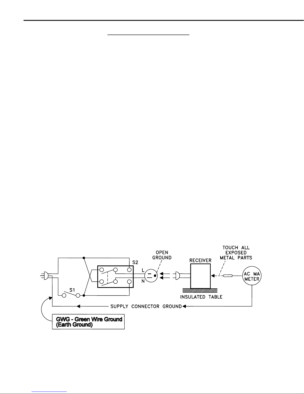
SAFETYPRECAUTIONS ...................................................................................................................6
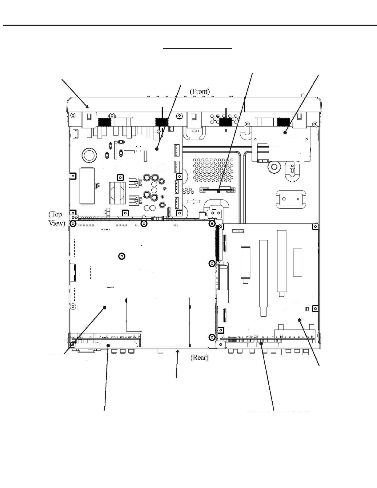
PWB-LOCATIONS .............................................................................................................................7
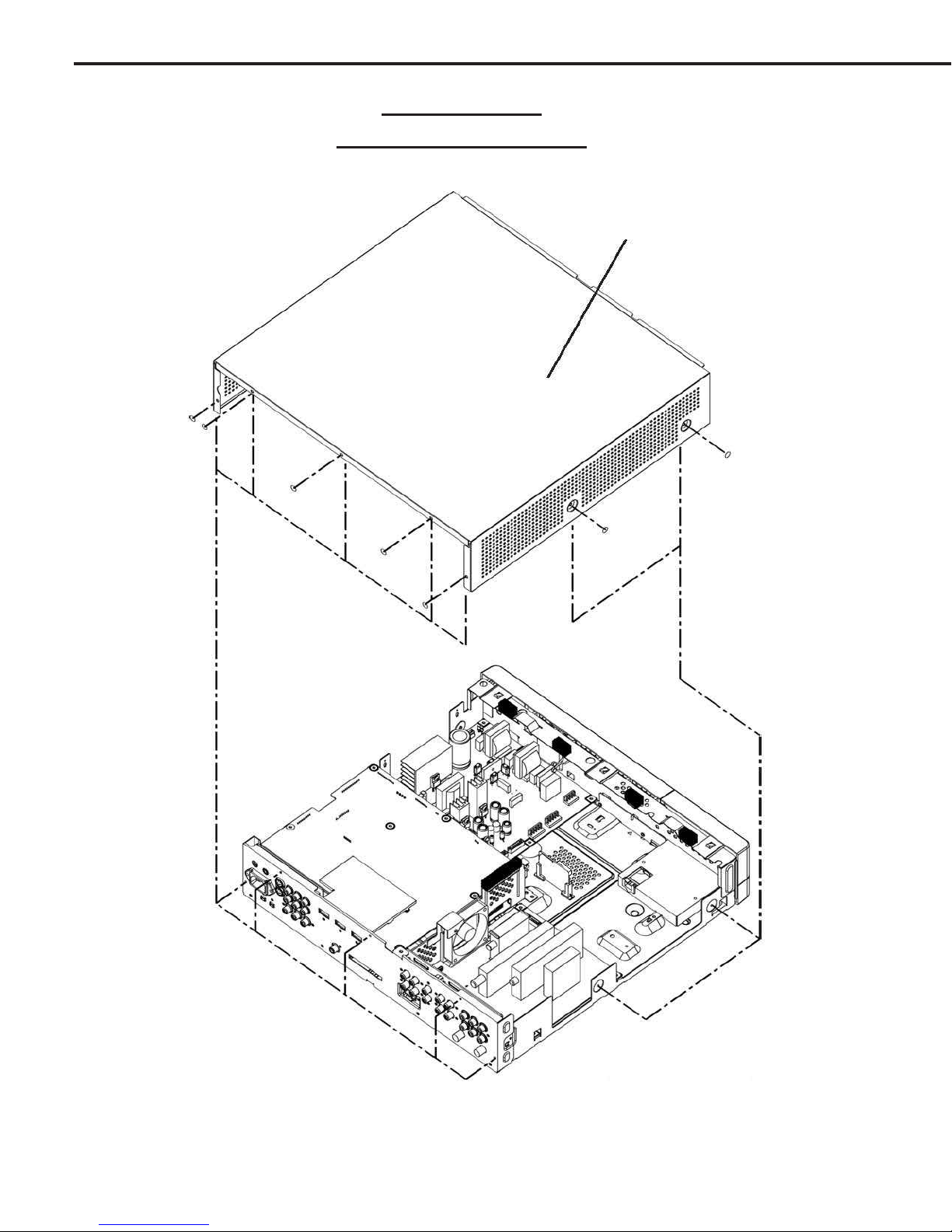
DISASSEMBLY ..................................................................................................................................8
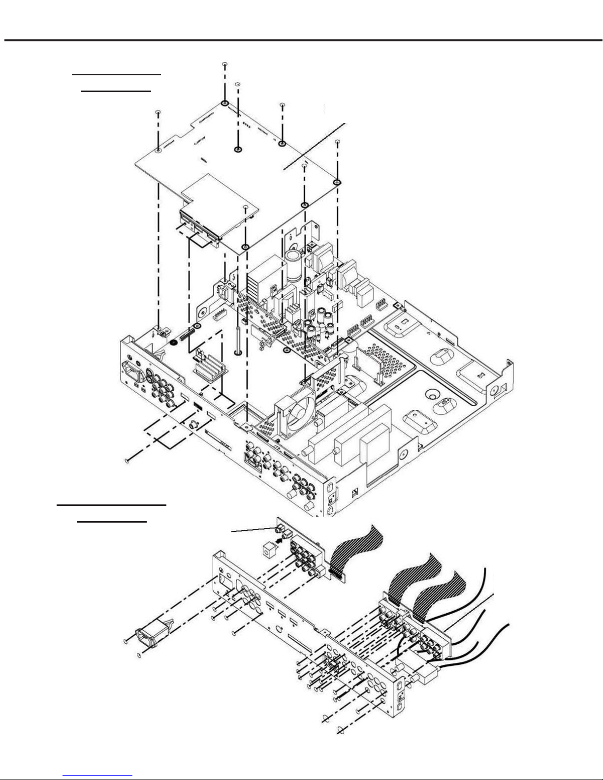
TopCoverremoval ..................................................................................................................8
PWB-SIGNAL& PWB-TERMINALRemoval...........................................................................9
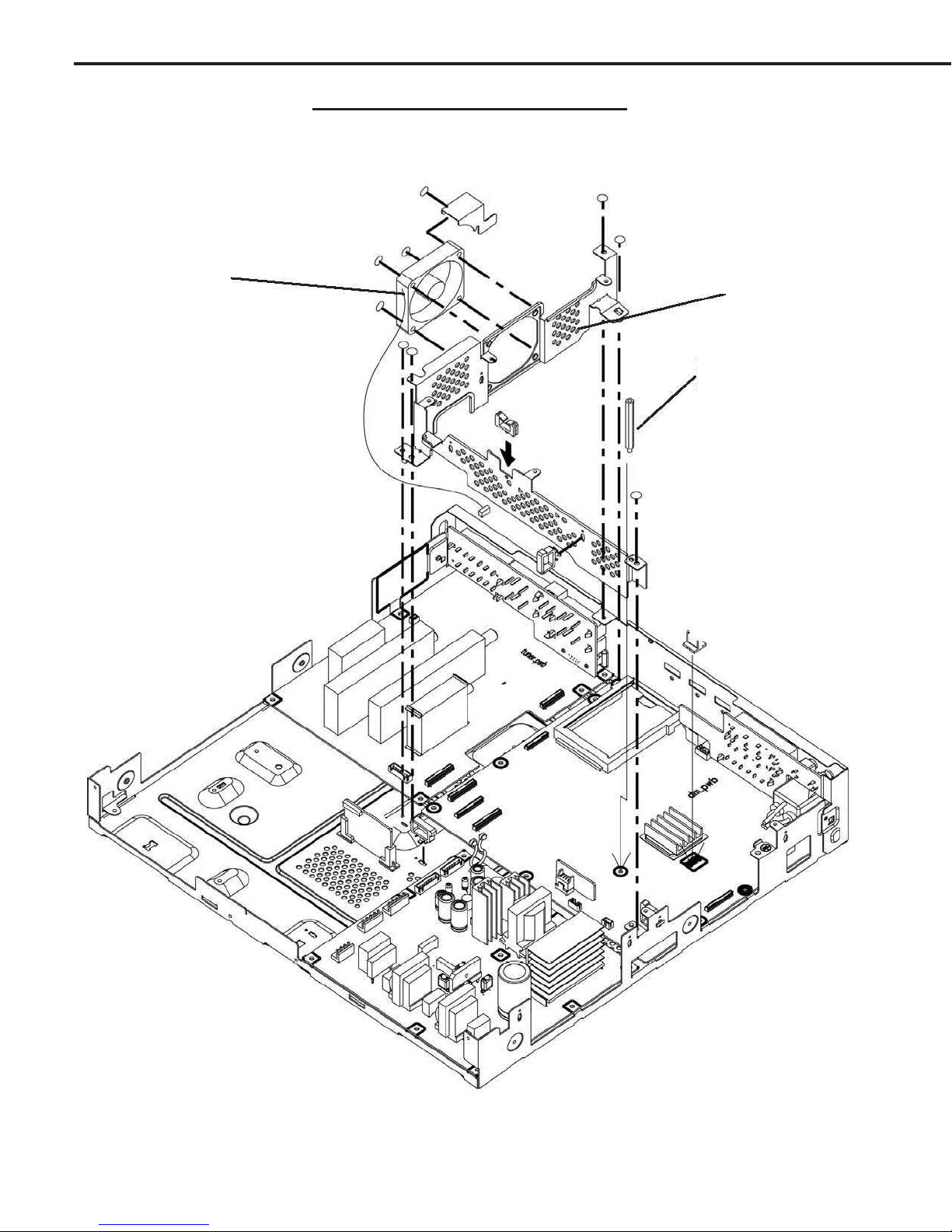
SignalBracket Removal ....................................................................................................... 10
RearPanelRemoval............................................................................................................. 11
CardReader Removal&Front PanelRemovall ..................................................................... 12
ELECTRICALADJUSTMENTS ........................................................................................................ 13
Equipment .................................................................................................................................... 13
Option Menu / Initialization Defaults /AV Defaults ......................................................................... 14
LED Diagnostics ........................................................................................................................... 15
RemoteControl OperationalMode ................................................................................................ 15
CircuitAdjustment Mode ............................................................................................................... 16
Transferingdata ............................................................................................................................ 17
Adjustment Items List................................................................................................................... 17
AdjustmentProcedures ................................................................................................................ 18
Test Points .......................................................................................................................... 18
Main-YGain......................................................................................................................... 18
Sub-YGain .......................................................................................................................... 19
SubPictureOffset ............................................................................................................... 19
CHIPPARTS REPLACEMENT ......................................................................................................... 20
REPLACEMENTPARTS .................................................................................................................. 21
PartsOrdering .............................................................................................................................. 21
CriticalandWarranty Parts Designation........................................................................................21
PartsTolerance Codes.................................................................................................................. 21
SERVICE PARTS LIST .................................................................................................................... 22
CIRCUITRYBLOCK DIAGRAMS ..................................................................................................... 31
StandbyPowerSupplies ............................................................................................................... 31
PWB-DM PowerSupplies ............................................................................................................. 32
PWB-SIGNALSwitchedPowerSupplies ...................................................................................... 32
Tuners &Analog Video Select Circuitry......................................................................................... 33
Digital Video Signal Path .............................................................................................................. 34
Sync Signal Selection................................................................................................................... 35
Sync Signal Output Path .............................................................................................................. 35
SoundSignalPath ........................................................................................................................ 36
Control Circuitry ............................................................................................................................ 37
CommandInput Circuitry............................................................................................................... 38
MacrovisionDetection ................................................................................................................... 38
CONTENTS

Page 4
MODEL: HD-4001
Part 2
Schematic Diagrams
CONTENTS Page
SCHEMATICDIAGRAMS
OverallPWB Interconnect Diagram .................................................................................................1
POWER / E2P / CONTROL / MV Decoder] ....................................................................................2
TERMINAL-1/ TERMINAL-2 [Inputs / Outputs] ...............................................................................3
SIGNAL-1[VideoSwitch]................................................................................................................4
SIGNAL-2[Decoder/Switch]..........................................................................................................5
SIGNALS-3[Micro} .........................................................................................................................6
SIGNAL-4[TVGO] ..........................................................................................................................7
SIGNAL-5[MPEGEncoder]............................................................................................................8
SIGNAL-6[HDMIRX] ...................................................................................................................... 9
SIGNAL-7[HDMITX]..................................................................................................................... 10
SIGNAL-8[Video Output]............................................................................................................. 11
SIGNAL-9[IR232] ......................................................................................................................... 12
TUNER-1[ATSC/NTSCTuner] .................................................................................................... 13
TUNER-2[MainATSC/ NTSC Demodulators] ............................................................................... 14
PWB LAYOUT DIAGRAMS .............................................................................................................. 15

MODELS: HD-4001
Page 5
INTRODUCTION
Thisservice manual providesservice instructions for STBmodel HD-4001which usesthe V26Kchassis. Service
personnelshould read this manualthoroughly before servicingthese chassis.
Thisservice manual includes:
1. SafetyPrecautions
2. Assembly and disassembly instructions.
3. Servicingprintedcircuitboards(PCBs).
4. Electrical adjustments.
5. Chipparts replacement procedures.
6. Circuitpathdiagrams.
The parts list section of this service manual includes:
1. Cabinetandscreenparts.
2. Electrical parts.
Schematicand block diagramsof theabove listedmodels areincluded inthis servicemanual forbetter understanding
of the circuitry. PCB drawings are also included for easy location of parts and test points.
PRODUCT SAFETY NOTICE
Many electrical and mechanical parts in television receivers have special safety related characteristics. These charac-
teristics are often not evident from visual inspection nor can the protection afforded by them necessarily be obtained by
usingreplacement components rated for highervoltage, wattage, etc.
Replacementparts which havespecial safetycharacteristics areidentified inthis servicemanual.
Electrical components having such features are identified by shading on the schematic diagrams and by bold type in
the parts list of this service manual. and by marking on the supplementary sheet for this chassis to be issued subse-
quently. The replacement for any safety part should be identical in value and characteristics.
CableCARDisatrademark of CableTelevisionLaboratories, Inc.
TVGuideOn Screen isa registered trademarkof GemstarDevelopment Corp.
HDMIisatrademarkof HDMI Licensing, LLC.

Page 6
MODELS: HD-4001
SAFETY PRECAUTIONS
NOTICE: Observe all cautions and safety related notes located inside the receiver cabinet and on the
receiverchassis.
WARNING:
1. Operationofthis receiver outside the cabinet or withthe cover removed presents ashock hazard
fromthe receiver's power supplies. Workon the receivershould notbe attempted byanyone who is
notthoroughlyfamiliarwiththeprecautions necessary when working on high voltage equipment.
2. Whenserviceis required, observe the originallead dress. Extra precautionshould be taken to
assure correct lead dress in the high voltage area. Where a short-circuit has occurred, replace those
componentsthat indicate evidence of overheating.
Leakage current check
Before returning the receiver to the customer, it is recommended that leakage current be measured according to the
followingmethods.
1. Cold Check
With the alternating current (AC) plug removed from theAC source, place a jumper across the twoAC plug
prongs. Connect one lead of an ohm meter to theAC plug and touch the other lead to each exposed metal part
(i.e. antennas, handle bracket, metal cabinet, screw heads, metal overlay, control shafts, etc.), particularly any
exposed metal part that has a return path to the chassis. The resistance of the exposed metal parts having a
return path to the chassis should be a minimum of 1Mega Ohm.Any resistance below this value indicates an
abnormalcondition and requires corrective action.
2. Hot Check ...Use the circuit shown below to perform the hot check test.
1. Keep switch S1 open and connect the receiver to the measuring circuit. Immediately after
connection,andwith the switching devices of thereceiver in their operatingpositions, measure
the leakage current for both positions of switch S2.
2. Close switch S1, energizing the receiver. Immediately after closing switch S1, and with the
switchingdevicesofthe receiver in their operating positions, measurethe leakage current for both
positions of switch S2. Repeat the current measurements of items 1 and 2 after the receiver has
reached thermal stabilization. The leakage current must not exceed 0.5 milliampere (mA).

MODELS: HD-4001
Page 7
PWB-LOCATION
PWB
CONTROL PWB
POWER
FAN
PWB CARD
READER
PWB-SIGNAL
(Top)
PWB
TERMINAL1
PWB-DM
(Under Signal)
PWB
TERMINAL2
PWB
TUNER

Page 8
MODELS: HD-4001
DISASSEMBLY
TOP COVER REMOVAL
Top Cover

MODELS: HD-4001
Page 9
PWB-SIGNAL
PWB
SIGNAL
PWB
TERMINAL1
PWB
TERMINAL2
TERMINAL-PWB
REMOVAL
SIGNAL-PWB
REMOVAL

Page 10
MODELS: HD-4001
SIGNAL BRACKET REMOVAL
SIGNAL
BRACKET
PWB
Support
Post
FAN

MODELS: HD-4001
Page 11
REAR PANEL REMOVAL FAN
PWB

Page 12
MODELS: HD-4001
CARD READER REMOVAL
FrontCover
ControlPWB
Frontbracket
FRONT
BRACKET
FRONT
COVER
PWB
CONTROL
(Remove Lower
snaps first)
FRONT PANEL REMOVAL

MODEL: HD-4001
Page 13
ELECTRICAL ADJUSTMENTS
Note: Performonlytheadjustmentsrequired.
Donotattempt an alignment if proper equipmentis not available.
Test Equipment
• Oscilloscope(Unlessotherwise specified, use 10:1 probes)
• SignalGenerator (both SD and HD capable)
Test Signal
A. Monoscope Signal
Note: Ifyoudonothave
amonoscopesignal source,
connect the unit to a VCR
and play a Monoscope
*alignmenttape.
(*Part Number: 859C568060)
B. Color Bar Signal
Use the color bar signal shown
below,unlessotherwisespecified
in this manual.
Monoscope Signal

Page 14
MODEL: HD-4001
DEFAULTS
OPTION MENU
1. Press the “MENU” button on the remote hand unit.
2. Press the buttons “2”, “4”, “7” and “0” in order.
(The screen will change to the option menu.)
Defaults After Initialization Unlock Time :12:00pm
Language :English Background :Gray
Color Balance -- Digital Captions :On if Mute A/V Memory Reset :Ant-1
Side Bar Color :Gray Appearance :Default Audio
Digital Settings Bass :50%
Edit -- Font :Font 3 Treble :50%
Transport Menu :On Size :Large Balance :50%
Default PVR -- Color :White Surround :Off
Icon Order -- Background :Black Listen To (Analog Only) :Stereo
Analog Quality :High Opacity :Translucent Level Sound :On
Background Opacity :Translucent Language (Digital Only) :English
Antenna :1 Video
Memorize -- V-Chiip :Off Contrast :50%
Prefer Digital -- TV Rating :TV-PG Brightness :50%
Channel :3 FV-Fantasy Violence :Enable Sharpness :50%
Memory :Deleted D-Sexual Dialog :Enable Color :50%
Name -- L-Adult Language :Enable Tint :50%
SQV -- S-Sexual Situations :Enable Video noise :Standard
V-Violence :Enable Film Mode (Auto) :On
Clock Setting :Manual Programs Not Rated :Enable Video Mute :On
Time :12:00AM Movie Rating :PG Back Light :100%
Date :1/01/00 V-Chip Time TV Volume :30%
Time Zone :Eastern Start :12:00pm PIP Source :Ant-1 003
Daylight Savings Time :Applies Stop :12:00pm PIP Position :Lower Right
Timer -- POP Position :Right Half
Lock by Time :Off PIP/POP Format :Double Window
Analog Captions :On if Mute Lock Time :12:00pm Format :Stretch
Antenna Menu
Audio / Video
Captions Menu (continued)Setup Menu
NetCommand Menu
Time Menu
Captions Menu Lock by Time
V-Chip Lock Menu
A/V Function Ant 1/2 Input 1/2 Component
1/2 HDMI 1/2 1394
Contrast Center Center Center Center Center
Brightness Center Center Center Center Center
Sharpness Center Center Center Center Center
Color Center Center Center Center Center
Tint Center Center Center Center Standard
V
ideo noise Standard Standard Standard Standard Standard
Backlight Max Max Max Max Max
Film Mode (Auto) On On On On On
Bass Center Center Center Center Center
Treble Center Center Center Center Center
Balance Center Center Center Center Center
Surround Off Off Off Off Off
Listen To Stereo N/A N/A N/A N/A
Level Sound On On On On On
NOTE: User Menu A/V Reset, resets only the selected input A/V settings.

MODEL: HD-4001
Page 15
A. A/V Memory
Each of the external inputs has its’ownAudio/Video Memory. Achange in an A/V setting at a specific input is
stored in memory for that specific input.
B. A/V Reset
TheAV Reset in the user’s menu initializes only the selected input’sA/V Memory.
LED Indicator Diagnostics
The“POWER/TIMER”LED provides an indication of thesets operation, and thepossible cause of a malfunction.
1. Initial Control Circuitry Check
Immediately after theTV is connected to anAC power source:
2. Error Code Operational Check
Note: TheSetTop Box must bein “Shut Down”and not havebeen switched Off,toperform the Error Code
Operational Check. When the unit is switched Off, the code automatically resets to “12” No Error.
Pressing the front panel “DEVICE” and “MENU” buttons at the same time, and holding for 5 seconds,
activates the Error Code Mode. The LED flashes denoting a two digit Error Code, or indicating no problem
has occured since the last Initalization.
Note: The front panel buttons must be used, NOT those on the Remote Control.
•Thenumber of flashes indicates the valueof the MSD(tens digit) of theError Code.
•Theflashingthenpauses for approximately 1/2 second.
•TheLEDthen flashes indicating the valueof the LSD (onesdigit) of theError Code.
•The Error Code is repeated a total of 5 times.
Example: If the Error Code is “23”, the LED will flash two times, pause, and then flash three times.
4. Error Codes
TheError Code designations indicatingmalfunction, orno malfunction,are listed below:
Remote Control Operational Modes
Thereare two Remote HandUnit OperationalModes, “Standard”and “NetCommandTM”. TheRemote isinitially
inthe “Standard”mode. The “NetCommandTM” mode isused when controllingHomeTheater devices using
NetCommandTM. Tochangethe Remote Operational Mode:
•SettheRemotetotheCABLE/DBS/DTVLayer.
•Point the Remote away from the STB.
•Tochange to “NetcommandTM” ... Hold the“Power” button andpress “1-9-7” in sequence.
LED Indications Conditions Probable Cause
Off After AC is applied Standby Power Supply or TV µPC not running
Fast Bllink for 70 sec. After AC is applied Normal DM µPC is booting up
Fast Blink (doesn't stop) After AC is applied DM µPC failed to boot up
Slow Blink Set in Off Normal - Timer is set for Automatic Turn ON
Error Code Probable Cause
12 Normal Operation - No Error Detected
35 Fan Stopped
41 Short Detected

Page 16
MODEL: HD-4001
3.Adjustment Selection
Use the “VIDEO” button to select a specific elecrtrical ajustment.
4.Adjusting Data
After selecting an adjustment item, use the “UP” and “DN” buttons to change adjustment data.
ª If the “UP” button is pressed, the adjustment data increases.
ª If the “DN” button is pressed, the adjustment data decreases.
5. Saving data
Press “ENTER” to save the adjustment data in memory.
The display characters go red for approx. one second in this step.
Note: If the circuit adjustment mode is terminated without pressing
“ENTER”,changes in adjustment data are notsaved.
6. Terminating the circuit adjustment mode
Press the “MENU” button on the remote hand unit twice to terminate the adjustment mode.
Note: Theadjustment mode canbe also terminatedby turningthe
poweroff.
CIRCUIT ADJUSTMENTS
:
ElectricalAdjustments
ElectricalAdjusmentsare performedin ServiceAdjustmentMode.
1.Activating the adjustment mode
1. Press the “MENU” button on a remote hand unit.
(The “MENU” display will appear.)
2. Press the buttons “2”, “4”, “5” and “7” in that order. (The screen will change to the adjustment mode.)
If not changed to the adjustment mode, repeat steps 1 and 2.
2.Adjustment Function Selection
Use the “AUDIO” button to select a specificAdjustment Function.
AD9883A
SMTX MMTX
Functions

MODEL: HD-4001
Page 17
SERVICE MODE - Adjustment Items and Initial Data Values
MAIN MATRIX
Item # Abbrev. Description Data Range Initial Data
1 TNTM Main Tint adjustment 0~63 28
4 COLM Main Color adjustment 0~63 20
14 YDRM Main Y gain control 0~31 5
18 UPDM Main Pb Pedestal adjustment 0~15 7
19 VPDM Main Pr Pedestal adjustment 0~15 7
SUB MATRIX
Item # Abbrev. Description Data Range Initial Data
1 TNTS Sub Tint adjustment 0~63 28
4 COLS Sub Color adjustment 0~63 18
14 YDRS Sub Y gain control 0~31 5
18 UPDS Sub Pb Pedestal adjustment 0~15 7
19 VPDS Sub Pr Pedestal adjustment 0~15 7
Transferring Data
1) Enterthe ServiceAdjustmentMode... Press “MENU-2-4-5-7”
2) Press “0” when in the Service Mode ... Three choices appear at the top of the screen.
3) User UP & DN keys to highlight the desired choice, the Press “ENTER”
Display Description
Backup DVC files to CF Copies Alignment data to compact flash
Restore DVC files from CF Loads Alignment data from compact flash
Copy WB Alignment Used to transfer WB data from signal E2P to DM E2P
Data Transfer Definitions
AD9883
A
Item # Abbrev. Description Data Range Initial Data
12 ROFF Red Offset 0~127 55
14 BOFF Blue Offset 0~127 59

MODEL: HD-4001
Page 18
Purpose:
Measuring
Instrument
Test Point
Measuring
Range
Input Signal
Ext. Trigger
Input Terminal
Symptom:
Purpose:
Measuring
Instrument
Test Point
Measuring
Range
Input Signal
Ext. Trigger
Input Terminal
Symptom:
[Video Circuit]
1. Main-Y Gain
To set the main picture Ylevel
Incorrectanalogsourcemainpicturebrightnesslevel.
Oscilloscope
TPMY
------
-------
Color bars
External Input
1. Supply a Color Bars with 100% white signal to an External Input.
2. Connect a scope to TPY.
3. Enter the Alignment Mode (MENU-2-4-5-7)
4. Select the MMTX function (AUDIO button).
5. Select adjust item #14 YDRM (VIDEO button).
6. Set the data so the waveform at TPY is 0.7 Vp-p ±0.03 Vp-p (ADJUST buttons).
7. Press “ENTER” to save data.
8. Press “MENU” twice to exit the service mode.
TEST POINTS
TPSY TPY
TPSY TPY
PWB-SIGNAL (Partial)

MODEL: HD-4001
Page 19
Purpose:
Measuring
Instrument
Test Point
Measuring
Range
Input Signal
Ext. Trigger
Input Terminal
Symptom:
Purpose:
Measuring
Instrument
Test Point
Measuring
Range
Input Signal
Ext. Trigger
Input Terminal
Symptom:
[Video Circuit]
3. Sub Picture Offset
To match sub picture white to main picture white
Subpicture white differsfrom whitein themain picture.
----
----
------
-------
Full White Raster
External Input
1. Supply a full white raster signal to an External Input.
2. Select the white raster as the source for both the main and sub pictures.
3. Use the PIP/POP buttion to select the Single PIP mode.
4. Enter the Alignment Mode (MENU-2-4-5-7)
4. Select the AD9883A function (AUDIO button).
5. Select item #12 ROFF and #14 BOFF (VIDEO button).
6. Set the data fore items #12 and #14 so the sub picture white is close to that in
the main picture. (ADJUST buttons).
7. Press “ENTER” to save data.
8. Press “MENU” twice to exit the service mode.
[Video Circuit]
2. Sub-Y Gain
To set the sub picture Ylevel
Incorretanalogsourcesibpicturebrightness level.
Oscilloscope
TPSY
------
-------
Color bars
External Input
1. Supply a Color Bars with 100% white signal to an External Input. Select this
input as the sub picture source.
2. Connect a scope to TPSY.
3. Enter the Alignment Mode (MENU-2-4-5-7)
4. Select the SMTX function (AUDIO button).
5. Select adjust item #14 YDRS (VIDEO button).
6. Set the data so the waveform at TPSY equals the main-y signal. (ADJUST
buttons).
7. Press “ENTER” to save data.
8. Press “MENU” twice to exit the service mode.
TPSY TPY
PWB-SIGNAL (Partial)

PAGE20
MODELS: HD-4001
CHIP PARTS REPLACEMENT
Some resistors, shorting jumpers (0 Ohm resistors),
ceramic capacitors, transistors and diodes are chip parts.
Thefollowing precautions should be taken when replacing
these parts.
Cautions:
1. Usea fine tipped, wellinsulated soldering iron
(approximately30watts), and tweezers.
2. Meltthe solder andremove thechip parts
carefully so as not to tear the copper foil from
theprintedcircuit board.
3. Discardremoved chips; do notreuse them.
4. Donot apply heat formore than 3(three)
seconds to new chip parts.
5. Avoidusing a rubbing stroke when soldering.
6. Take care not to scratch, or damage the chip
partswhen soldering.
7. Supplementarycementing is not required.
Chip Parts Removal (Resistors, Capacitors, etc.)
1. Grasp the part with tweezers. Melt the solder
atboth sides alternately, and remove oneside
of the part with a twisting motion.
2. Melt the solder at the other side and remove
thepart.
Chip Parts Removal (Transistors)
1. Melt the solder of one lead and lift the side of
thatlead upward.
2. Simultaneously melt the solder of the other
two leads and lift the part from the PCB.
Replacement
1. Presolder the contact points on the circuit
pattern.
2. Pressthe part downward with tweezers and
applythe soldering ironas shown.
Table of contents
Other Mitsubishi Electric Receiver manuals
Popular Receiver manuals by other brands

Aiphone
Aiphone RY-IP44 Programming manual

Sony
Sony HCD-C770 - Hi Fi Components Service manual

PCB Piezotronics
PCB Piezotronics TLD356B18 Installation and operating manual

Harman Kardon
Harman Kardon AVR 520 Service manual

Marantz
Marantz SR7500 Service manual

Quark-Elec
Quark-Elec QK-A026 Quick start setup guide