NAD T562 User manual

NAD
SERVICE MANUAL
T 562
T 562
DVD / VCD / CD
PLAYER
DVD / VCD / CD
PLAYER
DRAFT DATE: 30 OCT, 2002

SECTION 1
SUMMARY
CONTENTS
PRODUCT SAFETY SERVICING GUIDELINES FOR VIDEO PRODUCTS …………… 1-4
SERVICING PRECAUTIONS…………………………………………………………………1-5
*General Servicing Precautions
*Insulation Checking Procedure
*Electrostatically Sensitive Devices
SPECIFICATIONS ……………………………………………………………………….…...1-6
LOCATION OF CUSTOMER CONTROLS…………………………………………….1-7~1-8
EXPLODED VIEWS…………………………………………………………………….1-9~1-10
PACKING DIAGRAM………………………………………………………………….1-11~1-12

1-4
PRPDUCT SAFETY SERVICING GUIDELINES FOR VIDEO PRODUCTS
CAUTION: DO NOT ATTEMPT TO MODIFY THIS PRODUCT IN
ANYWAY. NEVER PERFORM CUSTOMINIZED INSTALLATIONS
WITHOUT MANUFACTURER’ S APPROVAL. UNAUTHORIZED
MODIFICATIONS WILL NOT ONLY VOID THE WARRANTY, BUT MAY
LEAD TO YOUR BEING LIABLE FOR ANY RESULTING PROPERTY
DAMAGE OR USER INURY.
SERVICE WORK SHOULD BE PERFORMED ONLY AFTER YOU ARE
THOROUGHLY FAMILIAR WITH ALL OF THE FOLOWING SAFETY
CHECKS AND SERVICING GUIDELINS. TO DO OTHERWISE,
INCREASES THE RISK OF POTENTIAL HAZARDS AND INJURY TO
THE USER.
WHILE SERVICING, USE AN ISOLATION TRANSFORMER FOR
PROTECTION FROM A.C. LINE SHOCK.
SAFETY CHECKS
AFTER THE ORIGINAL SERVICE PROBLEM HAS BEEN CORRCTED,
A CHECK SHOULD BE MADE OF THE FOLLOWING.
SUBJECT: FIRE &SHOCK HAZARD
1. BE SURE THAT ALL COMPONENTS ARE POSITIONED IN SUCH A
WAY AS TO AVOID POSSIBILITY OF ADJACENT COMPONET SHORTS.
THIS IS ESPECIALLY IMPORTANT ON THOSE MODULES WHICH ARE
TRANSPORTED TO AND FROM THE REPAIR SHOP.
2. NEVER RELEASE A REPAIR UNLESS ALL PROTECTIVE DEVICES
SUCH AS INSULATORS, BARRIERS, COVERS, SHIELDS, STRAIN
RELIEFS, POWER SUPPLY CORDS, AND OTHER HARDWARE HAVE
BEEN REINSTALLED PERORIGINAL DESIGN. BE SURE THAT THE
SAFETY PURPOSE OF THE POLARIZED LINE PLUG HAS NOT BEEN
DEFEATED.
3. SOLDERING MUST BE INSPECTED TO DISVCOVER POSSIBLE
COLD SOLDER JOINTS, SOLDER SPLASHES OR SHARP SOLDER
POINTS. BE CERTAIN TO REMOVE ALL LOOSE FOREIGN PARTICLES.
4. CHECK FOR PHYSICAL EVIDENCE OF DAMAGE OR
DETERRIORATION TO PARTS AND COMPONENTS. FOR FRAYED
LEADS, DAMAGED INSULATION (INCLUDING A.C. CORD).AND
REPLACE IF NECESSARY FOLLOW ORIGINAL LAYOUT, LEAD
LENGTH AND DRESS.
5. NO LEAD OR COMPONENT SHOULD TOUCH A RECIVING TUBE
OR A RESISTOR RATED AT 1 WATT OR MORE. LEAD TENSION
AROUD PROTRUNING METAL SURFACES MUST BE AVOIDED.
6. ALL CRITICAL COMPONENTS SUCH AS FUSES, FLAMEPRO OF
RESISTORS, CAPAICTORS, ETC. MUST BE REPLACED WITH EXACT
FACTORY TYPES. DO NOT USE REPLACEMENT COMPONETS
OTHER THAN THOSE SPECIFIED OR MAKE UNRECOMMENDED
CIRCUIT MODIFICATIONS.
7. AFTER RE-ASSEMBLY OF THE SET ALWAYS PERFORM AN A.C.
LEAKAGE TEST ON ALL EXPOSED METALLIC PARTS OF THE
CABINET, (THE CHANNEL SELECTOR KNOB, ANTENNA TERMINALS.
HANDLE ADN SCREWS) TO BE SURE THE SET IS SAFET TO
OPERATE WITHOUT DANGER OF ELECTRICAL SHOCK. DO NOT USE
A LINE ISOLATION TRANSFORMER DURING THIS TEST USE AN A.C.
VOLTMETER, HAVING 5000 OHMS PER VOLT OR MORE SENSITIVITY,
IN THE FOLLOWING MANNER; CONNECT A 1500OHM 10 WATT
RESISTOR, PARALLELED BY A. 15 MFD, 150.V A.C. TYPE CAPACITOR
BETWEEN A KNOWN GOOD EARTH GROUND (WATER PIPE,
CONDUIT, ETC.) AND THE EXPPOSED METALLIC PARTS, ONE AT A
TIME.
MEASURE THE A.C. VOLTAGE ACROSS THE COMBINATION OF 1500
OHM RESISTOR AND .15 MFD CAPACITOR.
REVERSE THE A.C. PLUG AND REPEAT A. C. VOLTAGE
MEASUREMENTS FOR EACH EXPOSED METALLIC PART.
VOLTAGE MEASURE MUST NOT EXCEED 75 VOLTS R.M.S. THIS
CORRESPONDS TO 0.5 MILLIAMP A.C. ANY VALUE EXCEEDING THIS
LIMIT CONSTITUTED A POTENTIAL SHOCK HAZARD AND MUST BE
CORRECTED IMMEDIATELY.
SUBJECT: GRAPHIC SYMBOLS
SUBJECT: TIPS ON PROPER INSTALLATION
1. NEVER INSTALL ANY PRODUCT IN A CLOSED-IN RECESS,
CUBBYHOLE OR CLOSELY FITTING SHELF SPACE. OVER OR
CLOSE TO HEAT DUCT, OR IN THE PATH OF HEATED AIR
FLOW.
2. AVOID CONDITIONS OF HIGH HUMIDITY SUCH AS:
OUTDOOR PATIO INSTALLATIONS WHERE DEW IS A FACTOR,
NEAR STEAM RADIATORS WHERE STEAM LEAKAGE IS
FACTOR, ETC.
3. AVOID PALCEMNET WHERE DRAPERIES MAY OBSTRUCT
REAR VENTING. THE CUSTOMER SHOULD ALSO AVOID THE
USE OF DECORATIVE SCARVES OR OTHER COVERINGS
WHICH MIGHT OBSTRUCT VENTILATION.
4. WALL AND SHELF MOUNTED INSTALLATIONS USING A
COMMERCIAL MOUNTING KIT. MUST FOLLOW THE FACTORY
APPROVED MOUNTING INSTRUCTIONS A PRODUCT
MOUNTED TO A SHELF OR PLATFORM MUST RETAIN ITS
ORIGINAL FEET (OR THE EQUIVALENT THICKNESS IN
SPACERS) TO PROVIDE ADEQUATE AIP FLOW ACROSS THE
BOTTOM, BOLTS OR SCREWS USED FOR FASTENERS MUST
NOT TOUCH ANY PARTS OR WIRING. PERFORM LEAKAGE
TEST ON CUSTOMIZED INSTALLATIONS.
5. CAUTION CUSTOMERS AGNINST THE MOUNTING OF A
PRDUCT ON SLOPING SHELF OR TILTED POSITION, UNLESS
THE PRODUCT IS PROPERLY SECURED.
6. A PRODUCT ON A ROLL-ABOUT CART SHOULD BE STABLE
ON ITS MOUNTING TO THE CART. CAUTION THE CUSTOMER
ON THE HAZARDS OF TRYING TO ROLL A CART WITH SMALL
CASTERS ACROSS THRESHOLDS OR DEEP POLE CARPETS.
7. CAUTION CUSTOMERS AGAINST THE USE OF A CART OR
STAAND WHICH HAS NOT BEEN LISTED BY UNDERWRITERS
LABORATORIES, INC. FOR USE WITH THEIR SPECIFIC
MODEL OF THELVISION RECEIVER OR GENERICALLY
APPROVED FOR USE WITH T.V.’S OF THE SAME OR LARGER
SCREEEN SIZE.
8. CAUTION CUSTOMERS AGAINST THE USE OF EXTENSION
CORDS, EXPLAIN THAT A FOREST OF EXTENSIONS
SPROUTING FROM A SINGAL OUTLET CAN LEAD TO
DISASTROUS CONSEQUENCES TO HOME AND FAMILY.
THE LIGHTNING FASH WITH ARROWHEAD SYMBOL, WITHIN AN
EQUILATE
RAL TRIANGLE, IS INTENDED TO ALERT THE USER TO THE
PRESENCE OF UNINSULATED “DANGEROUS VOLTAGE”
WITHIN THE
PRODUCT’
S ENCLOSURE THAT MAY BE OF SUFFCIENT MAGNITUDE TO
CONSTITUTE A RISK OF ELECTRIC SHOCK.
THE EXCELAMATION POINT WITHIN AN EQUILATERAL TRIANGLE
IS
INTENDED TO ALERT THE USER TO THE PRESENCE OF IMPORANT
OPERATING AND MAINTENANCE (SERVICING) INSTRUCTIONS IN THE
LITERATURE ACCOMPANYING THE APPLIANCE.

1-5
SERVICING PRECAUTIONS
CAUTION:
Before servicing the DVD player covered by this service
data and its supplements and addends, read and follow
the SAFETY PRECAUTIONS. NOTE: if unforeseen
circumstances create conflict between the following
servicing precautions and any of the safety precautions in
this publications, always follow the safety precautions.
Remembers Safety First:
General Servicing Precautions
1. Always unplug the DVD player AC power cord from the AC
power source before:
(1) Removing or reinstalling any component, circuit board,
module, or any other assembly.
(2) Disconnection or reconnecting any internal electrical
plug or other electrical connection.
(3) Connection a test substitute in parallel with an
electrolytic capacitor.
Caution:A wrong part substitution or incorrect polarity
installation of electrolytic capacitors may result in an
explosion hazard.
2. Do not spray chemicals on or near this DVD player or
any of its assemblies.
3. Unless specified otherwise in this service data, clean
electrical contacts by applying an appropriate contact
cleaning solution to the contacts with a pipe cleaner,
cottontipped swab, or comparable soft applicator.
Unless specified otherwise in this service data, lubrication
of contacts is not required.
4. Do not defeat any plug/socket B+ voltage interlocks
with which instruments covered by this service manual
might be equipped.
5. Do not apply AC power to this DVD player and/or any
of its electrical assemblies unless all solid-state device
heat sinks are correctly installed.
6. Always connect test instrument ground lead to the
appropriate ground before connection the test instrument
positive lead. Always remove the test instrument ground
lead last.
Insulation Checking Procedure
Disconnect the attachment plug from the AC outlet and
turn the power on. Connect an insulation resistance
meter (500V) to the blade of the attachment plug. The
insulation resistance between each blade of the
attachment plug and accessible conductive parts (Note 1)
should be more than 1M-ohm.
Note 1: Accessible Conductive Parts including Metal
panels, Input terminals, Earphone jacks, etc.
Electrostatically Sensitive (ES) Devices
Some semiconductor (solid state) devices can be damaged
easily by static electricity. Such components commonly are
called Electrostatically Sensitive (ES) Devices. Examples of
typical Es devices are integrated circuits and some field
effect transistors and semiconductor chip components.
The following techniques should be used to help reduce the
incidence of component damage caused by static electricity.
1.Immediately before handing any semiconductor
component or semiconductor equipped assembly, drain
off any electrostatic charge on your body by touching a
known earth ground. Alternatively, obtain and wear a
commercially available discharging wrist strap device,
which should be removed for potential shock reasons
prior to applying power to the unit under test.
2.After removing an electrical assembly equipped with ES
devices, place the assembly on a conductive surface such
an aluminum foil, to prevent electrostatic charge buildup
or exposure of the assembly.
3.Use only a grounded-tip soldering iron to solder or
unsolder ES devices.
4.Use only an antistatic solder removal device. Some
solder removal devices not classified an “antistati c” can
generate electric charges sufficient to damage ES
devices.
5.Do not use freonpropelled chemicals. These can
generate electrical charge sufficient to damage ES
devices.
6.Do not remove a replacement ES device from its protect
tive package until immediately before you are ready to
install it. (Most replacement ES devices are packaged
with leads electrically shorted together by conductive
foam, aluminum foil, or comparable conductive material).
7.Immediately before removing the protective material
from the leads of a replacement ES device, touch the
protective material to the chassis or circuit assembly into
which the device will be installed.
Caution: Be sure no power is applied to the chassis or
circuit, and observe all other safety precautions.
8.Minimize bodily motions when handing unpackaged
replacement ES devices. (Normally harmless motion
such as the brushing together of your clothes fabric or
the lifting of your foot from a carpeted floor can generate
static electricity sufficient to damage an ES device.)

1-6
SPECIFICATIONS
DVD VIDEO PLAYER
POWER SUPPLY……………………………………………… AC 230V,50Hz (EUR)/120V,60Hz(US/CANADA)
Power consumption…………………………………………. 30W
External dimensions………………………………………… 435×80×280mm
Weight (net)…………………………………………………… 4.6kg
Signal system…………………………………………………. PAL (EUR)/NTSC (USA/CANADA)
Laser……………………………………………………………. Semiconductor laser, wavelength 650nm
Frequency range(digital audio)…………………………….. 2Hz to 22kHz
Signal-to-noise………………………………………………… More than 102dB(A-WEIGHTED)
Audio dynamic ……………………………………………….. More than 92dB
Harmonic distortion………………………………………….. 0.008%
Operating conditions…………………………………………. Temperature: 41°to 95°, operation status: Horizontal
OUTPUTS
Video output …………………………………………………… 1.0V (p-p), 75Ù, negative sync., RCA jack×1
S-video output…………………………………………………. (Y) 1.0V (P-P), 75Ù,negative sync., Mini DIN 4pin×1
(C) 0.286V (P-P), 75Ù
Component Video output …………………………………… (Y)1.0V (P-P), 75Ù,negative sync.,
(Cb Cr) 0.5V (P-P), 75Ù
Scart Video output…………………………………………….. (CVBS)1.0V(P-P) ,75Ù,negative sync.,
(R GB)0.7V(P-P),75Ù
Audio output(digital audio) ………………………………….. 0.5V(p-p) 75Ù, RCA jack×1
Audio output(analog audio) …………………………………. 2.0Vrms(1kHz, 0dB), RCA jack×1

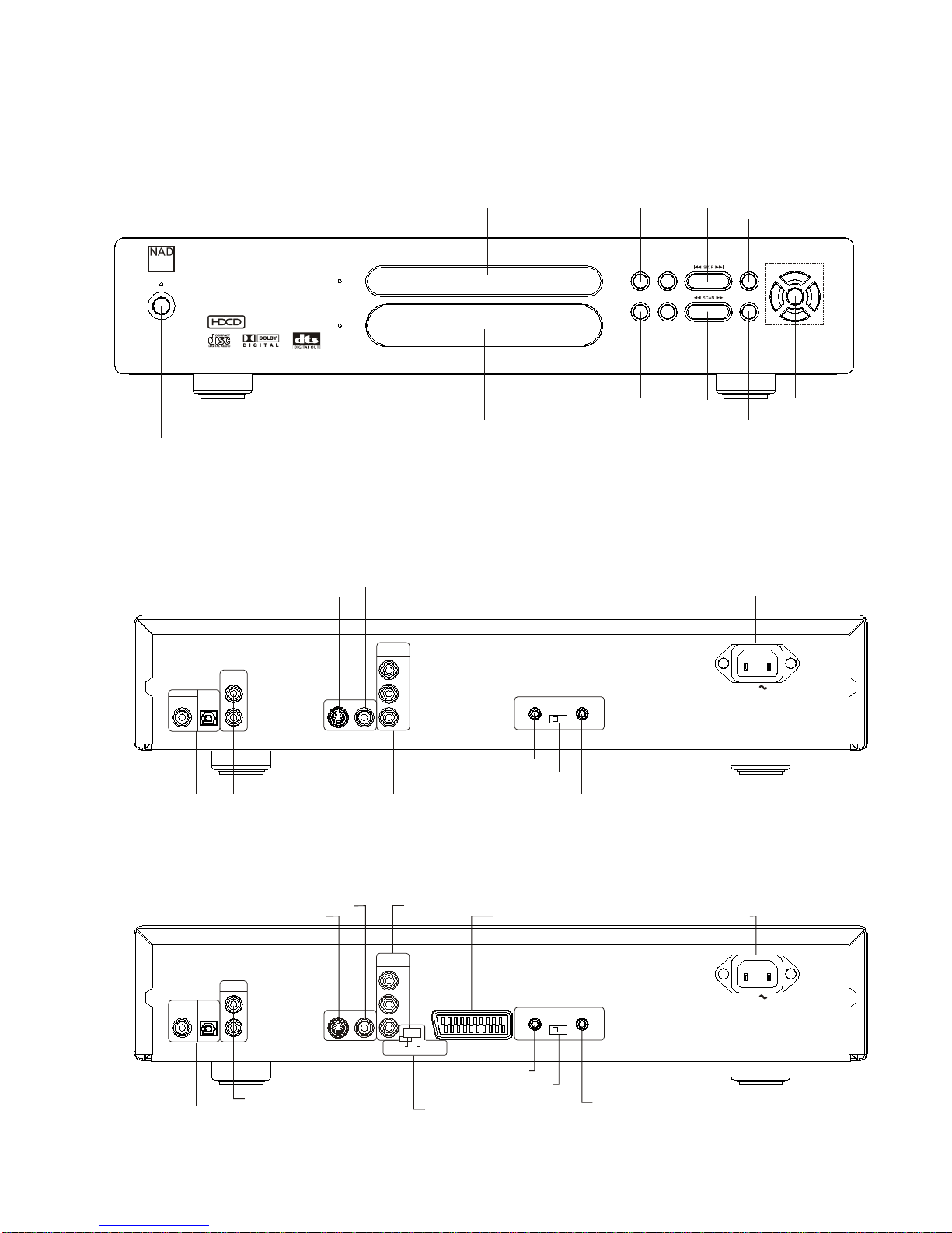
PLAY PAUSE
OPEN/CLOSE STOP PROGRESSIVE
SCAN
MENU SELECT
DVD / CD / MP3 Player T 562
POWER/Standby button
and indicator
(Standby mode: Ambercolor)
Disc Tray
Display Window
Progressive Scan LED
HDCD LED
PLAY Button
PAUSE Button
SKIP Button
MENU Button
SELECT Button
PROGRESSIVE SCAN Button
SCAN Button
STOP Button
OPEN/CLOSE Button
OPTICAL
DIGITAL OUT
COAXIAL
MIXED
AUDIO OUT
VIDEO OUT
AC IN
S VIDEO
COMPONENT
VIDEO OUT
Y
Cb
Pb
Cr
Pr
L
R
AUTO TRIGGER
+12V TRIGGER IN EXT. IR IN
ON OFF
OPTICAL
DIGITAL OUT
COAXIAL
MIXED
AUDIO OUT
AC IN
L
R
AUTO TRIGGER
+12V TRIGGER IN EXT. IR IN
ON OFF
VIDEO OUT
SCART/RGB OUT
S VIDEO
SCART/RGB
S-VIDEO
OUTPUT
VIDEO
COMPONENT
VIDEO OUT
Y
Cb
Pb
Cr/Pr
DIGITAL AUDIOOUT Jacks
AUDIO MIXED OUTJacks
S-VIDEO OUT Jacks
COMPOSITE VIDEO OUTJacks
COMPONENT VIDEO OUTJacks
12V TRIGGER INJACK
AUTO TRIGGER SWITCH
EXT.IR IN Jacks
AC INLETS
DIGITAL AUDIOOUT Jacks
AUDIO MIXED OUTJacks
S-VIDEO OUT Jacks
COMPOSITE VIDEO OUTJacks COMPONENT VIDEO OUTJacks
12V TRIGGER INJACK
AUTO TRIGGER SWITCH
EXT.IR IN Jacks
AC INLETS
SCART/RGB OUT JACK
VIDEO OUTPUT Switch
(S-VIDEO /SCART/RGB)
FRONT PANEL
REAR PANEL
AH VERSION (US/CANADA)
C VERSION (EUROPEAN)
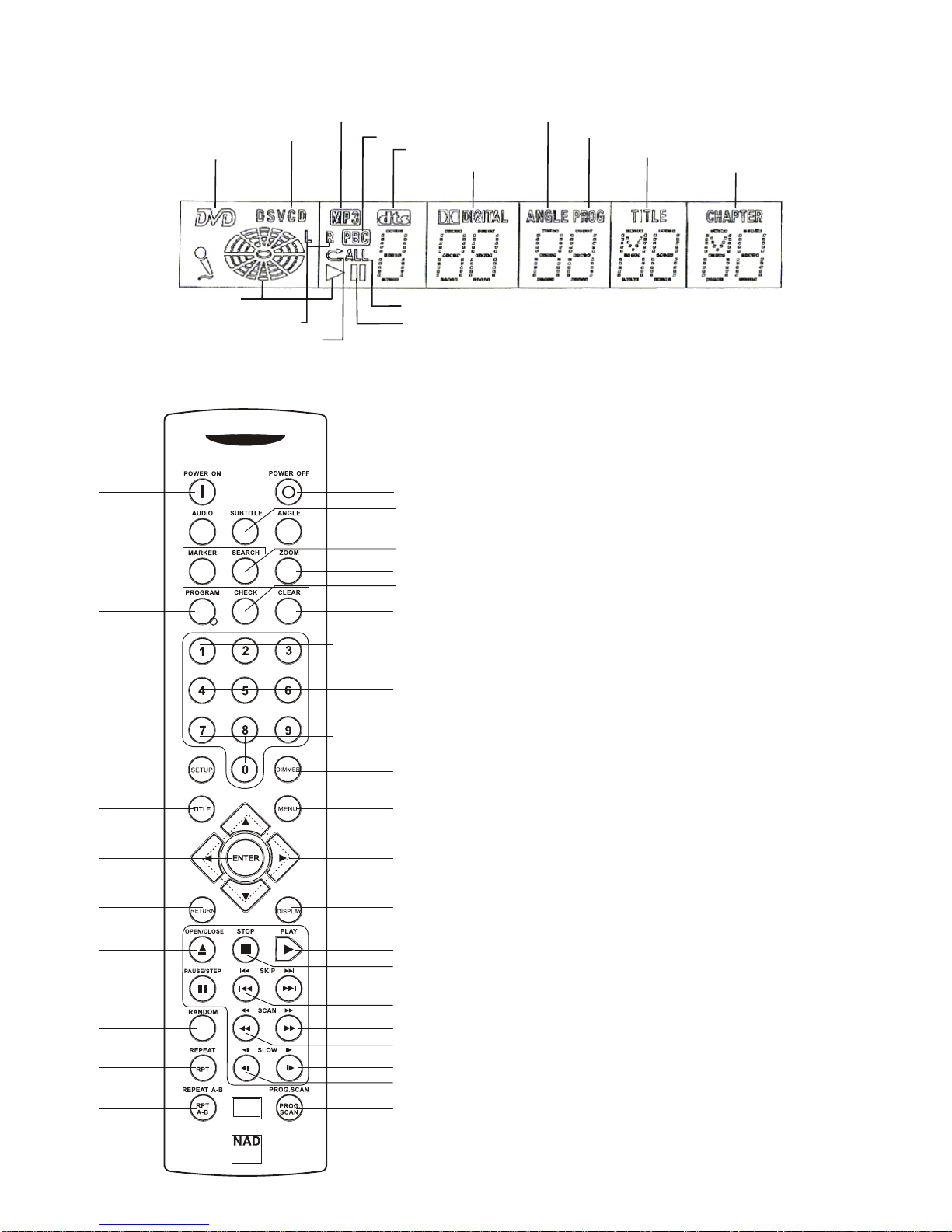
LOCATION OF CUSTOMER CONTROLS

DVD3
1.POWER ON Button
2.POWER OFF Button
3.SUBTITLE Button
4.AUDIO Button
5.ANGLE Button
6.SEARCH Button
7.MARKER Button
8.ZOOM Button
9.CHECK Button
10.PROGRAM Button
11.CLEAR Button
12.NUMERIC Buttons
13.SETUP Button
14.DIMMER Button
15.TITLE Button
16.MENU Button
17.ENTER Button
18.ARROW Buttons
19.RETURN Button
20.DISPLAY Button
21.OPEN/CLOSE Button
22.STOP Button
23.PLAY Button
24.PAUSE/STEPButton
25.REV SKIP Button
26.FWD SKIP Button
27.REV SCAN Button
28.FWD SCAN Button
29.REW SLOW Button
30.RANDOM Button
31.FWD SLOW Button
32.REPEAT Button
33.PROGRESSIVE SCAN Button
34.REPEAT A-B Button
1
4
2
3
5
6
8
9
11
7
10
12
14
13
15 16
17 18
19 20
21
24
22
23
25
26
27
28
29
31
33
30
32
34
DVD Indicator
VCD Indicator
MP3 Indicator
PBC Indicator
DTS Indicator
PLAY Indicator
L&R CHNNEL Indicator
REPEAT TRACK Indicator
REPEAT All Indicator
PAUSE Indicator
CHARTER Indicator
TITLE Indicator
PROGRAM Indicator
ANGLE Indicator
DIGITAL Indicator
DISPLAY WINDOW
REMOTE CONTROL

F 001F 001
F 002
F 003 000 400 04
F 004F 004
000 100 01 F 00 5F 00 5
F 006
F 008F 008
F 007F 007
S 005S 00 5
S 006S 00 6
S 006S 00 6
S 006S 00 6
F 009F 009
F 009F 009
F 009F 009
S 002S 00 2 C 014C 014
C 013C 013
000 100 01
000 300 03
S 007S 00 7
S 001S 00 1
S 003
C 002C 002
C 003C 003
C 004C 004
S 004S 00 4
000 100 01 C 01 0
000 600 06
000 100 01
000 600 06
000 200 02
000 1
C 008C 008
C 009
000 100 01
000 100 01
C 007C 007
C 015C 015
C 006C 006
C 005C 005
C 013C 013
C 014C 014
000 100 01
000 100 01
000 600 06
000 200 02
000 600 06
C 001C 001
000 500 05
000 100 01
000 400 04 00 010 001
S 001S 00 1
T0 01T 00 1
000 100 01
000 300 03
F 004F 004
000 400 04
000 1
C 009C 009
C 011C 011
C 012C 012 0002000 2
S 002S 00 2
000 200 02
000 100 01
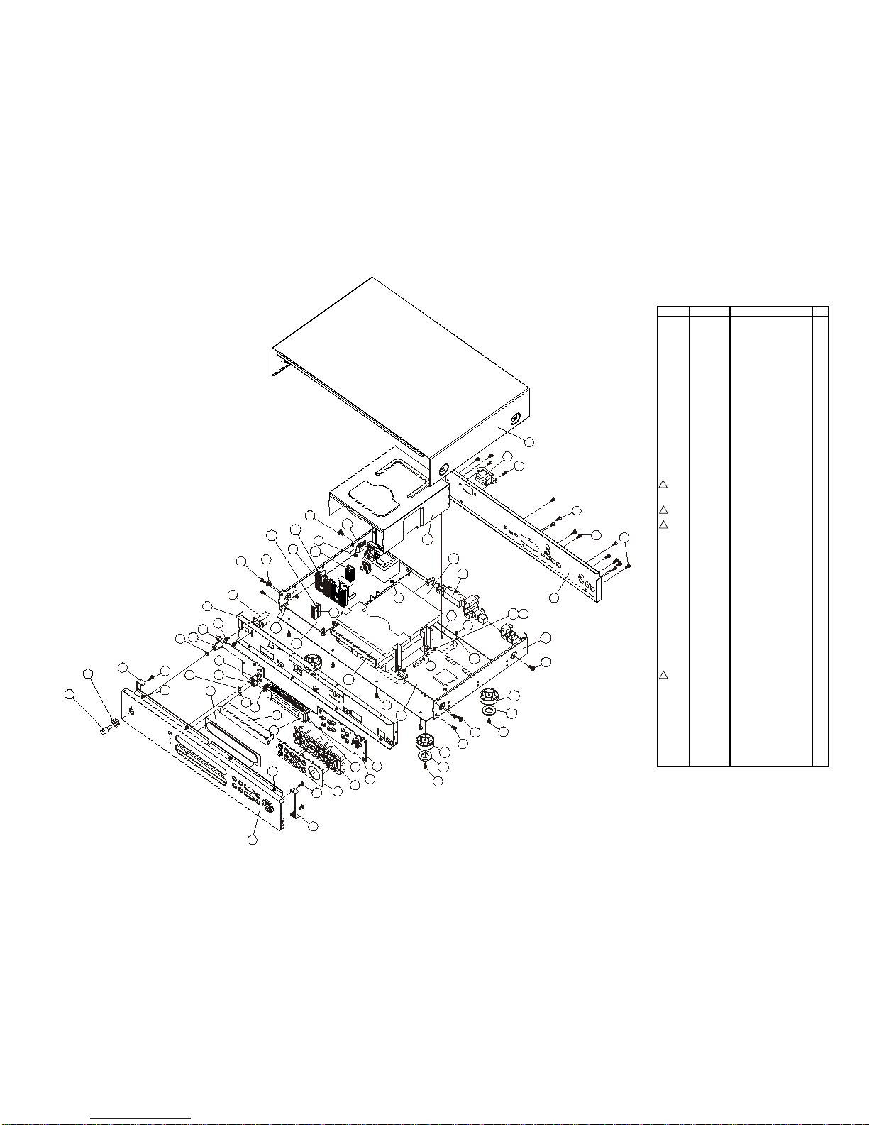
EXPLODED VIEW T562
Qty.
F 00 1 67-009001-0 F a sc ia (C V e rsion) 1
67-009002-0 F as c ia (A H V ers ion) 1
F 00 2 77-009003-0 P ower B utton 1
F 00 3 77-001007-0 P ower B utton B e ze l 1
F 00 4 66-009007-0 E nd C a p 2
F 00 5 76-009001-0 Window 1
F 00 6 77-009002-0 C D Door 1
F 00 7 75-009001-0 C urs or B utton B ez el 1
F 00 8 77-009001-0 C urs or B utton 1
F 00 9 76-003001-0 LE D Lens 3
1
S 001 66-009006-0 S ubfas cia 2 1
S 002 16-56003-00 K ey C ontrol P C B 1
S 003 23-56119-00 VFD 1
S 004 75-009003-0 V F L H ous ing 1
S 005 66-009011-0 IR B ra ck et 1
S 006 75-009002-0 S leeve (1P ) 3
S 007 11-01201-01 P ower S witch 1
C 00 1 66-009001-0 C ha s sis 1
C 00 2 36-00021-00 Mechanism 1
C 00 3 16-56002-10
16-56002-20
De code r P C B AH V e rsion
De code r P C B C Vers ion
1
C 00 4 16-56004-00 P ower S upply P C B 1
C 00 5 01-56001-10
01-56001-20
Audio/Video PCB AH Version
Audio/Video PCB C Version
1
C 00 6 17-10021-00 1
C 00 7 66-009010-0 S topper 1
C 00 8 70-009002-0 H eatsink 1 3
C 00 9 70-009001-0 H eatsink 2 1
C 01 0 85-009001-0 P C B S pa ce r 4
C 01 1 69-009001-0 S pa cer S upport 1 7
C 01 2 69-009002-0 S pa cer S upport 2 2
C 01 3 75-001008-0 F o ot 4
C 01 4 86-001001-0 R ubber P ad 2
C 01 5 66-009009-1 M echa nism C ove r 1
1
R 001 66-009003-1 R e ar P a nel ( C V ertion) 1
66-009004-1 R e ar P anel ( AH V e rtion) 1
R 002 17-07002-00 AC Inlet 1
or 17-07002-02 AC Inlet 1
T001 66-009002-0 T op C ove r 1
0001 61-023106-0 S T B 3 x6 S c rew 34
0002 61-023506-2 MB 3x6 -N i S c rew 11
0003 61-083108-0 S T P W 3x8 S crew 4
0004 61-023208-0 B T B 3x8 S c rew 6
0005 61-073108-0 S T O3x8 S crew 2
0006 61-084108-0 S T P W 4x8 S crew 4
REF. NO. PART NO. DESCRIPTION
S c art C onnector ( C V ers ion)
!
!
!
!

Proprietary information for servicing purposes only.
The information herein may not be used commercially without the prior written agreement
of NAD International, Toronto, Canada.
04
03
02
08
07
04
05
06
01
09
01. 90-002001-0 EPE Fascia Cover 1
02. 90-001003-0 AC Cord Polybag 1
03. 90-001001-0 Polybag 1
04. 89-002001-0 Polyfoam End Cap 2
05. 30-23200-00 Batteries 2
06. 30-15600-00 Remote Control 1
07. 30-45600-01 IM 1(Eng. Starts)l 1
08. 90-009001-1 Manual Polybag 1
09. 88-009001-0 Carton Box C Version
1
Ref. No. Part No. Description Q'TY
30-45600-02 IM 2(Spa. Starts) 1
88-009002-0 Carton Box AH Version 1

2-12
SECTION 2
ELECTRICAL CONTENTS
CONTENTS
ELECTRICL TROUBLESHOOTING GUIDE
1. SYSTEM CHECK……………………………………………………………………………………2-12
2. POWER CIRCUIT……………………………………………………………………..……………2-13
3. DECODE CIRCUIT……………………………………………………………………...……………2-14
4. FRONT CIRCULT(DISPLAY&KEY) …….…………………………………………...……………2-15
5. ETC…………………………………………………………………….……………….……………2-16
IC BLOCK DIAGRAMS & SIGNAL DESCRIPTION
1. U5(V8601VWA DVD DSP) ………………………………………….……….……….2-17
2. U609(XWM8716EDS AUDIO DAC) ………………………………….………………2-21
3. U13,U18 AM29LV800BTC-90 FLASH ROM ……………………….……………2-23
4. U22 W986432DH-7 SDRAM ……………………………………….……….…….2-24
5. U302 UPD16312 VFD DRIVER …………………………………….……….…….2-26
6. U401 UC3842 …………………………………………….……….…………….………. ………2-27
DIAGRAMS
1. OVERAL BLOCK DIAGRAM …………….……….…………………………………….2-28
2. CIRCULT DIAGRAM ……….…………….……….…………………………………….2-30
lPOWERSUPPLY
lFRONTPANEL
lPANTERA
lMECHANISM&MEMORY
lAUDIO
lVIDEO
3. WIRING DIAGRAM…….…………….…….…………………………………………2-43
4. PRINTED CIRCULT BOARDS……….……….……………………………………..2-45
lPOWERSUPPLY PCBBOTTOMSIDE
lFRONTPCB TOP &BOTTOMSIDE
lDECODEPCB TOP&BOTTOM SIDE
lAUDPCB TOP&BOTTOMSIDE

2-13
ELECTRICAL TROUBLESHOOTING GUIDE
1. SYSTEM CHECK
Power ON
No
P
ower led green?
Power led red?
No
Check power board
Check ext. trig part
Yes
Does logo appear?
Yes
No
Is J414 voltage normal?
No
Check power board
Check video part
Yes
Is J409.CN7200, J16. CN7100
Connected normal?
Disc reading?
Yes
NoNo
Reconnect
Yes
Is J409 voltage normal?
No
Check power board
Check mechanism
Yes
Audio Out?
No
Check audio part
END
Yes

2-14
Are D409 T403
Q405 normal?
Check R420,C441,
U401.
2. POWER CIRCUIT
Input voltage 230V (C.Ver.)
No
A primary side abnormal
Is F402 normally? Is voltage T403,D401 230V?
Are D401, D409 normal?
Are U401,V401 normal?
START
No
Yes
Yes
Yes
Yes
END
No
No
Replace defective parts
Is voltage J410
pin1 5V?
No
Yes
Is VD402 normal?
Yes
Yes
Is T404 normal?
No
No
No
Is L403 normal?
Replace defective parts
Is J406 pin5 5V?
No
Is D410 normal?
Replace defective parts
Is J409 pin1 9V?
No
Are D409, R413, D406,
R414 normal? Replace defective parts
Are J414 pin1, 4
+/-12V?
No
Are Q410, 409, 426 normal? Replace defective parts
No
Are D403, R402 normal? Replace defective parts
Is J406 pin3 -20V?
No
Yes
No
No
Are Q406, Q407 normal? Replace defective parts
Yes
Yes
Yes
No
No
No
Are D402, R403,
R404,
R405 normal?
Replace defective parts
Is voltage between
J406 pin1,2 3.5V?
No
Yes
Yes
END
Is U401 pin6
switch normally?
Are J411 pin1, 2
3.3V?
No

2-15
3. DECODE CIRCUIT
POWER ON
YES
Does NAD NO NO
logo appear on screen? Does OSD appear normally? Check Video part
YES
YES
Check U5
Does the Moving NO
picture of the DVD Disc play on the Check U5, U22
screen normal?
YES
Does NO
Audio output normal?
YES
Does NO
Video output normal? Check U5 and Video part
YES
Check U5,U1,J2 and audio part
END

2-16
4. FRONT CIRCUIT
YES
NO NO
Is power led normally? Is U302 normal? Replace
YES
YES Check D311
NO
Is display normal? Check U302 U301
YES
Do all NO Does
buttons Work normal? TACT switch normal? Replace TACT switch
YES
YES
Check U302
Does remote NO
Control work normally? Check U301
YES
Do NO
PROGRESSIVESCAN
led and HDCD led work
normally?
YES
END
Check D313, D314
START

2-17
5. ETC
A. Audio abnormal B. Video abnormal
AUDIO ABNORMAL VIDEO ABNORMAL
Check Audio Jack. Check Video Jack.
Check the Mute TR. Refer to Video part.
Refer to Audio part. Refer to decode.
Refer to decode board.
Replace B/D.
Replace B/D.
C. PICTURE abnormal D. DISC ERROR
PICTURE ABNORMAL DISC ERROR
Check the disc. Check the disc.
Check R50, C68 Refer to Servo part.
Check decode part. Replace Mechanism
Replace decode B/D

2-18
IC BLOCK DIAGRAMS & SIGNAL DESCRIPTION
1. U5 (V8601VWA DVD DSP)
SIGNAL DESCRIPTION
Signal I/O Pins Description
Front End
DSYNC I213 DVD parallel mode Sector Sync
DREQ O214 DVD parallel mode Data Request
DCLK I215 Data sampling clock
DSTB I216 Parallel mode Data Valid, serial mode Left/Right Clock
DVD[7:0]I*DVD drive parallel data port, pins: 217, 219-223, 225, 226
External I/O
PCS0 O193 Peripheral chip select 0, generally used for enabling the program store ROM/FLASH
XIO[14:1] BProgrammable general purpose I/O also used as peripheral chip select, interrupt, PWM output and other system
signals, pins: 195, 197-200, 202-203, 205-209, 211
SDRAM
MD[31:0] B*SDRAM data bus, pins: 227, 229, 231, 232, 234, 235, 236, 238, 239, 240, 2, 3, 5, 7, 8, 9, 43, 45
46, 48, 50, 51, 52, 54, 55, 56, 58, 59, 60, 61, 63, 64
MA[11:0] O*SDRAM address bus, pins: 12, 13, 15, 16, 18, 20, 21, 25, 26, 28, 29, 30
MA[13:12] O32-33 SDRAM address bus, reserved for pin compatibility with 64Mbit SDRAM
MCLK O22 SDRAM clock
CKE O24 SDRAM Clock Enable
CS0-O35 SDRAM primary bank chip select
CS1-O66 SDRAM extension bank chip select
RAS-O37 SDRAM command bit
CAS-O38 SDRAM command bit
WE-O39 SDRAM command bit
DQM[3:0]-O11, 41,42, 65 SDRAM data byte enables
Host Interface
AD[31:0] B*P multiplexed address/data bus, pins: 136-139, 141-144, 146, 148-153, 155, 157, 158, 163-168, 172-176, 78-180
LA[3:0] B184-187 Latched Address [3:0]
ALE B183 Address Latch Enable
RD-B189 Read
ACK-B161 Programmable WAIT-/ACK-/RDY-control
SCLK O160 External bus clock used for programmable host bus peripherals
PWE[3:0]-B*Byte write enable for FLASH, EEPROM, SRAM or peripherals, pins: 145, 156, 170, 182
Slave Mode
LHLD I191 Bus Hold Request from external master in slave mode
LHLDA O190 Bus Hold Acknowledge in slave mode

2-19
Signal Type Pins Description
Comm Ports
UART1
RXD1 I83 UART1 serial data input from external serial device, used for IR receive / can be used as GPIO
SSP1
SSPCLK1/CTS1-B87 SSP1 clock or UART1 Clear to Send signal / can be used as GPIO
SSPOUT1/DTR1-B86 SSP1 data out or UART1 Data Terminal Ready signal / can be used as GPIO
SSPIN1/BAUD1 B84 SSP1 data in or 16X clock for USART function in UART1 / can be used as GPIO
UART0
RXD0 I94 UART0 serial data input from external serial device / can be used as GPIO
TXD0 B93 UART0 serial data output to an external serial device / can be used as GPIO
RTS0 B96 UART0 request to send / can be used as GPIO
CTS0 B95 UART0 Clear to Send signal / can be used as GPIO
SSP0
SSPOUT0/DTR0 B92 SSP0 data out or UART0 Data Terminal Ready signal / can be used as GPIO
SSPIN0/BAUD0 B90 SSP0 data in or 16X clock for USART function in UART0 / can be used as GPIO
SSPCLK0/RTS1 B88 SSP0 clock or Request To Send function in UART1 / can be used as GPIO
System Interface
RSTP-I81 RESET_Power-from system, used to reset frequency synthesizer & rest of chip
SRST-O80 Active low RESET signal for peripheral reset
Video Interface
DAC0 O118 Video DAC0 output (Composite video; Chrominance output for S-Video)
DAC1 O114 Video DAC1 output (Luminance for S-Video and component; G output for SCART)
DAC2 O112 Video DAC2 output (Chrominance output for NTSC/PAL S-Video; Cb output for component; Blue output for
SCART)
DAC3 O110 Video DAC3 output (A second composite video; Cr output for component; Red output for SCART)
IOM O111 Cascaded DAC differential output used to dump current into external resistor for power
VREF I116 Input voltage reference (1.2V typ) for output DACs
RSET O119 Current setting resistor of output DACs
COMP O120 Compensation capacitor connection
VddDAC P108 DAC Digital Power/1.8V
VssDAC P109 DAC Digital Ground
Vaa3 P113 DAC Analog Power/3.3V
NC (Vaa) -117 Unused (was Vaa = 2.5V on NDV8501 device, can be connected to 1.8V without problem)
Vssa P115 DAC Analog Ground

2-20
Signal Type Pins Description
Video Port
VIO[7:0] B126-131
133-134
Bidirectional digital video port data bus / can be used as GPIO
HSYNC B124 Bidirectional HSYNC signal for devices that do not use EAV/SAV codes / can be used as GPIO
VSYNC B123 Bidirectional VSYNC signal for devices that do not use EAV/SAV codes / can be used as GPIO
VIOCLK B122 VCLK input/output for Video I/O Port function
Audio Interface
AOUT0 O74 Serial audio output data to audio DAC for Left & Right channels / can be used as GPIO
AOUT1 O73 Serial audio output data to audio DAC for Center & LFE channels / can be used as GPIO
AOUT2 O72 Serial audio output data to audio DAC for Surround Left & Right channels / can be used as GPIO
AOUT3 O71 Serial audio output data to audio DAC for Left & Right channels for down-mixed stereo / can be used as GPIO
SPDIF O68 S/PDIF digital audio output
ACLK O78 Audio interface serial data clock, common clock for DACs & ADC
PCMCLK O76 Audio DAC PCM sampling clock frequency, common clock for DACs & ADC / can be used as GPIO
LRCLK O79 Left/Right Channel clock, common clock for DACs & ADC
AIN I70 Digital audio input for digital micro / can be used as GPIO
Clock Signals
CXI I98 Crystal Input pin for on-chip oscillator or system input clock
CXO O99 Crystal Output pin for on-chip oscillator
OSCVdd P101 Oscillator Power (1.8V)
OSCVss P100 Oscillator Ground
MVCKVdd P102 Main & Video Clock PLL Power (3.3V)
MVCKVss P104 Main & Video Clock PLL Ground
ACLKVdd P107 Audio clock PLL Power (3.3V)
ACLKVss P105 Audio clock PLL Ground
Test
SCEN I103 Scan Chain test enable
SCMD I106 Scan Chain test mode
PWR & GND
VDD P*Core Power =1.8V, pins: 4, 34, 77, 89, 135, 159, 192, 212
Vss P*Core & Ring Ground, pins: 17, 47, 69, 85, 121, 171, 201, 230
VDDIO P*I/O Pad power = 3.3V, pins: 1, 10, 19, 27, 36, 44, 53, 62, 75, 91, 125, 140, 154, 169, 181, 196, 210, 224, 233
VSSIO P*I/O Pad ground, pins: 6, 14, 23, 31, 40, 49, 57, 67, 82, 97, 132, 147, 162, 177, 188, 204, 218, 228, 237

2-21
BLOCK DIAGRAM
PIN CONNECTIONS
1180
61
62
63
64
65
66
67
68
69
70
71
72
73
74
75
76
77
78
79
80
81
82
83
84
85
86
87
88
89
90
91
92
93
94
95
96
97
98
99
100
101
102
103
104
208
207
206
205
204
203
202
201
200
199
198
197
196
195
194
193
192
191
190
189
188
187
186
185
184
183
182
181
MD0
MD1
MD2
MD3
MD4
MD5
MD6
MD7
MD8
MD10
MD11
MD12
MD13
MD16
MD17
MD18
MD19
MD20
MD21
MD22
MD23
MD24
MD25
V
SSIO
MCLK
CS1-
CS0-
CAS-
DQM0
RAS-
MA0
MA1
MA3
MA4
MA5
MA6
MA7
MA8
MA9
MA10
MA11
Vssa
IOM
LA0
LA1
LA2
LA3
AD31
AD30
AD29
AD28
AD27
AD26
AD25
AD24
AD23
AD22
AD20
AD21
AD19
AD18
AD17
AD16
AD15
AD14
AD13
AD12
AD11
AD10
AD9
AD8
AD7
AD6
AD5
AD4
AD3
AD2
AD1
AD0
SCLK
PWE2-
PWE3-
PWE0-
PWE1-
DAC1
NC
COMP
RSET
DAC2
DAC0
VREF
Vss
DAC
Vdd
DAC
SRST-
RSTP-
RXD1
SSPCLK0
SSPCLK1
SSPOUT1
SSPIN1
RXD0
TXD0
RTS0-
CTS0-
SSPOUT0
SSPIN0
CXO
CXI
MVCKVdd
MVCKVss
OSCVdd
OSCVss
VIOCLK
LRCLK
PCMCLK
ACLK
AOUT3
AOUT2
AOUT1
AOUT0
DCLK
DVD7
DSTB
XIO11
XIO10
XIO9
DQM1
DQM2
ALE
ACK
NDV8601
WE-
RD-
SPDIF
AIN
105
106
107
108
109
110
111
112
113
114
116
117
118
119
120
115
209
210
211
212
213
214
215
216
217
218
219
220
221
222
223
224
225
226
227
228
229
230
231
240
232
233
234
235
236
237
238
239
3
2
4
5
6
7
8
9
10
11
12
13
14
15
16
17
18
19
20
21
22
23
24
25
26
27
28
29
30
31
32
33
34
35
36
37
38
39
40
41
42
43
44
45
46
47
48
49
50
51
52
53
54
55
56
57
58
59
60
179
178
177
176
175
174
173
172
171
170
169
168
167
166
165
164
163
162
161
160
159
158
157
156
155
154
153
152
151
150
149
148
147
146
145
144
143
142
141
140
139
138
137
136
135
134
133
132
131
130
129
128
127
126
125
124
123
122
121
V
DDIO
V
SSIO
V
DDIO
MA2
V
SS
DQM3
MD31
V
SSIO
V
DDIO
MD30
MD29
MD28
MD27
MD26
V
SSIO
V
SS
V
DDIO
V
SSIO
V
DDIO
V
SSIO
V
DD
V
DDIO
V
DD
V
SSIO
V
DDIO
VSSIO
VDDIO
VSS
VDD
VSSIO
VDDIO
VSSIO
VDDIO
DVD6
DVD5
DVD4
DVD3
VSSIO
DVD2
DVD1
DVD0
VDDIO
VSS
VDD
DREQ
DSYNC
VSSIO
VDDIO
XIO8
XIO7
XIO6
XIO5
XIO4
XIO3
XIO2
XIO1
PCS0
SCEN
SCMD
V
SS
V
DD
V
SSIO
V
DDIO
LHLD
LHLDA
V
DDIO
V
SS
V
SSIO
V
DD
V
DDIO
V
SSIO
V
DDIO
VSS
VDD
Vaa3
DAC3
ACLKVdd
ACLKVss
VDDIO
VSSIO
VSSIO
VDDIO
VIO0
VIO1
VIO2
VIO3
VIO4
VIO5
VIO6
VIO7
MA12
MA13
MD14
MD15
HSYNC
VSYNC
VDD
VSS
VDDIO
VSSIO
V
SSIO
MD9
CKE
XIO12
XIO13
XIO14

BLOCK DIAGRAM
DIGITAL +3.3V
DIGITAL +5V
ANALOG +12V
ANALOG -12V
V-20V
F+
F-
ANALOG +5V
STANDBY +5V
12V TRG CONTROL
POWER SUPPLY
MECHANISM SERVER CIRCULT
DVD FRONT END
DUL-5
EEPROM
93C46
SDRAM
64M
W986432
8M
FLASH FLASH
AM29LV800BB-90EC
8M
NDV8601VWA
JAGAR DVD
DIGITAL AUDIO
AUDIO DOWN MIX DAC
XWM8716
CLC5622IM
CLC5623IM
VIDEO AMP
REAR PANEL
OPITICAL OUT
COAXIAL OUT
COMPNENT
12
34
S-VIDEO
SCART
COMPOSITE
AUDIO DOWNMIX OUT
Y Cb/Pb Cr/Pr
LR
VFD KEY MATRIX
REMOTE SENSOR
UPD16312
DECODE PCB
FRONT PCB
EXT IR &TRIG IN
Other manuals for T562
1
Table of contents
Other NAD DVD Player manuals