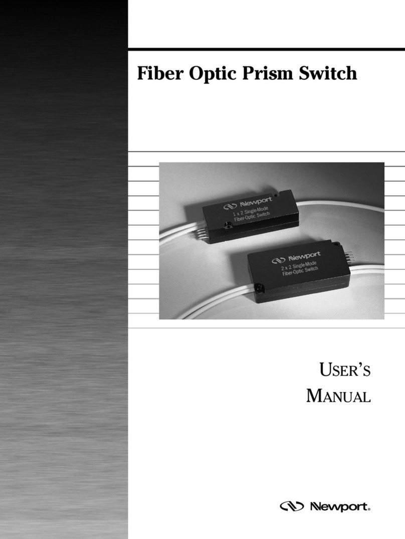
Newport MS-1315TT-12 User manual

MEMS MS1X2 Optical Switch
Operation Manual

2
This Product is ESD sensitive
Please take all necessary precautions
when handling the MEMS switch

3
Contents
1. PRODUCT OVERVIEW.................................................................................................................4
1.1 MEMS 1x2 Optical Switch ..................................................................................................4
2. SWITCH OPERATION...................................................................................................................5
2.1 Pin Assignments.................................................................................................................5
2.2 Electrical Specifications......................................................................................................6
2.3 Environmental Specification ...............................................................................................6
3. MECHANICAL DIMENSIONS.......................................................................................................7
4. TTL INTERFACE...........................................................................................................................8
4.1 Parallel Digital I/O Control ..................................................................................................8
4.2 Parallel Digital I/O Timing ...................................................................................................8
5. HANDLING FIBEROPTIC COMPONENTS AND CABLES..........................................................9
5.1 Handling Fiber Optic Cables...............................................................................................9
5.2 Storing Optical Connectors...............................................................................................10
5.3 Cleaning Optical Connectors............................................................................................10
5.4 Mating Optical Connectors ...............................................................................................10
Tables
Table 1. TTL Interface Pin Assignment....................................................................................................5
Table 2. Electrical Specifications .............................................................................................................6
Table 3. Environmental Specifications.....................................................................................................6
Table 4. MEMS 1x2 Logic Table for TTL Interface..................................................................................8
Table 5. Parallel Digital I/O Timing Parameters.......................................................................................9
Figures
Figure 1. MEMS 1x2 Switch Operation Schematic..................................................................................4
Figure 2. Pin Assignment Schematic.......................................................................................................5
Figure 3. Parallel Digital I/O Timing Diagram..........................................................................................8
Figure 4. Fiber optic component, connectors, and fiber pigtails............................................................10

1. Product Overview
This manual is intended for use with the following part numbers:
MS-1315TT-12
MS-1315TT-12-PC
MS-1315TT-12-APC
1.1 MEMS 1x2 Optical Switch
Newport’s MEMS 1x2 Switch is based on a micro-electro-mechanical system (MEMS) chip. The
MEMS chip consists of an electrically movable mirror with two axes of rotation. Voltages applied to the
MEMS chip cause the mirror to tilt along one or both axes, which changes the coupling of light
between a common fiber and N input/output fibers.
The MEMS 1x2 Switch is a non-latching device. When electrical power is removed, the position of the
switch will automatically move to its default position. The default position of a standard MEMS 1x2
Switch is to block the light moving through the switch. Upon request the default position can be set to
one of the 2 fibers.
An operation schematic for the MEMS 1x2 Switch is presented in Figure 1.
Figure 1. MEMS 1x2 Switch Operation Schematic
Note: The above schematic shows the MEMS switch operating in a 1 to 2 application. The common
fiber is used as the input, and the 2 channels are used as output fibers. The switch is bidirectional,
however, and can be used as either a 1x2 or as an 2x1 switch.
When the switch is operated as an 2 to 1, the 2 channels are the 2 inputs and the common fiber is the
output.

2. Switch Operation
2.1 Pin Assignments
The MEMS 1x2 Switch operates through a 14-pin interface. Pin assignments are listed in the following
table. The relative position of each pin is presented in Figure 2.
The 1xN built-in driver is based on an 8051 Microcontroller with external 16-bit D/A converter (DAC)
and amplifier. This driver will support parallel digital data input with STROBE control.
Figure 2. Pin Assignment Schematic
Table 1. TTL Interface Pin Assignment
Pin
Name
Description
Direction
Note
1
NC
No Connection
2
VCC
Power Supply
IN
3
/STROBE
Falling Edge Active
IN
4
GND
Signal & Power Ground
5
D0
Data 0 Input
IN
6
D1
Data 1 Input
IN
1
7
D2
Data 2 Input
IN
2
8
NC
No Connection
9
NC
No Connection
10
NC
No Connection
11
GND
NC
Case Ground for MS1 Switches
No Connection for MSP Switches
12
NC
No Connection
13
D3
Data 3 Input
IN
3
14
/RESET
Hardware Reset; Logic Low Active
IN
4
1. D1 should be connected to Ground for switches with N < 2. For switches with N > 2, D1 is an active
data bit.
2. D2 should be connected to Ground for switches with N < 4. For switches with N > 4, D2 is an active
data bit.
3. Pin 13 serves as the D3 data input. For 1xN switches with N 8, D3 should be connected to
Ground. For 1xN switches with N > 8, D3 is used as the data input.
4. Logic high for normal switch operation. Logic low performs hardware reset.

2.1.1 VCC (Pin 2)
VCC (pin 2) is the power supply pin to the MEMS 1x2 Switch. The value of the supply voltage can
vary within the specified range without affecting the switch output. If VCC is absent, the switch will
revert to the default position (parking state for standard products). The switch will initialize to the
default state at start-up (i.e. at the time VCC receives voltage).
2.1.2 Reset (Pin 14)
Set the reset pin to logic high to allow for normal switch operation. When the reset pin is set to logic
low the switch will reset, which will revert the switch to its default state and reset the internal MCU. The
default state is defined when the switch is manufactured and if not otherwise specified it will be set to
the parking state, which is optically off. Please refer to the “Reset” plot in the timing diagram of section
4.2 for clarification and timing requirements. Also, please be aware that for MEMS switches with
firmware version 3.4 or earlier, this pin is not utilized and can be left floating.
2.2 Electrical Specifications
Table 2. Electrical Specifications
Parameter
Minimum
Maximum
Damage
Threshold
Unit
Latching Type
Non-latching
-
VCC voltage
4.75
13.2
15
VDC
VCC power consumption (at 12V)
-
170
-
mW
Digital I/O logic high
2.0
5.25
5.8
VDC
Digital I/O logic low
0
0.8
5.8
VDC
2.3 Environmental Specification
Table 3. Environmental Specifications
Parameter
Specification
Unit
Operating Temperature
-5 to 70
oC
Storage Temperature
-40 to 85
oC

3. Mechanical Dimensions
Figure 3. MS1 with Bare Fiber Mechanical Specifications

4. TTL Interface
4.1 Parallel Digital I/O Control
TTL control is only available for switches having up to 16 channels since there are four TTL control
pins (D0, D1, D2, D3).
With TTL control, switches with <16 channels may be set to a parking state (<-50dB Crosstalk on all
channels) by selecting the “N+1” channel. For example, with a 1x4 switch, the parking state is defined
as channel 5 within Table 5 below. For switches with 16 channels, the parking state is not available
with TTL control.
Table 4. MEMS 1x2 Logic Table for TTL Interface
Channel
D3
D2
D1
D0
Channel 1
0
0
0
0
Channel 2
0
0
0
1
Channel 3
0
0
1
0
Channel 4
0
0
1
1
Channel 5
0
1
0
0
Channel 6
0
1
0
1
Channel 7
0
1
1
0
Channel 8
0
1
1
1
Channel 9
1
0
0
0
Channel 10
1
0
0
1
Channel 11
1
0
1
0
Channel 12
1
0
1
1
Channel 13
1
1
0
0
Channel 14
1
1
0
1
Channel 15
1
1
1
0
Channel 16
1
1
1
1
4.2 Parallel Digital I/O Timing
Strobe
D0:D3
Optical
output
Reset
Vcc
Tsw
Tsu
Tstb
Th
PWR_RDY CMD_RDY
MCU_RDYMCU_RST
Strobe
D0:D3
Optical
output
Reset
Vcc
Tsw
Tsu
Tstb
Th
PWR_RDY CMD_RDY
MCU_RDYMCU_RST
Vcc
Tsw
Tsu
Tstb
Th
PWR_RDY CMD_RDY
MCU_RDYMCU_RST
Figure 3. Parallel Digital I/O Timing Diagram

Table 5. Parallel Digital I/O Timing Parameters
Parameter
Description
Min
Max
Units
Tsu
Setup time. The channel address
<D0:D3> and RESET inputs must
remain stable preceding the
falling edge of STROBE
1
-
μs
Th
Hold time. The channel address
<D0:D3> and RESET inputs must
remain stable following the
falling edge of STROBE
10
-
μs
Tstb
STROBE pulse width
1
μs
Tsw
Switching time. During this
period the switch would have no
optical transmission on all
channels.
1x2 –10ms
1x4 / 1x8 –
20ms
1x12 –30ms
ms
PWR_RDY
Power-up ready. No channel
switching possible and
STROBE/TTL control would not
work during this startup time.
-
200
ms
MCU_RST
A falling pulse will revert the
switch to the default state
-
100
μs
MCU_RDY
MCU reset ready begins from the
rising edge of the reset pulse
-
10
ms
CMD_RDY
Command ready. The delay is
required between two strobe
signals
-
15
ms
5. Handling Fiberoptic Components and Cables
Fiber optic components require special handling. Follow these guidelines when handling the cables
and connectors.
5.1 Handling Fiber Optic Cables
To avoid cable damage and to minimize optical loss, follow these guidelines when handling fiber optic
cables.
•Handle the fiber pigtail outputs carefully.
•The minimum bend radius for most optical cables is 35mm. Never bend an optical cable more
sharply than this specification. Optical performance will degrade, and the cable might break.
•Avoid bending the optical cable near a cable strain relief boot. Bending an optical cable near a
strain relief boot is one of the easiest ways to permanently damage the optical fiber.

•Avoid bending the optical cable over a sharp edge.
•Avoid using cable tie wraps to hold optical cable. Tie wraps when tightened can create micro-
bends or break an optical cable. Microbends can cause a dramatic reduction in optical
performance.
•Do not pull on the bare fiber as this can break the fiber inside the component.
•Avoid using soldering irons near optical cables. Accidental damage can easily occur when a
soldering iron is used near an optical cable. In addition, solder splatter can contaminate and
permanently damage optical fiber connectors.
•To assure the most stable, repeatable optical performance after the optical cables have been
connected, immobilize the cables using wide pieces of tape or another form of mechanical
cushion.
5.2 Storing Optical Connectors
All switches that include optical connectors are shipped with dust caps covering those optical
connectors. Optical connectors should always remain covered when the instrument is not in use.
Figure 4. Fiber optic component, connectors, and fiber pigtails
5.3 Cleaning Optical Connectors
Clean any exposed connector using a cleaning kit supplied by the connector manufacturer or high-
grade isopropyl alcohol and a cotton swab. To clean with alcohol and a swab, dab the tip of a cotton
swab in alcohol and then shake off any excess alcohol. The tip should be moist, not dripping wet.
Stroke the swab tip gently across the surface of the connector and around the connector ferrule. Either
allow the connector a minute to dry or blow-dry the connector using compressed air. Be careful when
using compressed air: improper use may deposit a spray residue on the connector.
5.4 Mating Optical Connectors
Follow these instructions when mating optical connectors.
•Clean both connectors prior to mating. Any small particles trapped during the mating process can
permanently damage the connector.

•Smoothly insert the appropriate connector ferrule into the adapter. Do not allow the fiber tip to
contact any surface. If the tip accidentally contacts a surface before mating, stop. Re-clean the
connector and try again.
•Tighten the connector until it is finger tight or to the torque specified by the connector
manufacturer. Do not over-tighten the connector as this can lead to optical loss and connector
damage.
•Check the optical insertion loss. If the loss is unacceptable, remove the connector, re-clean both
ends of the mate, and reconnect them. You may have to repeat this process several times before
a low-loss connection is made.
•After you make the connection, monitor the stability of the optical throughput for a few minutes.
Optical power trending (slowly increasing or decreasing) is caused by the slow evaporation of
alcohol trapped in the connector. Continue to monitor optical power until it stabilizes. If the loss is
unacceptable, re-clean the connectors and start again.
This manual suits for next models
2
Table of contents
Other Newport Switch manuals
Popular Switch manuals by other brands

Hama
Hama 00054406 operating instructions

Cisco
Cisco Nexus 9332D-H2R NX-OS Hardware installation guide
IRT
IRT DDS-1100 Instruction book

Enterasys
Enterasys MicroMMAC-T user guide
Hubitat Elevation
Hubitat Elevation C-7 Registration and setup

Lightwave Communications
Lightwave Communications System Console Switch user manual
