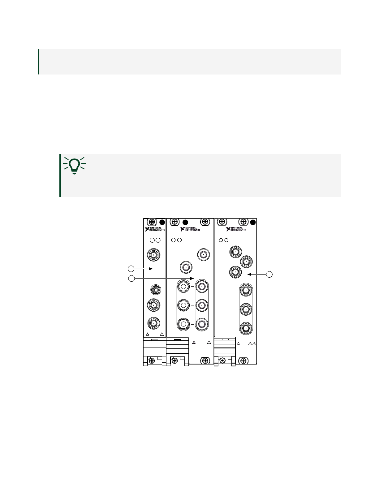
1. Select the master NI 5603 module that is identified as not configured in
the configuration tree.
2. In the Associated Devices section, select the appropriate module from
each system component drop-down listbox.
For the master NI 5665, you must associate the NI 5622 IF digitizer
module and the NI 5653 LO source module.
3. Select the slave NI 5603 module that is identified as not configured in
the configuration tree.
4. In the Associated Devices section, select the appropriate module from
each system component drop-down listbox.
For the slave NI 5665, you must associated the NI 5622 IF digitizer
module and you must select External as the LO source for each slave
device because the LO signals are shared by all NI 5665 devices.
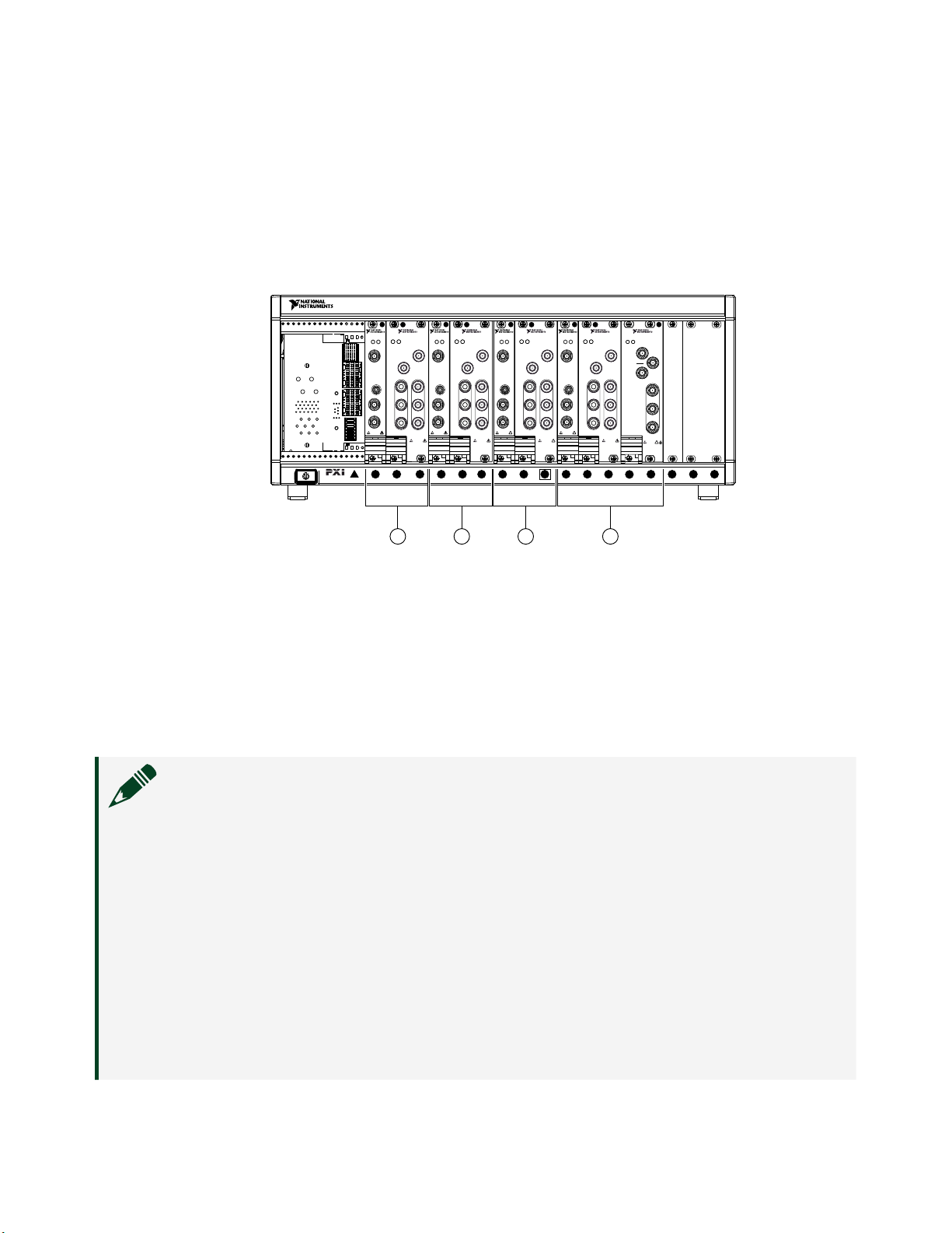
5. Click Save in the MAX toolbar.
Note Module associations may be lost when you move the modules
to dierent chassis slots.
6. Self-test the device modules by selecting the modules in the configuration
tree, and clicking Self-Test in the MAX toolbar. Repeat this step for all
modules in your NI 5665 system.
The MAX self-test performs a basic verification of hardware resources.
Where Do I Go from Here?
Now that you have installed your hardware, interconnected the modules, and
configured the modules in MAX, you can begin programming your hardware using
the NI-RFSA instrument driver.
Visit ni.com/mimo for more information about how to start creating your MIMO
application. This web site provides many useful MIMO articles, videos, and example
programs.
The following documents provide more information that you may need as you
create your MIMO application:
ni.com
10
PXIe-5665 3.6 GHz Getting Started