N10357
-
128 Bit IO Board User's Manual
8
SECTION 3
Operation
The card works by transferring data from the computer bus through a bus interface
chipset
and into a set of latches driving the output drivers. The data transfer is NOT synchronous
across ports, that is, the port data is delivered to the output pins as it is written to the card
addresses.
Similarly, the data on the input port pins moves through a set of optocouplers and buffers
through the bus interface chipset to the computer data bus. Again, the data from the port is
asynchronously available to the computer. Sequential port reads transfers instantaneous data to
the computer, not latched data.
There is a watchdog timer that disables the outputs if not refreshed. It is
always
E
NABLED and must be refreshed
for the outputs to be active. The watchdog operation is covered
in Section 3.3.
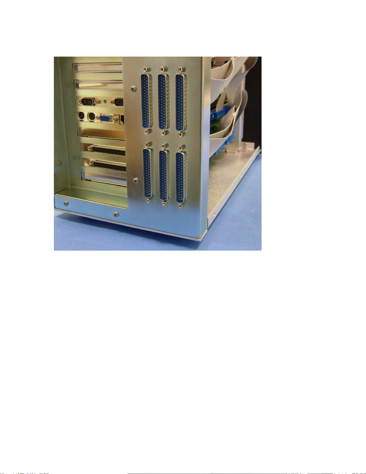
The common for the power provided MUST be the same as the computer common. J2
pins 10, 15, 26, 31, and 36 are common pins. J3 pins 2, 7, 12, 17, 23, 28, and 33 are common
pin
s.
J4 pins 12, 17, 28, 33 are common pins.
The connectors of the card are shown in the next photograph.
3.1
Powering the Input Optocouplers
Pin 1 on J1, J2, J3, and J4 is a power pin that allows power for the optocouplers and/or
the output drivers to be brought onto the card. J2, J3, and J4 each have output drivers attached
to them, and pin 1 on each provides power to a set of output drivers. This configuration allows
drivers on different connectors to run at different output voltages.
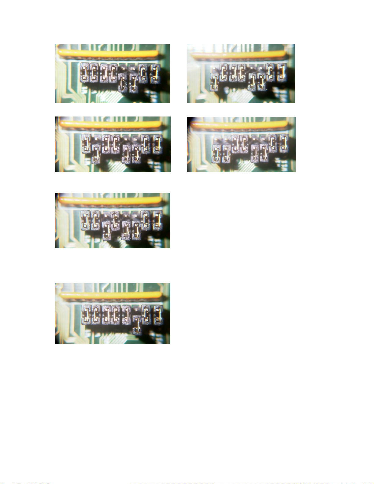
JP1,
JP2, JP3, and JP4 select the power distribution to the input optocouplers. JP2
routes
power for the drivers on connector J2
to all of the input optocouplers
. JP3
routes
power for
the drivers on J3 to the input optocouplers. JP4
routes
power for the drivers on J4 to the input
optocouplers
. Additionally, JP1 may select pin 1 on J1 as the input optocouplers
power source
even though no drivers are attached to J1
.
At least one jumper must be set to use the board inputs, and this is normally a +24VDC
source.
If multiple jumpers are set, the user must NOT have different voltages present on the two
(or more) connectors. For example, if +24VDC is connected to pin 1 of J1, and +12VDC is
connected to pin 1 of J2, setting both JP1 and JP2 will connect the +24VDC and +12VDC power
supplies together, possible damaging the power supplies and the card.